A Proposed Cascode Current Mirror Biasing
Bulk-Driven LV LP OTA
Deepak Goel1 and Jasbir Kaur2
ME Student, Department of E & C Engineering, PEC University of Technology, Chandigarh, India1 Assistant Professor, Department of E & C Engineering, PEC University of Technology, Chandigarh, India2
ABSTRACT: As the biasing circuitry is one of the most important parts of an analog design. The purpose of the bias circuitry is establish an appropriate DC operating point for the transistor. In this paper the design has been proposed of bulk-driven two-stage CMOS amplifier using cascade current mirror biasing method in gpdk 90nm technology. Cadence virtuosoananog environment simulation results confirm the proposed OTA circuit. In fact, a gain (Av) 56.52 dB and phase margin 76.33 deg at lower input voltage (0.4) has been achieved. In addition this new method allowed us
to reduce a slew rate (SR) of 0.5 V/μs at ±0.7V supply voltage. Eventually the average power consumption is reduced
to 13.29μW as compare to existing simple current mirror biasing while driving 1 pF load capacitor.
KEYWORDS: OTA, CMOS, Gain, LP, LV, Cascode current mirror, Bulk-driven MOS, Biasing, output resistance. I. INTRODUCTION
The implementation of high performance signal processing and signal conditioning block is one of the most important task in real-time system designing. Operational amplifiers (Op-amps) are one such among various essential components of any kind of signal processing task ranging from simple amplification of week signals to complex audio and video processing applications in mixed-signal domain.
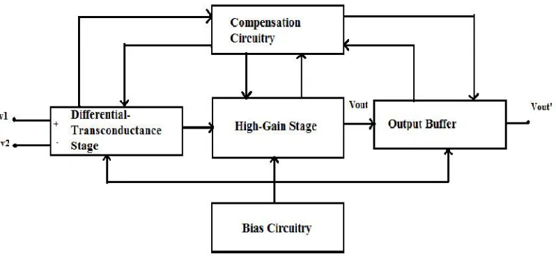
The OTA is an amplifier whose differential input voltage produces an output current. Thus, it is a voltage controlled current source. There is usually an additional input for a current to control the amplifier's transconductance. An OTA is similar to a standard operational amplifier in that it has a high impendence differential input stage and that it may be used with negative feedback as shown with the help of block diagram in fig.1. Portable electronics with low-voltage operation finds big markets. However, the threshold voltage is not reduced proportionally with the supply voltage. Thus, the threshold voltage is becoming a restraint for many analog circuits. Some special techniques are used to overcome the size of the threshold voltage, e.g. floating gate transistors, bulk-driven transistors, continuous-time filters and low threshold transistors. They suffer from several drawbacks or need special fabrication steps, which increases the cost. It is preferred to implement low-voltage circuits using a standard CMOS technology [1].
The objective of the design methodology in this paper is to propose a cascode current mirror biased two stage bulk driven CMOS operational transconductance amplifier. To do this, a simple analysis with some significant parameters (gain, phase margin, power consumption, slew rate etc.) is observed.
II. CURRENT MIRROR IN OP-AMP
One of the most important parts of an analog design is the biasing circuitry. The purpose of the bias circuitry is establish an appropriate DC operating point for the transistor. With the correct DC operating point established a stable and predictable DC drain current ID and a DC drain-source voltage ensures operation in the saturation region for all input signals that may be encountered. This component forms the basis for an operational amplifier whereby various circuits like the deferential pair, gain stage and output stage rely on its flawless stable operation [6].
Fig1. General block diagram of two stage Op-Amp
A. Cascode current mirror:
The basic simple current source with NMOS transistors (M, M’) is shown in fig.2.
Fig. 2: Simple Current Source
Cascode current source has higher output resistance than the simple current mirror. The expression of input and output impedance (Rin, Rout) can be analyzed as follows:
R
=
+
(1)=
. (2)
Where gm is a transconductance and gO is the output conductance of M13, M12. In fact, cascode current source is used
in many designs, including, to increase the current source output resistance by a large factor. Each cascode stage increases the output resistance by a factor of (1+gm.rout) where rout is the output resistance. It also increases the power
dissipation in saturated transistors. For this reason we use a simple cascade current source to assist the system designer in achieving low power consumption [6].
Fig.3: Cascode Current Source
III.BULK DRIVEN OTA USING SIMPLE CURRENT MIRROR BIASING
An important factor concerning analog circuits is that; the threshold voltages of future standard CMOS technologies are not expected to decrease much below what is available today. Though the MOS transistor is a four terminal device, it is most often used as a three terminal device since the bulk terminal is tied either to the source terminal, to VDD or to VSS. Therefore, a large number of possible MOS circuits are overlooked; hence a good solution to overcome the threshold voltage is to use the Bulk-driven principle [7].
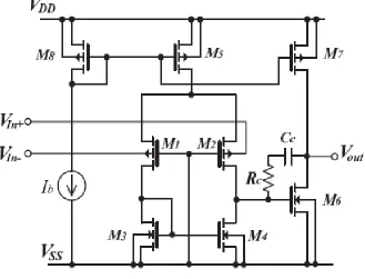
The Driven two stage OTA is shown in Fig.4. It consists of two stages, the first which is combined of the Bulk-driven differential stage with pMOS input devices M1 and M2 and the current mirror M3 and M4 acting as an active load. The second stage is a simple CMOS inverter with M6 as a driver and M7 acting as an active load. Its output is connected to its input, i.e., to the output of the differential stage by means of compensation capacitance Cc and resistance Rc since the compensation capacitance actually acts as a Miller capacitance in that stage. By setting the gate
becomes a depletion type. Input voltage is applied to the bulk-terminal of the transistor to modulate the current flow through the transistor [8] [9].
Fig 4. Two stages Bulk-driven OTA
IV.BULK DRIVEN OTA USING CASCODE CURRENT MIRROR BIASING
This current mirror uses a minimum of five transistors shown in the Fig.5 as comparison to the simple current mirror which uses a minimum of three transistors shown in fig.4.This circuit is a little bit more complex than the simple current mirror with two additional transistors.The main advantage to this design is that it provides stable current. In addition to this we have a higher output resistance compared to the basic current mirror. Thus, due to this advantages cascode current mirror biasing can be a best choice among all types of current mirror biasing.
V. SIMULATIONS AND RESULTS
To analyse the OTA all the transistors must be in saturation region. So after dc analysis we can see the fig.6 that all the transistors are showing their respective specification i.e. id, vgsgm and region. Here the region 2 showing that all the
transistors are in saturation region.
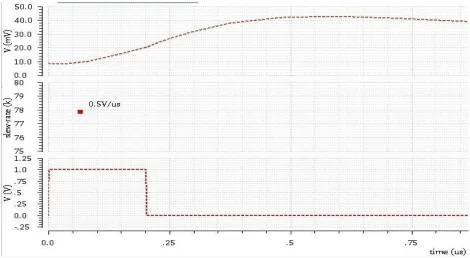
As shown in fig.7, the simulated output frequency response has been presented. Where the bode diagram gives a phase margin 76.33°, a high open loop gain of 57.87 dB. Fig.8 shows the transient behaviour of OTA which shows at which rate output is changing with respect to time under large signal condition. This specification known as the slew rate in op-amp which is measured 0.5V/μsec.
VI.COMPARATIVE ANALYSIS
Fig.5 A Proposed cascode current mirror biased BD-OTA
Fig.7 AC Response of Bulk-driven cascade OTA
Fig.8 Transient response of Bulk-driven cascade OTA
Parameters Bulk-Driven OTA using simple current mirror biasing
A Proposed Bulk-Driven OTA using cascode current mirror biasing
Technology [nm] 90 90
Gain [dB] 53.45 57.87
Average power consumed
[μW]
21.93 13.29
Phase margin [deg] 90.33 76.33
Slew rate [V/μsec] 0.7 0.5
Bulk input voltage [V] 0.4 0.4
Bias current [μA] 10 5
Measurement condition: Vdd= 0.7V, Vss= -0.7V, Cc = CL=1pF, RL= 1MΩ
VII. CONCLUSION
This work presents a novel design method of cascode current mirror biasing two-stage CMOS OTA which has been designed and compared with a simple current mirror biasing bulk driven two-stage CMOS OTA. Behavioral simulation on cadence virtuoso analog environment indicated that phase margin is 76.33° to ensure a good stability, gain of 56.52 dB for ±0.7V without using a gain boosting technique. The applied technique leads to a significant preservation in gain (Av), slew rate (SR), and average low power consumption. The design technique proposed in this paper is that it provides stable current. In addition to this we have a higher output resistance compared to the basic current mirror. Thus, it can be scored high in our choice for current mirrors in comparison to other current mirrors.The mainly use of such type OTA can be in biomedical applications as to design filters.
REFERENCES
1. David Johns and Kenneth W. Martin, "Analog Integrated Circuit Design", John Wiley & Sons, 1997.
2. F.Silveira, D. Flandre and PGA Jespers, “A gm/ID based methodology for the design of CMOS analog circuits and its application to the synthesis of a silicon-on-insulator micropower OTA”, IEEE Journal of solid state circuits, vol.31, No.9, September 1996.
3. M. Ghovanloo and K. Najafi, “A compact large voltage compliance high output impedance programmable current source for implantable microstimulators”, IEEE Tran. Biomed. Eng., vol. 52, pp. 97-105, Jan.2005.
4. Mr. Bhavesh H. Soni, Ms. Rasika N. Dhavse, “Design of Operational Transconductance Amplifier Using 0.35μm Technology”,
International Journal of Wisdom Based Computing, Vol. 1 (2), August 2011.
5. MajidMemarianSorkhabi and SiroosToofan, “Design And Simulation of High performance Operational Transconductance Amplifier”, Canadian Journal on Electrical and Electronics Engineering Vol. 2, No. 7, July 2011.
6. BehzadRazavi, “Design of Analog CMOS Integrated Circuits”, McGRAW-Hill international edition, p.p. 291-335.
7. B. J. Blalock, H. W. Li, P. E. Allen, and S. A. Jackson, “Body-driving as a low-voltage analog design technique for CMOS technology”, IEEE Southwest Symp. on Mixed-Signal Design (SSMSD) 2000, pp. 113-118, February 2000.
8. F. Khateb, “Bulk-driven Op-Amps for low power applications”, Elektrotechnikaainformatika 2003, Nečtiny Castle, 2003, pp. 51 -55.
9. George Raikos, SpyridonVlassis, “0.8 V bulk-driven operational amplifier”, in Analog Integrated Circuits and Signal Processing, 2009.
BIOGRAPHY
Deepak Goel received his B.Tech degree in Electronics & Communication Engineering from Moradabad Institute of Technology, Moradabad, UP, India in 2012. He is pursuing M.Tech degree in Electronics (VLSI Design) from PEC University of Technology, Chandigarh, India since 2014. His research interests include low power techniques, analog electronics, digital electronics and VLSI design.