Scholarship at UWindsor
Scholarship at UWindsor
Electronic Theses and Dissertations Theses, Dissertations, and Major Papers
1-1-1970
A data flow controller and refresh memory for a computer display
A data flow controller and refresh memory for a computer display
system.
system.
David Logan Murray University of Windsor
Follow this and additional works at: https://scholar.uwindsor.ca/etd
Recommended Citation Recommended Citation
Murray, David Logan, "A data flow controller and refresh memory for a computer display system." (1970). Electronic Theses and Dissertations. 6867.
https://scholar.uwindsor.ca/etd/6867
AND REFRESH MEMORY FOR A COMPUTER
DISPLAY SYSTEM
by
DAVID LOGAN MURRAY
A Thesis
Submitted to the Faculty of Graduate Studies through the Department of Electrical Engineering in Partial Fulfillment of the Requirement for the Degree of
Master of Applied Science at the University of Windsor
IN F O R M A T IO N T O U S E R S
T h e quality of this reproduction is d e p e n d e n t upon th e quality of th e copy
subm itted. Broken or indistinct print, colored or poor quality illustrations and
photographs, print bleed-through, substandard m argins, and im proper
a lig n m en t can ad versely affect reproduction.
In th e unlikely e v e n t that th e auth o r did not send a c om plete m anuscript
and th e re a re missing pages, th e s e will be noted. A lso, if unauthorized
copyright m aterial had to be rem o ved , a note will indicate th e deletion.
UMI
U M I M icroform E C 5 2 8 2 2C opyright 2 0 0 8 by P ro Q u e s t LLC.
All rights reserved. T his m icroform edition is protected against
u nauthorized copying under Title 17, United S ta te s C ode.
P ro Q u e s t LLC 7 8 9 E. E ise n h o w e r P arkw ay
This thesis presents the design and implementation of a
digital controller and high speed refresh memory for a cathode ray
tube (CRT) display terminal.
The specific function of this device was the control of and the
£3J pply of data to graphical and alphanumeric display generators that
were also in the development stages. The system for CRT display was
to be used in conjunction with a Digital Equipment Corporation (DEC)
PDP8/S computer.
The slow cycle speed and single stream processing of the PDP8/S
made the development of control and refresh circuitry necessary to free
the computing facilities of the PDP8/S for programmed data processing
necessary for the effective use of CRT display equipment.
The device described in this thesis was constructed and interfaced
to the PDP8/S through the standard input-output (I/C) facilities of the
PDP8/S which "sees" the device as one of its peripherals. Thus the
PDP8/S has been fitted with CRT display facilities over which it exerts
indirect control through the logic presented in this thesis. The PDP8/S
is, therefore, not operating as a dedicated computer but is free to per
form any other program tasks and I/C to its other peripherals while
The author wishes to express his appreciation to
Dr. P. A.V. Thomas who supervised this work and for his helpful
suggestions. Acknowledgement must also go to the National Research
Council of Canada for the financial aid which made this project
ABST RACT iü
ACKNOWLEDGEMENTS iv
TABLE CE CONTENTS v
LIST CE ILLUSTRATIONS . vit
Chapter
I. INTRODUCTION
1.1 General Aspects and Classification of
the Problem 1
1.2 The Problem and Design Criteria 3
II DESIGN PHILOSOPHY
2.1 Preliminary Design Decisions 8
2.2 System Design Concepts 12
(1) Introduction 12
(2) Refresh Addressing, Looping and
Branching by Embedded Instructions 12
(3) Data Channelling 19
(4) Display Pile Word Format 20
(5) Memory Cycle Initiation and Display
Refresh 23
(6) PDP8/S Interaction with DEC and Refresh
(8) System Block Diagram and Summary 44
III SYSTEM LOGIC
3.1 Introduction 47
3.2 Memory Timing and Control 47
3.3 DEC and Decoder Logic 55
(1) Notation and Figures 55
(2) Initiation/Shut Down Logic 55
(3) Memory Cycle Initiation and Priority
Logic 56
(4) H201 Memory Input and Output 61
(5) DEC Processing of Display Files 63
(6) Indicator Light and Single Cycle
Operation 73
IV IMPLEMENTATION AND RESULTS 75
APPENDIX I - KEY TO FIGURE VIII 76
APPENDIX II - LOGIC NOTATION 79
REFERENCES 84
Figure Page
I DAR and DBR Bit Transfer Arrangement 16
II Display Memory Map 18
III Display Refresh Timing Block Diagram 25
IV Typical Display File 26
V . Typical I/O Instruction 38
VI W103 Module Configuration 38
VII PDP8/S lOP Pulse Timing 38
VIII System Block Diagram 45
IX H201 Memory Cycle Timing 48
X Memory Timing Logic 48
XI. Swap Tail Ring Counter 49
XII STRC Timing ' 49
XIII DFC and Decoder Logic - 1 53
XIV DFC and Decoder Logic - 2 54
INTRCDUCTICN
1,1 General Aspects and Classification of the Problem.
The display of visual information may be divided into three
areas; preparation of data into the appropriate digital coding, control
of data flow and rate of flow, and the processing of this data into a
form suitable for display. This thesis deals with a device to control
data flow and rate of flow in a particular CRT display system.
In general, visual information may be separated into two clas
sifications; text and graphical. Text generally consists of alphanu
meric information but may also include any special characters common
ly used. Graphical data consists of information necessary for the
display of drawings, figures, graphs, or any non-standard shapes.
Graphical data may be subdivided into further categories such as
vector (straight line), dot, circle, sector, etc. The classification of
visual display data is subject to interpretation. However, the
importance of data classification to the control of data flow lies in
the fact that different types of information must be processed for CRT
display by different Display Generators. Thus, information must be
oversees the data flow must direct the data into the proper channel and
in the proper sequence. This device or controller may be software,
or hardware in nature or a combination of both.
A second problem involved in the CRT display of visual data
is that of rate of flow. Two types of CRT display are possible; the
firs t employs a memory tube which retains any trace that is applied
to it, and the second uses a conventional CRT which requires a con
stant and rapid retrace or refresh of a trace and depends on the image
retention of the human eye to hold a constant image. The former
approach is the simpler to implement but its use removes the possi
bility of man-machine interaction through the use of a light pen
(Chapter II); the latter method although more costly and difficult to
implement facilitates the use of the light pen and it was the approach
used in the device described in this thesis. Discussion will, therefore,
be limited to the rapid refresh approach.
The refresh rate of information displayed on a CRT depends
upon the phosphors used in the CRT itself but a lower lim it of this
refresh rate can generally be set at thirty frames per second necessary
for a non-flickering image retention with phosphors commonly used.
Thus, visual data not only has to be channelled to the appropriate
generator but also at the correct rate. That is, fast enough to
faster than the generators can process the data for display. The pro
blem is further complicated by the fact that the different generators
will likely process their data at different rates.
The remainder of this thesis deals with a particular data flow
problem and its solution.
12 The Problem and Design Criteria.
Based on research previously carried out in the Electrical G)(2)
Engineering Department of the University of Windsor and on
(3)
research currently in progress interest became aroused in the
construction of a CRT display terminal. After careful consideration
the design problem involved in developing a CRT display system
divided itself into three areas: the design and implementation of an
alphanumeric (A/N) character generator, the design and implementa
tion of a vector and dot generator, and the design and implementation
of a data flow controller and refresh circuit. The latter design area
is dealt with in this thesis.
Both the control of data flow and the refresh of a CRT may be
implemented by software techniques. The only computer available for
(
4)
this project was the DEC PDPB/S. A quick examination of the
feasibility of using the PDPB/S for a software implementation of
control and refresh led to the following minimum cycle time for the
Clear Accumulator 28
Two's Compliment Add 36
1/O Instruction 38
Total 102 ysec
The above program sequence represents the absolute minimum
time required to output a single word of data and in practice the average
output time would be much higher due to program decisions regarding
data channelling and necessary program looping. However, even if
we consider the above 102 ysec as the average cycle time for a single
piece of data and if we take the lower lim it of thirty frames per second
refresh rate the maximum number of data words that may be displayed
on a CRT in one image is:
—6
(1/30 sec)/(102 X 10 sec) = 328
or approximately five of the printed lines on this page if we consider
A/N data only. Thus, if the PDP8/S was to handle the refresh of the
CRT display the amount of data available for display would be seriously
limited. Perhaps an even more restricting factor lies in the fact that
the programmed data processing capabilities of the PDP8/S would be
almost completely tied up with refresh and control of data flow and
would not be available for programmed data manipulation that makes
a CRT display terminal a useful device. It, therefore, became obvious
that some type of a hardware circuit would be necessary to handle the
the processor of the PDP8/S.
After the decision was reached to design and implement a hard
ware control and refresh device it was necessary to decide upon a set
of necessary and desirable operating features. The lis t of operating
features deemed necessary for minimum acceptable operation were
as follows:
(i) This device must have some type of memory capable of storing
a display file and cycling through this display file to supply
data to display generators at a rate as fast as the generators
could process the data for CRT display. This would insure
the display of the maximum amount of data at an acceptable
refresh rate.
(li) This device must have the ability to accept data from the I/O
channel of the PDP8/S for the purpose of building up the contents
of its display file. Thus, the contents of the display file would
be under the control of the PDP8/S while the refresh of this
data would be handled by the external refresh memory.
(iii) Since data of several types (i.e. A/N, dot, vector) was to be
displayed, this device must have the ability to channel data to
the appropriate generator.
The above list of design criteria were necessary to the
usefulness of the system. These additional features are listed below:
(i) The ability of this device to hold in its memory multiple
display files of variable length coupled with the ability to
select one of these for refresh under PDP8/S control
would greatly improve the systems smoothness of operation
while reducing the storage requirements of the memory of
the PDP8/S.
(ii) The ability of this device to accept single or block data changes,
insertions, deletions or additions to any of its display files
whether or not they are currently being refreshed without
interrupting the display would make possible very effective
on-line editing of information.
(iii) In the event that man-machine interaction would be implemented
the potential for this device to retain the position of any piece
of data in the display file upon a light pen interrupt would be
essential for the possible processing of this particular data
word by the PDP8/S .
One further restraint was placed on the design of the control
and refresh circuits. Since the design of the display generators was
to proceed simultaneously with the design of the data flow controller
and refresh circuitry, the exact nature and characteristics of the
pletion of the data flow and refresh logic. Therefore, it was necessary
to design this device to supply data to an undetermined number of
generators that may operate with a wide variety of timing require
DESIGN PHILOSOPHY
2.1 Preliminary Design Decisions.
Before the design could proceed in any detail a decision had
to be made on the type of memory to be used for the storage of the
display file and for the refresh of the CRT. Three types of memories
were readily available on the market for possible use in this applica
tion: magnetic tape, magnetic rotating memories (i.e. disk, drum or
(5)
delay line)and magnetic core memories. Magnetic tape memories
were immediately eliminated due to the excessive rewind time that
would make refresh cycling impractical. The choice, then, had to
be made between a rotating type of memory and a random access core
memory. A consideration that had to be kept in mind during the
choosing of a specific memory was that of electronic compatibility to
the existing equipment. Both the PDP8/S and the A/N generator,
which was already in the construction stage, used the 0 and -3 volt
logic levels of DEC standard negative logic modules. Thus, any
memory used along with the controller circuitry would have to be
compatible with these logic levels or logic level conversion would
have to be built in at any interface.
nature. At firs t glance it appeared that refresh of data could be
easily implemented using a rotating memory. Moreover, rotating
memories tend to be less expensive per bit of storage capacity than
random access core memories. However, since rotating memories
circulate at a fixed rate any device accepting data from a rotating
memory must do so at a rate dictated by the rate of rotation of the
memory. Data may be accessed a word at a time in some rotating
memories but this approach of random addressing leads to greatly
increased access times that would not permit a reasonable refresh
rate. This problem may be alleviated to a certain extent by the
interlacing of data on the rotating memory tracks. At best, however,
the use of a rotating memory requires that the display generators
accept data at some fixed rate which puts heavy restrictions on the
efficient design of these generators. Rotating memories by their
very nature are best suited for block data transfers. Thus, if
effective editing of the display file was to take place a very efficient
system of memory mapping and data allocation would have to be
maintained in the software of the PDP8/S to insure that the refresh
rate would not fall below an acceptable minimum due to excessive
access time caused by excessive memory address branching.
On the other hand, the random access core memory had the
( 5)
ing circuit. This was not a particularly serious handicap, however,
since a rotating memory would have to be equipped with addressing
logic of comparable complexity if it was to be any use at all. The
random access core memory does not suffer the disadvantages of a
fixed cycling frequency and outputs a data word from any specified
location on command. Therefore, if a random access core memory
were used the generators receiving data from it could set their own
pace (as long as the cycle time was not lower than the minimum cycle
time of the memory) and so remove any synchronization problems.
In addition, since this type of memory may access any address in the
same minimum cycle time, extensive looping and branching could be
implemented without careful consideration of memory space alloca
tions and without increasing the average word access time.
It appeared that the random access core memory had operating
characteristics superior to those of rotating memories for this applica
tion. The last consideration was one of cost. The logical choice of a
random access core memory for investigation was the DEC H201
memory stack as it was compatible with all the existing equipment
in both logic levels and word length. This memory has a 12 bit data
word length, 4096 words of storage, and a minimum cycle time of 8
y sec. Decoding logic was also available from DEC. The cost of the
memory plus decoding and driving logic was approximately $3,300.00.
Systems (IDS) series 8000 disk memory and the DEC disk model
DS32. The IDS series 8000 disk has a storage capacity of 5,800
12-bit words with a word transfer rate of 23 ysec per word. This
disk memory uses a preamble and postamble approach^^'^ to data
block addressing, thus, random access of data words is extremely
wasteful in both memory storage space and in access time with this
memory type. The basic cost cf the IDS disk was approximately
$2,700.00 not including timing and addressing logic and logic level
conversion necessary with use of this memory. The DEC disk model
DS32 has a storage capacity of 32,000 12-bit words and a word trans
fer rate of 66 ysec. This disk is equipped for random access of data
words with an average access time of 16.67 ysec. The price quoted
from DEC for the model DS32 was $3,270.00 and again this price
does not include timing and addressing logic.
■ From the design criteria and cost considerations it was obvious
that the DEC H201 random access core memory would provide much
superior operating characteristics at a slight penalty in price and a
more serious penalty in storage capacity. Flowever, since this
memory was primarily for use as a rapid refresh memory and would
not be used for bulk storage, it was decided that the random access
core memory would provide by far the best compromise. Hence, an
H201 memory stack along with its suggested decoding and driving logic
2. 2 System Design Concepts.
2.2.1 Introduction
After the choice of a memory type, it became neces
sary to reach certain design concepts that would make it possible to
satisfy as many of the design criteria as possible. The system con
ceptualization described in the remainder of this chapter demonstra
ted the ability to satisfy all of the design criteria. For the sake of
continuity this description does not follow in the chronological order
that these concepts were reached. Instead, the system concepts are
presented in an order which will make the overall picture clear. The
block diagram and summary at the end of this section will attempt to
tie each of the concepts presented into a unified picture of the system
and to point out how each of the design criteria outlined in Chapter I
is satisfied.
2. 2.2 Refresh Addressing, Looping and Branching by
Imbedded Instructions.
One of the most attractive features of the random
access core memory was its ability to access data words from any
location in its storage without an increase in access time. It was
decided to exploit this ability as much as possible to improve the
flexibility of the system. Editing of a display file (i.e. changes,
deletions, or insertions) can most easily be achieved by introducing
following display file may be considered typical:
Memory Location Contents
X X + I X + 2 X + 3 X + 4 X + 5
X + 20
DATA A DATA B DATA C DATA D DATA E DATA F
END OF FILE
If it becomes desirable to insert a block of data (of any length)
between DATA C and DATA D , the following modified display file
employing "branch instructions" embedded in it would achieve this
very nicely.
DATA A DATA B DATA C
BRANCH TO X + 21 DATA E
DATA F X
X +1 X + 2
---X + 3 X + 4 X + 5
X + 20
—► X + 21
X + 22 X + 23 X + 24
END OF FILE DATA D
DATA M DATA N
BRANCH TO X + 4
"Thus, DATA M and DATA N have been inserted into the display file
with a minimum of display file rewriting and with the addition of only
two non-data memory cycles. It becomes obvious that a circulating
begin-ning of file instruction" as the last word in the data file. In this way
the display file will circulate to provide a. refresh for the CRT.
It was evident that an addressing system should be developed
that would increment by one the memory address for each word of
"data" that was read out and would modify this address to any memory
location on command of an imbedded branch or jump instruction. In
practice a 12-bit address is required to access all of the 4096 memory
locations in the H201 memory stack. Since the basic word length of
this memory is ori y twelve bits, more than one instruction word
would be necessary if this instruction was to be recognizable
as an instruction, and capable of modifying a 12-bit address. The
decision was made to divide the memory into a "page" type of system
and use two types of jump instructions; direct jumps and indirect
jumps. For direct jumps or one word jumps, the memory was
divided into 16 pages each of 256 memory locations. The direct jump
instruction modifies the last eight bits of the memory address while
leaving the firs t four bits as they were so that any of the 256 memory
locations may be addressed on the current page which is defined by
the firs t four bits of the memory address. Thus, the firs t four bits
of the direct jump instruction are used for instruction identification,
while the last eight are used to modify the memory address. One bit
of the firs t four in the direct jump instruction word was set aside for
memory address to address any location on the current page or the
same location relative to page "0" (i.e. firs t four bits of memory
address are 0000). Thus, the direct jump instruction provides a one
Vi/ord branch instruction that can modify the memory address to access
any of the 256 memory locations on the current page or any of the
memory locations from 0 to 256 (i.e. page 'O’ ). The indirect jump
instruction allows an absolute branch to any location in memory.
This function requires two consecutive words in memory. The firs t
word is recognized as an indirect jump instruction and initiates a
read of the next consecutive word in memory the twelve bits of which
are used as the new memory address. Thus, a full 12-bit address
has been selected for the next memory read.
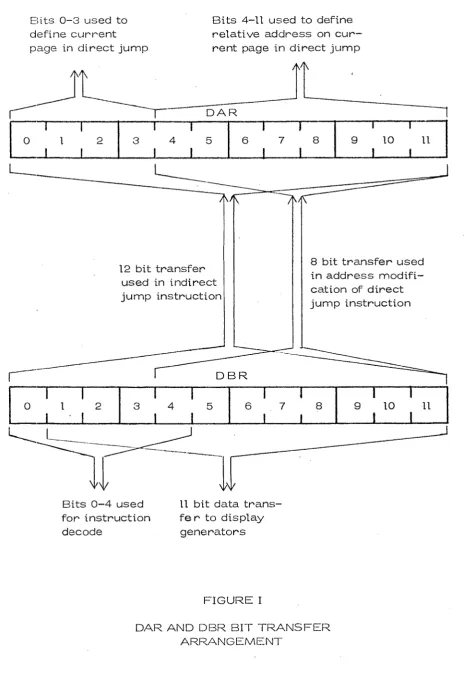
The above addressing system requires the use of two 12-bit
registers; a display address register (DAR) which must have the
ability to act as a ones counter and the ability to be modified for
branching, and a display buffer register (DBR) which receives data
from the memory outputs and acts as a decoding register for embed
ded instructions as well as a buffer register for data words destined
for display generators and the contents of which may be used to modify
the DAR. Figure I gives a graphical representation of some of the
functions of the DAR and DBR.
The display file addressing system described above makes
Eüts 0-3 used to define current page in direct jump
Bits 4-11 used to define relative address on cui— rent page in direct jump
DAR
10
8 bit transfer used in address modifi cation of direct jump instruction 12 bit transfer
used in indirect jump instruction
DBR
10
Bits 0-4 used for instruction decode
11 bit data trans fe r to display
generators
FIGURE I
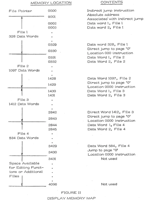
the selection of any of these display files under PDP8/S control. An
example will best demonstrate this ability. Shown in Figure II is a
typical memory map. Let us assume that four separate display files
are stored in the refresh memory. To select a display file the PDP8/S
need only deposit a pointer address in location 0001. That is, the ad
dress 002 deposited in location 0001 will select file number 1, address
0331 deposited in location 0001 will select file number 2, etc. This
depositing of the pointer address need only be done once and the
refresh memory will remain in the proper loop until another selection
is made. Memory locations 3431 to 4096 are still available for addit
ional display files or as space is available for additions or insertions
to any of the display files as described earlier in this section.
To sum up the concept of display file refresh addressing, it is
important to remember that: a data word is recognized by decoder
logic which initiates controller action to increment the DAR by one
memory location, a branch instruction is recognized by decoder logic
which initiates controller action to modify the last eight bits of the
DAR to access a location relative to the current page or page ’O' in
the case of a direct jump or changes the contents of the DAR comple—
tly to access an absolute location in the case of an indirect jump.
Conceptual details of memory cycle timing and of PDP8/S access to
MEMORY LOCATION
F'ile Pointer
File l 328 Data Words
File 2 1097 Data Words
File 3 1412 Data Words
File 4 584 Data Words
0000 0001 0002 0003 0329 0330 0331 0332 1428 1429 1430 1431 2842 2843 2844 2845 3429 3430 3431 Space Available
for Editing Funct ions or Additional Files
CONTENTS
Indirect jump instruction Absolute address
Associated'with indirect jump Data word I, File I
Data word 2, File I
Data word 328, File I Direct jump to page 'O' Location 000 instruction Data Word I, File 2 Data Word 2, File 2
Data Word 1097, File 2 Direct jump to page 'O' Location 0000 instruction Data Word I, File 3
Data Word 2, File 3
Direct Word 1412, File 3 Direct jump to page 'O' Location 0000 instruction Data Word I, File 4
Data Word 2, File 4
Data Word 584, File 4 Jump to page 'O'
Location 0000 instruction Not used
4096 Not used
FIGURE II
2.2.3 Data Channelling.
It was pointed out in Chapter I that a basic function
of the data flow controller and refresh memory was to channel data to
the appropriate display generators. This function could be implemented
in two possible ways. The firs t approach considered was to set aside
a number of bits in the data word itself that could be used to make a
piece of data recognizable to decoder logic as destined for a particular
display generator. For the three display generators already under
development this would require the use of two bits of the data word
for the necessary decoding. If more display generators were to be
added at a later date, additional data word bits would have to be
reserved. Since any word put out from the memory also had to be
recognized as data or instruction (see section 2.2.2.) which requires
the use of one bit, the total number of bits of a data word that could
not be used to pass display information to a display generator would
be a minimum of three or 25% of the available information bearing
space. The second approach was to prefix any block of data (of any
length) with an instruction embedded in the display file which would
indicate to the controller logic that all data immediately following
and up to the reading of a new data channelling instruction word was
to be channelled to the display generator indicated by the prefixing
instruction word. Since data destined for a particular display
in the display file, and since it was undesirable to further shorten the
length of the data word, the second method of data channelling was
adopted. Although this method of data channelling increases the number
of non-data words in a display file it more than compensates with an
increased information carrying capability of data words.
2.2.4 Display File Word Format.
Sections 2.2.2 and 2.2.3 outlined the use of three
types of words that may appear in a display file; the data word, the
jump instruction, and the data channelling instruction. The following
word formats and instruction codes were chosen for programming
convenience.
Data word format is shown below:
0 I 2 3 4 5 6 7 8 9 10 11
0 1 X
_L_. .L.
X X ^ X
L__ J...
X ‘
1
X * X
1
X *
1
X ^
1 X
'O' used to identify this word as a data word rather than an instruction
Bits I-II contain
The following formats are those of jump instructions;
DIRECT JUMP
0 1 2
3
4
5
6 7 8 9 10 111
i
r ” T " ■
1
1
--- 1“
r
1 1 0 X X
X
X
X
X
X
X
____l__
1
1
1
1
1
1 -
1
*1' used to identify this as an
instruction word
Relative address for DAR modification
'1' indicates a jump instruction rather than data
channelling instruction
Bit 3 in ’O' state for direct jump to page
in ’1’ state for direct jump to current pages
’O' indicates direct jump rather than
indirect jump
INDIRECT JUMP
0 1 2 3 4 5 6 7 8 9 10 11
1 1 t 1 T' ' 1 ...1 ..."1.... ...
1 1 1
____L _ . 1_____ - I ___ 1 ... ...L____ J______ 1 1
’ 1’ indicates
instruction rather than data
'1' indicates jump instruction rather than data channelling
instruction
'1' indicates indirect jump rather than direct jump
The format below is that of data channelling instructions
0 8 10 11
--- i... " T — ...1... T ... - ...V....“ T 1
...1---I 0 X X X Y Y Y Y Y Y Y
L - _ i . ... . . ._L_...„ L „ ... J . ___ J___ 1 1
-*1' indicates instruction word
'O' indicates data channelling instruction rather than jumip instruction
7 bits available for transfer of additional control informa.tion to display generators
2.2.5 Memory Cycle Initiation and Display Refresh
Timing.
As was pointed out in Chapter I, one of the problems
involved in the design of a CRT refresh system was that of feeding
data to display generators that operate with a variety of timing
requirements. It was also pointed out in section 2.1 that the use of
a. random access core memory could overcome this difficulty by
allowing each display generator to operate at its own speed. This
section outlines the concepts of the system used to implement display
timing.
The outstanding advantage of using a random access
core memory in any situation where timing may become complex is
its ability to perform a memory cycle only on command from some
esxternal source. In this case the device which initiates a memory
cycle is the data flow controller (DEC). The data flow controller is
cin arrangement of logic and flags that decides which memory location
to access, when to access the memory, and what to do with the
memory word when it arrives. The logic and detailed operation of
the data flow controller are covered in Chapter III. In this section
the data flow controller will be considered as a logic block with certain
inputs and outputs. The interaction between the data flow controller
and the PDP8/S are described in section 2.2.6 but for now it need
refresh memory cycle and from that initial start the DFC governs all
refresh memory cycles.
To achieve display refresh timing one signal line from each
display generator was required by the DFC. The state of this signal
line indicates to the DFC whether that display generator is currently
in generation or sitting idle and ready to accept data. In return, the
DFC supplies a signal line to each display generator which is used
to instruct the generator to read data from the DBR and begin genera
tion.
Once again, the best approach to describing refresh timing is
through the use of an example. Refer to Figure III which is a block
diagram of the refresh timing arrangement and to Figure IV which is
a small but very typical display file. First, assume that the PDP8/S
has initiated the very firs t memory cycle which is a read from location
OOOOq .into the DBR, the value of the DAR and DBR being initially
OOOOg. As the contents of memory location OOOOg arrives at the
DBR, the firs t five bit positions are decoded and this word is recog
nized as an indirect jump instruction. The DFC is signalled the
presence of an indirect jump instruction. The DFC immediately
signals the DAR count logic to increment the DAR by one and then it
initiates another memory read cycle. Due to the actual internal
timing of the H201 memory stack (see section 3. 2) the decoding,
ü
Z
w
D ü
Ll
h I (/)
UJ
E ü
<
LL Û ÜJ
H Z
> o
J
CÛ
5
û_ m5
o; I
D
MEMORY LOCATION CONTENTS DESCRIPTION
- ^ 0 0 0 0
0001
8
8
-0600
06013 0 6 0 2 8
0 6 0 3 8
06048 '0605g 0606g 06078 06108 06118 0700g 07018 0702g 111000000000 000110000000 100100000000 010000110001 000101000100 000000111010 110111000000 010000000000
1 0 0 0 0 0 0 0 0 0 0 0 011010111110 000111101001 110000000000 011101000001 000001001000 110110000101 Indirect Jump Address 600 8 A/N Mode Instruction A/N Data A/N Data A/N Data Direct Jump to Location 700 A/N Data Vector Mode Vector Data Vector Data
Direct Jump to Location OOOOg
'8
A/N Data A/N Data Direct Jump to Location 0605
8
FIGURE IV
is all complete before the completion of the first 8 y sec memory cycle.
Thus the second memory cycle begins immiediately after the firs t with
no unnecessary time loss. As the contents of memory location 0001 g
arrives in the DBR, the DFC "remembers" that this word is a new
address to be used for modification of the DAR and so inhibits any
decoding of this word which may have any bit configuration and thus
cause an erroneous decoding. The DFC then signals the indirect
jump logic to transfer the contents of the DBR to the DAR so that the
DAR now contains the address 0600 . The DFC then initiates a new 8
memory cycle which again follows the preceding one with no loss of
time. As the contents of location 0600^ arrives in the DBR, the word
is decoded as an A/N data channelling instruction or an A/N "mode"
instruction. The DFC then sets a flag to ensure that all subsequent
data words will be channelled to the A/N display generator. The
DAR is then incremented and another memory cycle initiated again
with no unnecessary time loss. The contents of location 0601g arrive
in the DBR and are decoded as a data word. The DFC immediately
senses the A/N generator status line which at this time indicates that
the A/N generator is idle and ready to accept data and a command is
immediately issued to the A/N generator to read the data word. The
DAR is incremented and another memory cycle is immediately
initiated, again no time is lost between memory cycles. The contents
senses the A/N generator status and finds that the generator is still
busy with the last piece of data. The DFC then increments the DAR
but does not initiate a new memory cycle. Instead, the DFC continu
ously senses the A/N generator status and holds the data in the DBR«
As soon as the A/N generator status indicates to the DFC that the
A/N generator is finished, a command is issued to the A/N generator
to read the data already waiting in the DBR. A new memory cycle is
then initiated. Location 603g is read and also contains data and the
last cycle is repeated. Location 0604g contains a direct jump instruc
tion which is decoded upon arrival in the DBR and the DFC is signal
led. The DFC immediately signals the direct jump logic to modify
the last eight bits of the DAR so that the DAR now holds the address
0700g and a new memory cycle is initiated which follows immediately
upon the last one. Location 0700q is thus immediately read and deco
ded as data. The DFC senses the A/N generator status line and finds
that the A/N generator is still busy with the data that was read from
location 0 6 0 3 g . The DFC then increments the DAR and waits for the
A/N generator to finish. (From preliminary research on the display
g e n e r a t o r s i t was estimated that the A/N generator would have the
lowest cycle time of the three generators and that this cycle time
v/ould have a minimum in the neighbourhood of 20 ysec. Thus, the
refresh memory could perform two eight ysec memory cycles before
be executed and a new piece of data to be available in the DBR by the
time the A/N generator is ready for more data). Immediately follow
ing the indication from the A/N generator status line that the A/N
generator is ready to accept more data the DFC issues a command to
the A/N generator to read the data from location 0700g already waiting
in the DBR. The remainder of the display file shown in Figure IV is
processed by the DFC in the same manner as described above.
If the last piece of information in the display file (location
610g) had been destined for the A / N generator, there would be a slight
delay before the firs t piece of data in the display would be directed
to the appropriate generator on the second pass (next refresh) due
to the fact that four instruction memory cycles (locations 0611g, OOOOg,
0001g , 0600g) are necessary between the firs t data cycle and the last.
If we consider the A/N generation time as 20 ysec then the delay would
be approximately 12 ysec (that is 32 ysec the time required for four
memory cycles minus 20 ysec A/N generation time). However, in the
example of Figure IV the last data word is vector mode data and as the
vector generator would likely take considerably longer to process a
word of data, there would not likely be any delay in the data flow to
display generators.
The most notable features of the refresh timing scheme
described above are:
generator must sit idle while waiting for the refresh memory
to deliver data. This means that any display generator with
a minimum cycle time greater than eight usee will be supplied
data as fast as it can process that data for CRT display with very
few exceptions.
(ii) Each display generator sets its own pace so there are no
restrictions placed on the design of the timing of any display
generator. Even if the display generator cycle time is shorter
than that of the memory it will be serviced at a lower than
maximum rate but with no timing difficulties.
2.2.6 PDP8/S Interaction with DFC and Refresh Memory Logic.
Up to this point very little has been said about the communica
tion between the PDP8/S and the CRT display equipment. This section
deals with the mechanics of the PDP8/S control over the CRT display
facilities.
The PDP8/S controls the CRT display system in two ways.
The firs t type of control is its ability to start up and shut down the
operation of the system. Starting up requires an initialization of all
display flags and display registers (the flip-flops of which may come
on in random states at power up) and initiation of the firs t display
refresh memory cycle (that is a read from location 0000^ into the
DBR) as described in the previous section. Shutting down is achieved
registers and flags. Thus, shutting down is, in fact, realized by
reinitialization. The second type of PDP8/S control of the CRT dis
play is by controlling the contents of the refresh memory both by
vv/riting in the original display files prior to the initiation of CRT dis
play operations and by modification additions, insertions, and dele
tions of material in the refresh memory during the time the CRT
display system is actually in operation. This includes the type of
data file selection described in section 2.2.1. As was outlined in the
design criteria, it would be desirable if the second mode of control
could be achieved without disturbing the running of the CRT display
refresh (that is, without temporarily shutting down the refresh memory
to make necessary changes).
Before going into more detail about the PDP8/S access to the
display refresh memory it is worthwhile to go into a brief description
of PDP8/S I/O facilities although for a more thorough and comprehen
sive coverage the reader should refer to the Digital Equipment Corpo
ration publication 'Small Computer Handbook'. The PDP8/S is
equipped with a bus type I/O facility which includes input to and outputs
from its accumulator register, peripheral device selection lines, a
program interrupt line, and an I/O skip line. Peripheral device selec
tion is achieved by external decoding of six device selection lines, the
state of which are set by the I/O instruction being executed by the
three sequential TOP pulses also determined by the I/O instruction
(discussed later in this section). All data communications between
the PDP8/S and the CRT display equipment is in the form of 12-bit
words transferred from and received by its accumulator (AC). A
signal on the Program Interrupt (PI) will cause the PDP8/S to branch
to some predefined subroutine. The I/O skip line is used to inform
the PDP8/S a peripheral device is ready to accept data or instructions
or whether a peripheral has performed an assigned task. The PDP8/S
remains in an I/O loop included in its program sequence for the purpose
of waiting on peripherals until the I/O skip line (IOS) signals it to
branch out of the waiting loop and continue processing.
If the PDP8/S was to have access to the refresh memory it was
necessary that it be provided with access to two registers similar to
tne DAR and DBR. One register must hold the address of the location
that is to be accessed and the other to hold the data to be written into
the memory or receive the data read from the memory. It was con
ceivable that the DAR and DBR themselves could serve this purpose
and so serve a double role. However, this would require that refresh
be halted and the information held in these registers be destroyed each
time the PDP8/S accessed the memory. This would necessitate a
reinitialization and restart for each PDP8/S interrupt of refresh.
Instead, it was decided to provide two registers designated Memory
two registers would be connected to the I/O bus of the PDP8/S and
each would be equipped to accept data from the PDP8/S AC and the
lOB would be equipped to transfer data to the PDP8/S to facilitate
PDP8/S reading of the memory as well as writing into the memory.
Thus, the PDP8/S under program control could output a 12-bit
address to the MAR and a 12-bit display file word to the lOB and then
issue a command to write the word held in the lOB into the memory
location specified in the MAR. Similarly the contents of a refresh
memory location specified in the MAR could be read into the lOB and
then transferred into the PDP8/S AC. During periods when the CRT
display would not be in operation, these transfers would be no pro
blem as the refresh memory could service the PDP8/S exclusively.
However, for refresh memory updates during refresh operation,
timing of PDP8/S memory access cycles presented a problem.
Obviously, since the refresh memory could service only one at a
time, some type of timing system had to be developed that would
allow the CRT display circuits and the PDP8/S I/O to share access
to the refresh memory. As dictated by the design criteria it was
desirable to disturb or delay the CRT refresh functions as little as
possible during such memory access sharing so as to ensure that a
maximum possible amount of display data could be refreshed with a
flicker free refresh rate. This job of refresh memory access co
advantages inherent in the use of a random access core memory made
possible a solution to the problem of dual access timing with minimum
interference to the refresh function. Since the H201 memory stack
has a relatively short cycle time of 8 ysec and since the shortest
display generator cycle time was to be of the order of 20 ysec (actually
this time turned out to be 18.5 ysec), it was apparent that during
refresh of strings of data there would be periods of time in which the
refresh memory would sit idle while the DFC waited for display
generation to finish (refer to the example in the previous section).
These idle periods would be more than long enough for the H201
memory to perform a memory cycle in service of the PDP8/S.
Thus, the DFC could initiate the "stealing" of a cycle from the regular
refresh duties of the refresh memory to accomplish a PDP8/S I/O
memory cycle. These stolen cycles would not effect the regular
refresh timing of the display generators nor would they destroy the
bit configurations currently residing in the DAR and DBR. In addition,
since the minimum time required for the PDP8/S to perform an I/O
program loop or sequence is 102 ysec (as pointed out in Chapter I),
it would be, in almost all cases, very probable that the DFC would
be able to "find" an opportunity to steal a cycle before the PDP8/S
could be ready to request another memory access cycle. Thus, the
PDP8/S would not be materially delayed in processing I/O to the
To implement such a system of dual memory access, the PDP8/S
would have to make its request for a memory access cycle to the DFC
which would hold the request until it found an opportunity to initiate
the cycle and then notify the PDP8/S through the I/O ship line that
the requested cycle had been completed. It should be noted here that
('4')
the PDP8/S would remain in an I/O skip loop^ incorporated in the
program under execution by the PDP8/S until the lOS caused the
DP 8/S to branch out of the loop, but since the DFC would likely
perform the I/O task before the PDP8/S could make another request,
this I/O skip loop may be left out of PDP8/S programs at the discre
tion of the programmer.
The possibility that at some future date a display generator
v/ould be developed with a cycle time less than eight ysec presented
the problem that the DFC would not be able to find sufficient oppor
tunities to cycle steal on behalf of the PDP8/S and so substantially
slow down PDP8/S I/O functions to the CRT display system. It was
therefore decided to implement a "computer override" option that
v\/ould be selected under program control of the PDP8/S and would
cillow the PDP8/S to take priority over the display refresh for display
memory access.
Since a memory may be accessed by only one set of registers
at a time, the above dual access system necessitates that the MAR-IOB
allow them to be switched into or out of access to the memory address
decode, the memory inhibit, and memory output lines of the H201
memory stack. This selection of registers for memory access would
be under DFC control.
The dual access system implies a set of priorities associated
with memory access. Before detailed design of the DFC could start,
this priority system had to be laid down more explicitly. The highest
priority had to be a memory cycle already in execution as it would be
disasterous to initiate a new memory cycle while the memory was
already in mid-cycle. The following list represents the memory
access priority scheme in descending order of priority.
(1) A memory cycle already in execution.
(2) A PDP8/S memory cycle requested while computer override
option is in force.
(3) A display refresh memory cycle.
(4) A PDP8/S memory cycle requested while computer override
option is not in force.
Due to the fact that data transfers between the refresh memory
and the PDP8/S would often take the form of blocks written into
sequential locations in the refresh memory, it was felt that an auto
matic increment facility incorporated into the MAR would provide
more rapid data transfer and reduce program steps. This "auto
register and by having the DFC initiate a one’ s count in the MAR every
time a read or write cycle was requested by the PDP8/S and success
fully completed. This would be an option selected under program
control. Thus, a starting address could be placed into the MAR from
the PDP8/S I/O bus and the auto index option then enabled by a single
I/O command (the option would have to be disabled during the transfer
of a 12-bit address from the PDP8/S due to the logic of a counter
register, see Appendix II) and all subsequent memory cycles would
access memory locations in sequence from the starting address until
the option is disabled by I/O command.
Before a list of the I/O commands developed for the PDP8/S
interaction with the CRT display system is given, a brief discussion
of the PDP8/S I/O command format and operation will be useful.
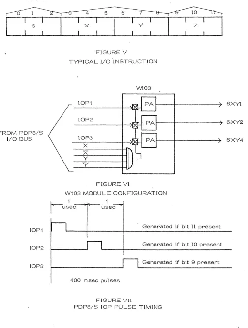
A typical PDP8/S I/O command word has the format shown in
Figure V. Bits 0-2 make up the operation code and are decoded in the
PDP8/S to initiate an I/O instruction sequence. Bits 3-8 make up the
device selection code. Each peripheral device must have in its circui
try at least one W103 DEO standard device selector module(4) (DS)
which is comprised of a 12-input and gate (in actuality this gate is a
NAND gate but fpr the sake of continuity it may be considered as an
AND gate) the output of which enables, through DOD gates (see
AppendixII) three pulse amplifiers (PA) as shown in Figure VI. Bits
CODE SELECTION CODE
... r... "T...
“ 1---
1... ... i
1 1I...
-6 X Y Z
J
____ l.._...
. ...
1. ...
1... ...
1...
1...
1 , 1...
FIGURE V
TYPICAL I/O INSTRUCTION
W103
10P1 PA
IOP2
PA
FROM PDF 8/S
I/O BUS IOP3 PA ^ 6XY4
IOP1
IOP2
IOP3
FIGURE VI
W103 MODULE CONFIGURATION
usee usee
Generated if bit 11 present
Generated if bit 10 present
Generated if bit 9 present
400 nsee pulses
FIGURE VII
applied to the inputs of all DS AND gates. Each DS AND gate is
arranged so that it will "turn on" only with a specified 6-bit code
from bits 3-8. Thus for each I/O command only one DS is enabled.
Bits 9-11 control the generation of the lOP pulses. These pulses are
generated in the I/O logic of the PDP8/S and are available on the I/O
bus if they are selected in the I/O instruction word. Figure VII gives
the timing of the three pulses and indicates that an lOP pulse will be
generated only if the corresponding bit is specified in the instruction
word. Thus, the I/O instruction of the PDP8/S serves the purpose
of applying any combination of three possible pulses to a specific
device among its peripherals. These pulses may be used for trigger
ing data transfers or any variety of control functions.
The following list gives the commands developed for the PDP8/S
interaction with the CRT display equipment and the associated codes.
It should be noted that the firs t section of the list gives the basic
commands (that is; the commands in which only one lOP pulse is
called for so that each of these commands initiates only one function),
the second part of the list gives commands that are combinations of
two or three of the commands in the firs t section of the list (that is;
commands where more than one lOP pulse is specified so that two or
three of the functions of the basic commands are performed by one
instruction word). DS codes were selected to facilitate the combining
Part I
I / O
Instruction Description and Comments
Code
1 6721...Clear lOB
2 6724... Write from lOB into Mem. Log.
Specified in MAR.
3 6722... Load lOB from PDP8/S AC.
4 6734 . . . Read from Refresh Mem. Location
Specified in MAR into lOB
5 6751...Skip if Requested Operation not
Complete.
6 6754...Transfer Contents of lOB into PDP8/S
,AC.
7 6731...Clear MAR
8 6732...Load MAR from PDP8/S AC.
9 6741...MAR Auto Index Enable On.
10 6742... .MAR Auto Index Enable Off.
11 6711... Initialize Display or Shut Down.
12 6712... Computer Override Option On.
13 6714... Computer Override Option Off.
14 6701... Initiate First Display Refresh Memory
P art 11
15 6723...Clear and Load lOB from PDP8/S AC.
Combination of 1 and 2.
16 6725...Clear Memory Location Specified in
MAR. Combination of 1 and 3.
17 6727...Load Memory Location Specified in
I/O
Instruction Description and Comments
Code
18 6733 Clear and Load MAR from PDP8/S
AC. Combination of 7, 8.
19 6737 Read From Memory Location
Specified in PDP8/S into lOB.
A total of six DS modules were used in the actual implementa
tion of the DFC and refresh memory logic. This provides the possi
bility of using eighteen basic commands and as only fourteen were
used, four commands were left for the possible implementation of
future logic such as the light pen system described in the next
section.
2.2.7 Possiblities for Future Implementation of s. Light Pen.
It was pointed out in Chapter I that one of the design criteria
for the DFC and CRT refresh memory was the potential for addition,
at some future date, of a light pen for a higher level of man-machine
interaction. As a light pen implementation.was not part of the
original design problem, no detailed logic designs were attempted.
However, the following conceptualization of such a system will serve
to demonstrate that the system of data flow control and CRT refresh
conceptualized in the preceding sections of this chapter does have the
potential for light pen implementation and so successfully fulfills that
particular design criterion.
device (a light sensitive transistor for instance) mounted in a conven
ient fixture for holding, generally, in the same manner as a ball
point pen. The end of the light pen holding the light sensitive device
is applied directly to the face of the CRT screen. When the CRT beam
travels across the screen and excites phosphors directly under the
light sensitive head of the light pen, a pulse is produced by the light
sensitive device and its associated circuitry. This pulse is used to
initiate some type of computer or controller action. In this case, the
light pen would be placed on a CRT screen area where one of the
display generators was producing a CRT trace. When the beam
causes this area to produce a "burst" of light during the cycling
refresh of the display, it would be desirable to use the resulting
pulse to initiate action to secure and hold the refresh memory
address of the data word that was being processed to produce that
particular trace. This data word address could then be transferred
to the PDP8/S by a program sequence entered when the PDP8/S
received a PI, also initiated by the light pen pulse. The PDP8/S
could then process this data word address for editing, software option
Eielection (menus) or any number of other software applications.
The functions described above could be implemented by the
introduction of a new 12-bit register, possibly designated Data
Address Tracking Register (DATR). This register would hold the
any time when a command is issued from the DFC to a display
generator to read data and begin generation, a simultaneous command
would be issued to the DATR to copy from the DAR the 12—bit address
currently held by the DAR. The DAR itself could not double as the
DATR since, as was previously described, the DFC may execute
several instruction cycles while a data word is being processed by a
display generator, the DAR may no longer hold the address of the
data currently in generation when a light pen pulse is received by
the DFC. In actuality, since the DAR is incremented before a
command is issued by the DFC to the display generators, the address
in the DATR would always be one location ahead of the address of the
data in generation. This, however, could easily be taken into account
by software associated with the light pen operation. With the DATR
operating as described above, when a light pen pulse arrives at the
DFC logic, the DFC would immediately inhibit the transfer of address
from the DAR to the DATR, thus "freezing" the desired address in the
DATR. Simultaneously, the DFC would initiate a PI to the PDP8/S
causing it to jump to a predefined subroutine that would transfer the
contents of the DATR, the outputs of which are connected to the I/O
bus inputs to the PDP8/S AC, into the AC. The PDP8/S could then
process this address according to its software. After processing, the
PDP8/S would have to issue an I/O command to the DFC to discontinue
ready for more light pen interrupts.
The light pen system described above is purely hypothetical
and was not implemented. Therefore, it will be left out of the block ,
diagram and summary included in the next section.
2.2.8 System Block Diagram and Summary
Figure VIII gives a block diagram of the overall system.
Appendix I gives the key to Figure VIII. In the next chapter, where
applicable, data and command lines will be labelled with the codes
shown in Figure VIII and described in Appendix I to achieve a clear
correlation between the system bl ock diagram and actual system
logic.
The system described in this chapter was conceived to satisfy
the design criteria specified in Chapter I. However, the most notable
overall feature of this system is its ability to maintain data flow
control and high speed refresh leaving the PDP8/S processing
capability free for more complex software functions. This system
could provide a theoretical maximum of;
(1/30 sec) (18.5 x 10“ ® Sec) = 1800
words of data to an A/N generator running with a word processing
time of 18.5 ysec as was the projected processing time of the A/N
generator under development. The calculation of this number ignores
time in which the display refresh is delayed by instruction execution
>>
ÜJ K
g
E
o
o
_J m
LU
H
CO
>
co
s
cr
(D < Q
IF
u <
due to the fact that the DFC can execute commands while "waiting"
for the display generator to finish execution. Thus, this system
can produce a CRT display equivalent to a full printed page of this
thesis (again only considering A/N data) compared with the absolute
maximum of 5 lines that the PDP8/S could sustain in a flicker-free
display. In addition, the processing ability of the PDP8/S which
would be very seriously hampered by having to keep up a display
refresh, is free to process programs and subroutines designed to
na ke full and active use of CRT display, for which only updating of
display files need be done. This means that the PDP8/S can main
tain a large CRT display and also oversee other I/O devices and
SYSTEM LOGIC
3.1 Introduction
This system was designed for implementation with a combina
tion of Diode Transistor Logic (DTL) and Diode Capacitor Logic
(DCDL). An examination of Appendix II describing logical functions
and symbolism should be made before study of this chapter.
3. 2 Memory Timing and Control
No attempt will be made to describe random access core
memory theory as this subject is well covered both in the general
case(^) and in specific for the H201 memory stack^®\ However, a
discussion of the timing and control curcuits for the H201 memory is
essential as this circuitry is integrated into the DFC timing logic.
The timing of the 8 ysec H201 memory cycle is shown in Figure IX.
This cycle is based on 16-100 nsec pulses spaced at 500 nsec intervals.
This train of 16 pulses is received from a 2MHz clock which is enabled
by the timing control logic to pass 16 pulses upon request for a memory
cycle and then disabled. As shown in Figure IX the READ level, which
enables the read drivers of the memory stack, is 2% ysec in duration
turning on at pulse 1 and off at pulse 6. Similarly, the WRITE and
cloc K
read
write
a p p r o x
position
H 2 0 1 M E M O R Y C Y C L E
F I G U R E
I X
90
n _______
bl j
I inhibit
91 :
li
■K read
1 a1 10
|\ . .writ.?.,, . cl
hi
D
2MHz
D
c l o c k16 to St r c
□
strobe %1—1
M E M O R Y T I M I N G L O G 1C
BO Bl
0 AI 0 C.1 0 01 0 G1
done
FIGURE X I
SWAP T A IL R IN G C O UNTER
c l o c k
A1
B l
01
D1
E l
FI
01
HI
- 8 usee
11 , 1 2 13 14 t5 te t7 18 19 n o 111 112 113 114
n n n n n n
n
115 , 116