Design And Implementation of High Speed Accelerator
using CSA Adder
V.Deva Naik & S.Seshagiri Rao
PG Scholar,Email Id: [email protected]
M.Tech,Asst.Professor,Email Id: [email protected]
NRI Institute Of Technology, Perecherla(V), Medikonduru(M), Guntur(Dt), AP.
Abstract:- The selective use of carry-save
arithmetic, where appropriate, can
accelerate a variety of arithmetic-dominated circuits. Carry-save arithmetic occurs naturally in a variety of DSP applications, and further opportunities to exploit it can be exposed through systematic data flow transformations that can be applied by a hardware compiler. Field-programmable gate arrays (FPGAs), however, are not particularly well suited to carry-save arithmetic. To address this concern, we introduce the “field programmable counter array” (FPCA), an accelerator for carry-save arithmetic intended for integration into an FPGA as an alternative to DSP blocks. In addition to multiplication and multiply accumulation, the FPCA can accelerate more general carry-save operations, such as multi-input addition (e.g., add integers) and multipliers that have been fused with other adders. Our experiments show that the FPCA accelerates a wider variety of applications than DSP blocks and improves performance, area utilization, and energy consumption compared with soft FPGA logic.
Index Terms—Carry-save arithmetic,
field-programmable gate array (FPGA),
I. INTRODUCTION
Modern embedded systems target high-end application domains requiring efficient implementations of computationally intensive digital signal processing (DSP) functions. The incorporation of heterogeneity through specialized hardware accelerators improves performance and reduces energy consumption [1]. Although application-specific integrated circuits (ASICs) form the ideal acceleration solution in terms of performance and power, their inflexibility leads to increased silicon complexity, as multiple instantiated ASICs are needed to accelerate various kernels. Many researchers have proposed the use of domain-specific coarse-grained reconfigurable accelerators in order to increase ASICs’ flexibility without significantly compromising their performance.
Existing works on coarse-grained reconfigurable datapaths mainly exploit architecture-level optimizations, e.g., increased instruction-level parallelism (ILP) . The domain-specific architecture generation algorithms of [5] and [9] vary the type and number of computation units achieving a customized design structure. The flexible architectures were proposed exploiting ILP and operation chaining. Recently aggressive operation chaining is adopted to enable the computation of entire sub expressions using multiple ALUs with heterogeneous arithmetic features.
The aforementioned reconfigurable architectures exclude arithmetic optimizations during the architectural synthesis and consider them only at the internal circuit structure of primitive components, e.g., adders, during the logic synthesis . However, research activities have shown that the arithmetic optimizations at higher abstraction levels than the structural circuit one significantly impact on the datapath performance. In [10], timing-driven optimizations based on carry-save (CS) arithmetic were performed at the post-Register Transfer Level (RTL) design stage. In [11], common sub expression elimination in CS computations is used to optimize linear DSP circuits. Verma et al. [12] developed transformation techniques on the application’s DFG to maximize the use of CS arithmetic prior the actual datapath synthesis. The aforementioned CS optimization approaches target inflexible datapath, i.e., ASIC, implementations. Recently, a flexible architecture combining the ILP and pipelining techniques with the CS-aware operation chaining has been proposed. However, all the aforementioned
solutions feature an inherent limitation, i.e., CS optimization is bounded to merging only additions/subtractions. A CS to binary conversion is inserted before each operation that differs from addition/subtraction, e.g.,multiplication, thus, allocating multiple CS to binary conversions that heavily degrades performance due to time-consuming carry propagations.
In this brief, we propose a high-performance architectural scheme for the synthesis of flexible hardware DSP accelerators by combining optimization techniques from both the architecture and arithmetic levels of abstraction. We introduce a flexible datapath architecture that exploits CS optimized templates of chained operations. The proposed architecture comprises flexible computational units (FCUs), which enable the execution of a large set of operation templates found in DSP kernels. The proposed accelerator architecture delivers average gains in area-delay product and in energy consumption compared to state-of-art flexible datapaths , sustaining efficiency toward scaled technologies.
II. Carry-Save Arithmetic: Motivational Observations and Limitations
whenever a multiplication node is interleaved in the DFG, either a CS to binary conversion is invoked or the DFG is transformed using the distributive property . Thus, the aforementioned CS optimization approaches have limited impact on DFGs dominated by multiplications, e.g., filtering DSP applications.
In this brief, we tackle the aforementioned limitation by exploiting the CS to modified Booth (MB) recoding each time a multiplication needs to be performed within a CS-optimized data path. Thus, the computations throughout the multiplications are processed using CS arithmetic and the operations in the targeted datapath are carried out without using any intermediate carry-propagate adder for CS to binary conversion, thus improving performance.
III. Proposed Flexible Accelerator
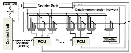
The proposed flexible accelerator architecture is shown in Fig. 1. Each FCU operates directly on CS operands and produces data in the same form1 for direct reuse of intermediate results. Each FCU operates on 16-bit operands. Such a bit-length is adequate for the most DSP datapaths , but the architectural concept of the FCU can be straightforwardly adapted for smaller or larger bit-lengths. The number of FCUs is determined at design time based on the ILP and area constraints imposed by the designer. The CStoBin module is a ripple-carry adder and converts the CS form to the two’s complement one.
The register bank consists of scratch registers and is used for storing intermediate results and sharing operands among the FCUs. Different DSP kernels (i.e., different
register allocation and data communication patterns per kernel) can be mapped onto the proposed architecture using post-RTL datapath interconnection sharing techniques.
The control unit drives the overall architecture (i.e., communication between the data port and the register bank, configuration words of the FCUs and selection signals for the multiplexers) in each clock cycle.
Fig 1 : Abstract form of the Flexible Datapath
A. Structure of the Proposed Flexible Computational Unit
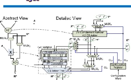
The structure of the FCU (Fig. 2) has been designed to enable high-performance flexible operation chaining based on a library of operation templates. Each FCU can be configured to any of the T1–T5 operation templates shown in Fig. 3. The proposed FCU enables intratemplate operation chaining by fusing the additions performed before/after the multiplication &performs any partial operation template of the following complex operations:
W* = A × (X* + Y*) + K* (1)
W* = A × K* + (X* + Y*) (2)
Fig 2: Flexible Computational Unit
The alternative execution paths in each FCU are specified after properly setting the control signals of the multiplexers MUX1 and MUX2 (Fig. 2). The multiplexer MUX0 outputs Y* when CL0 = 0 (i.e., X* + Y* is carried out) or Y* when X* − Y* is required and CL0 = 1. The two’s complement 4:2 CS adder produces the N* = X* + Y* when the input carry equals 0 or the N* = X* − Y* when the input carry equals 1. The MUX1 determines if N* (1) or K* (2) is multiplied with A. The MUX2 specifies if K* (1) or N* (2) is added with the multiplication product. The multiplexer MUX3 accepts the output of MUX2 and its 1’s complement and outputs the former one when an addition with the multiplication product is required (i.e., CL3 = 0) or the later one when a subtraction is carried out (i.e., CL3 = 1). The 1-bit ace for the subtraction is added in the CS adder tree.
The multiplier comprises a CS-to-MB module, which adopts a recently proposed technique to recode the 17-bit P* in its respective MB digits with minimal carry propagation. The multiplier’s product consists of 17 bits. The multiplier includes a compensation method for reducing the error imposed at the product’s accuracy by the truncation technique. However, since all the FCU inputs consist of 16 bits and provided
that there are no overflows, the 16 most significant bits of the 17-bit W* (i.e., the output of the Carry-Save Adder (CSA) tree, and thus, of the FCU) are inserted in the appropriate FCU when requested.
B. DFG Mapping Onto the Proposed FCU-Based Architecture
(A) (B)
Fig.3. Typical chaining of addition– multiplication–addition operations reflecting T1 template of Fig. 3. Its design is based on (A) CS optimizations with multiplication distribution (B) incorporating the CS-to-MB recoding concept.
IV. SIMULATION RESULTS
FIG.4 RTL SCHEMATIC
FIG.5 OUTPUT WAVEFORM
V. CONCLUSION
In this brief, we introduced a flexible accelerator architecture that exploits the incorporation of CS arithmetic optimizations to enable fast chaining of additive and multiplicative operations. The proposed flexible accelerator architecture is able to operate on both conventional two’s complement and CS-formatted data operands, thus enabling high degrees of computational density to be achieved. Theoretical and experimental analyses have shown that the proposed solution forms an efficient design tradeoff point delivering optimized latency/area and energy implementations.
EXTENSION
WORK:-As an extension we are implementing the DADDA Multiplier Using instead of Modified Booth Multiplier.
[1] P. Ienne and R. Leupers, Customizable Embedded Processors: Design Technologies and Applications. San Francisco, CA, USA: Morgan Kaufmann, 2007.
[2] P. M. Heysters, G. J. M. Smit, and E. Molenkamp, ―A flexible and energy-efficient coarse-grained reconfigurable architecture for mobile systems,‖ J. Supercomput., vol. 26, no. 3, pp. 283–308, 2003.
[3] B. Mei, S. Vernalde, D. Verkest, H. D. Man, and R. Lauwereins, ―ADRES: An architecture with tightly coupled VLIW processor and coarse-grained reconfigurable matrix,‖ in Proc. 13th Int. Conf. Field Program. Logic Appl., vol. 2778. 2003, pp. 61–70.
[4] M. D. Galanis, G. Theodoridis, S. Tragoudas, and C. E. Goutis, ―A high-performance data path for synthesizing DSP kernels,‖ IEEE Trans. Comput.-Aided Design Integr. Circuits Syst., vol. 25, no. 6, pp. 1154– 1162, Jun. 2006.
[5] K. Compton and S. Hauck, ―Automatic design of reconfigurable domainspecific flexible cores,‖ IEEE Trans. Very Large Scale Integr. (VLSI) Syst., vol. 16, no. 5, pp. 493–503, May 2008.
[6] S. Xydis, G. Economakos, and K. Pekmestzi, ―Designing coarse-grain reconfigurable architectures by inlining flexibility into custom arithmetic data-paths,―Integr., VLSI J., vol. 42, no. 4, pp. 486–503, Sep. 2009.
[7] S. Xydis, G. Economakos, D. Soudris, and K. Pekmestzi, ―High performance and area efficient flexible DSP datapath synthesis,‖ IEEE Trans. Very Large Scale
Integr. (VLSI) Syst., vol. 19, no. 3, pp. 429–
442, Mar. 2011.
[8] G. Ansaloni, P. Bonzini, and L. Pozzi, ―EGRA: A coarse grained reconfigurable architectural template,‖ IEEE Trans. Very
Large ScaleIntegr. (VLSI) Syst., vol. 19, no.
6, pp. 1062–1074, Jun. 2011.
[9] M. Stojilovic, D. Novo, L. Saranovac, P. Brisk, and P. Ienne, ―Selective flexibility: Creating domain-specific reconfigurable arrays,‖ IEEE Trans. Comput.-Aided Design Integr. Circuits
Syst., vol. 32, no. 5, pp. 681–694,
May 2013.