N A N O E X P R E S S
Open Access
Dislocation reduction of InAs nanofins prepared
on Si substrate using metal-organic vapor-phase
epitaxy
Chao-Wei Hsu
*, Yung-Feng Chen and Yan-Kuin Su
*Abstract
InAs nanofins were prepared on a nanopatterned Si (001) substrate by metal-organic vapor-phase epitaxy. The threading dislocations, stacked on the lowest-energy-facet plane {111}, move along the SiO2walls, resulting in a dislocation reduction, as confirmed by transmission electron microscopy. The dislocations were trapped within a thin InAs epilayer. The obtained 90-nm-wide InAs nanofins with an almost etching-pit-free surface do not require complex intermediate-layer epitaxial growth processes and large thickness typically required for conventional epitaxial growth.
Keywords:Threading dislocations, Metal-organic vapor-phase epitaxy, InAs, Nanofins
Background
The semiconductor industry has followed Moore's law for over 30 years with gate dimensions of transistors approaching the nanometer scale (<100 nm) [1]. The nanofin channels that are partly wrapped around these gates offer more effective control than that in traditional planar devices [2]. InAs is a direct-bandgap transition semiconductor material with high electron mobility [1-4]. InAs on a Si substrate is expected to allow side-by-side integration of InAs optoelectronics with conventional Si-based complementary metal oxide semiconductor products using monolithic epitaxial technology [1-8]. Un-fortunately, the hetero-epitaxy of InAs nanofins deposited on Si presents challenges, including the dislocations on the nanofin surface and positioning of the nanofin. These dislocations are generated due to an 11.6% lattice constant mismatch (aSi = 5.43 Å,aInAs= 6.06 Å), thermal expan-sion coefficient mismatch, and polarity mismatch [6-8]. For a zinc-blende structure deposited on a diamond struc-ture, the dislocations generated near the InAs/Si interface, such as mistfit dislocations, threading dislocations, and antiphase domain boundaries, are annihilated or multi-plied during the epitaxial process [6-19]. A previous report
indicated that a threading dislocation density above 107 cm−2for a 900-nm-thick epilayer decreased to 106cm−2 due to the self-annihilation of dislocations when the film thickness was increased to more than 4μm for a III-V epi-layer deposited on a Si substrate [8,18]. A III-V epiepi-layer on a miscut Si (001) substrate has fewer threading disloca-tions and antiphase domain boundaries than those of an epilayer on an untilted Si (001) substrate [6,17]. Previous studies have attempted to reduce the dislocation density for a III-V epilayer deposited on a Si (001) substrate using methods such as thermal cycle annealing and the utilization of short-period strained intermediate-layer superlattices [6-10]. During thermal cycle annealing treatment, an epilayer is subjected to large temperature oscillations and thus periodically switches between the compressed and tensile states, reversing the motion of the dislocations. However, thermal cycle annealing processes are time-consuming. Strained intermediate-layer superlat-tices effectively decrease the threading dislocation density by generating additional stress, but their insertion leads to poor reproduction. In previous reports, the density of dis-locations in an epilayer deposited on a planar Si substrate could be decreased by about two orders of magnitude by mixed thermal cycle annealing steps and strained intermediate-layer superlattice epitaxial growth processes [6-10]. An alternative technology for effectively reducing dislocation density is a kind of selective epitaxial growth
* Correspondence:[email protected];[email protected]
Department of Electrical Engineering & Advanced Optoelectronic Technology Center, Institute of Microelectronics, National Cheng Kung University, 1 University Rd, Tainan City 701, Taiwan
on patterned Si substrate, which has the capability to pro-duce a low-threading-dislocation surface using a simple epitaxial growth process. Yamaguchi et al. reported a model for the etching-pit density that could be reduced as the pattern trench width decreases [19].
In this work, InAs nanofins were deposited on nano-patterned Si (001) with SiO2as sidewalls. As confirmed by transmission electron microscopy (TEM), the high-aspect-ratio (aspect ratio = trench height / trench width) SiO2 sidewalls produce an almost etching-pit-free InAs surface. The 90-nm-wide InAs nanofins with almost etching-pit-free surfaces represent a breakthrough for a III-V material for use in the advanced Si-based semicon-ductor industry.
Methods
InAs nanofin growth was performed in an Aixtron (Herzogenrath, Germany) metal-organic vapor-phase epitaxy reactor using H2as the carrier gas, with a total flow of 6,000 sccm. A nanoscale shallow trench isola-tion pattern, with the narrowest width below 100 nm, and a miscut of 6° towards the 1 1 0 direction on p-type Si (001) wafers were adopted in this work. For patterned substrate fabrication, a 235-nm-thick SiO2film was formed by thermal oxidation on a Si (001) substrate. The SiO2 mask patterns were produced using 193-nm immersion lithography and reactive ion beam etching on a (001)-oriented Si substrate. The nanopatterned Si substrates were then cleaned in a 1:1:7 solution of reagent-grade HCl/ H2O2/H2O for 5 min prior to 1 vol.% HF for 1 min. After a thermal desorption procedure, low-temperature InAs nu-cleation layers were selectively grown on a patterned Si (001) substrate at 623 K and a pressure of 37.5 Torr. High-temperature InAs buffer layers were then selectively grown at 823 K and a pressure of 75.0 Torr. The surface mor-phology was studied using field-emission scanning electron microscopy (SEM). High-resolution cross-sectional TEM images were obtained using an FEI Tecnai F20 microscope (FEI, Hillsboro, OR, USA) operated at 200 kV.
Results and discussion
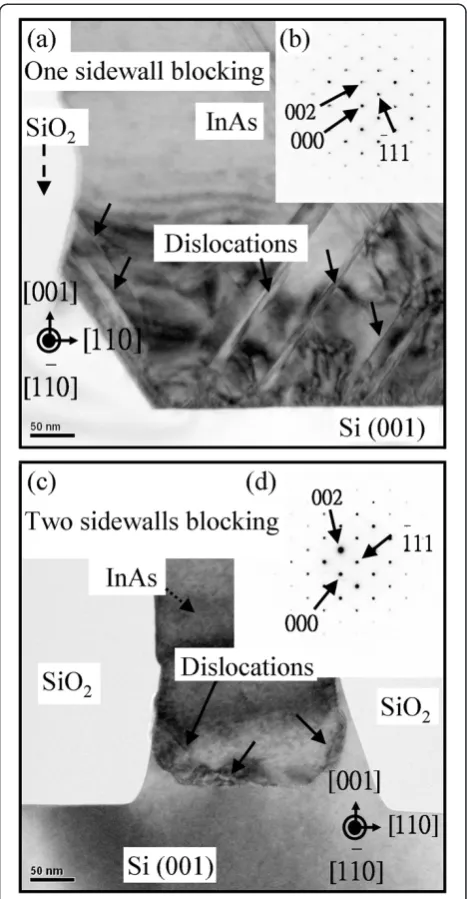
Figure 1a,b shows a cross-sectional TEM image and the diffraction pattern of InAs deposited on a one-SiO2-sidewall-patterned Si (001) substrate, respect-ively. The lattice constant of the InAs epilayer is about 5.96 Å. The arrows indicate the threading dis-locations. A large number of dislocations were gener-ated at the InAs/Si interface; the dislocation density is above 109 cm−2. In Figure 1a, the dislocations settle at an incline angle to the Si (001) surface, and some dislocations are blocked by the one-SiO2-sidewall pat-tern. However, this one-SiO2-sidewall pattern cannot effectively prevent the dislocations from prorogating
upward. Figure 1c shows a TEM image of InAs grown on a 200-nm-wide patterned Si (001) substrate with an aspect ratio of 1.2. The dislocations are blocked within the initial epilayer with the two-SiO2-sidewall-patterned Si substrate. The diffraction pattern of the InAs epilayer on a 200-nm-wide trench-patterned Si (001) substrate is shown in Figure 1d. The lattice constant is about 6.03 Å, which is similar to that of natural InAs (6.06 Å).
[image:2.595.305.539.88.538.2]The d002 value (d002 = 3.029 Å) of InAs on
Figure 1One-sidewall and two-sidewall blocking. (a)
nanopatterned Si substrate is similar to that of normal InAs (d002 = 3.030 Å). A low-residual-strain InAs epi-layer was obtained using the nanopatterned Si substrate. In addition, the diffraction pattern shows no twin spots, confirming a lack of twin defects. According to the dif-fraction pattern, the epitaxial direction of InAs is along the [001] direction. The InAs has a coherent direction with the (001)-oriented Si substrate.
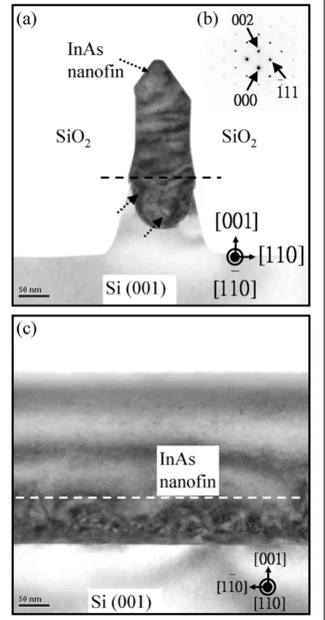
[image:3.595.306.539.94.538.2]Figure 2a,b shows a TEM image and the diffraction pattern of InAs grown on a 90-nm-wide trench-patterned Si (001) substrate with an aspect ratio of 2.5, respectively. The 110 direction is the short axis of the InAs nanofins. The lattice constant of the InAs epilayer is about 6.04 Å. Trenches with an aspect ratio of 2.5 are effective in stop-ping the extension of dislocations. The dislocations gener-ated in the zinc-blende (InAs) and diamond structure (Si) interface include misfit and threading dislocations. Misfit dislocations are generated from the InAs/Si interface and are parallel to the growth plane [15]. Theoretical models have proposed the possibility of strain relief by decreasing the initiating epitaxial areas to the nanoscale regime [19-24]. The effect of strain transfer and dilution for finite dimensional nanopatterned substrate is considered as the linear dimension of individual nanoscale areas is reduced to the point where the stress is completely relieved before sufficient energy is accumulated to create a dislocation. The almost dislocation-free epilayer is possibly demon-strated when the epilayer was deposited on a nanoscale epitaxial area. However, we observed the dislocations, as shown in Figure 2a. The stain energy in the trench middle region is higher than the trench edge region [20-23]. The dislocations are generated in the trench middle region due to strain relaxation. Then, the dislocations extended to the trench edge region. Figure 2c shows a cross-sectional TEM image along the 110 direction of the sample in Figure 2a. The 110 direction is the long axis of the InAs nanofins. The dislocations are trapped within the initial epilayer. It is anticipated that the upward propagation dis-locations are along the 110 direction (the short axis of the nanofins). Park et al.reported misfit segments mostly along the 110 direction (the short axis of the nanofins) for the epilayer deposited on submicron-patterned Si (001) substrate [25]. Misfit segments can lie along the
110
direction in the (001) growth plane, while threading segments rise up on the {111} plane in the same direction [6,25]. Threading dislocations on the {111} plane are a re-sult of the planes' lower facet surface energy [13,14]. Threading dislocations make a 45° angle with the under-lying Si (001) substrate. The threading dislocations can be stopped by the SiO2sidewalls on the Si (001) substrate. It is anticipated that almost all the dislocations will be blocked when the aspect ratio is greater than tan45° (as-pect ratio > 1 [width × tan45°]). For InAs deposited on a
90-nm-wide trench-patterned Si (001) substrate, the dislocations can be trapped at a thickness below approxi-mately 90 nm. As shown in Figure 2c, a displacement-type moiré pattern of the InAs initial deposition layer, which reflects the usual characteristic of a regular misfit direction, is observed at the InAs/Si interface. The InAs deposited on the nanopatterned Si (001) is almost dislocation-free on the top epilayer region. The pattern
aspect ratio of 2.5 is good enough to block the dislocations from propagating upward.
A schematic diagram of the dislocation-trapping mechan-ism is shown in Figure 3. Compared with the rectangular-planar-shaped trench bottom, the concave-shaped trench bottom helps the formation of double steps, resulting in the suppression of antiphase domain boundaries [12]. The concave-shaped bottom, related to the double-step forma-tion energetics on the substrate surface, facilitates surface step creation. Compared with InAs on a Si (111) substrate for a large number of vertical upward dislocations, the InAs on a Si (001) substrate can avoid the vertical upward dislo-cations. Compared to a one-SiO2-sidewall-patterned Si sub-strate, a high-aspect-ratio nanopatterned Si substrate with two SiO2 sidewalls can decrease the dislocation density from about 109cm−2to almost 0.
In previous reports, the etching-pit density of the epi-layer deposited on a planar Si substrate was reduced by more than one order of magnitude to about 1.2 × 106cm−2 using thermal cycle annealing and strained intermediate-layer superlattices [9,10]. Another study reported an etching-pit density of 2 × 106cm−2for epilayer deposited on a planar Si substrate using GeSi intermediate layers [26]. Another study found an etching-pit density for an epilayer deposited on submicron domain-patterned and planar Si substrates of 6 × 10⁵and 4 × 107cm−2, respectively [27]. The molten KOH etching was used to examine the disloca-tion behavior on the epilayer surface [15,28,29]. In this study, the samples were immersed in molten KOH solution at 633 K for 2 min, and then, the standard cleaning steps were used to clean the sample surface. Figure 4a shows a
[image:4.595.307.539.296.684.2]SEM image of an InAs nanofin surface. The InAs nanofin was selectively deposited in individual open Si surfaces bounded by the SiO2mask. The length of the nanofins is above 4.5 μm. A high-resolution TEM image of the InAs nanofin surface is shown in Figure 4b. The two images indicate an almost etching-pit-free InAs nanofin surface. Corresponding to Figure 2a,c, the dislocations generated from the InAs/Si interface were trapped, and thus, an al-most etching-pit-free surface was created, as shown in Figure 4a,b. Gao et al.reported vertical InP nanowires epi-taxially grown on Si (111) by metal-organic vapor-phase epitaxy (MOVPE) [30]. Liquid indium droplets were formed in situ and used to catalyze deposition. Recently, Miao et al. demonstrated a catalyst-free InP nanowire growth on Si (001) by MOVPE [31]. The density and size of the nanowires can be controlled, but the positions of the
Figure 3Principle of the dislocation-trapping mechanism and the almost dislocation-free top epilayer region.
Figure 4The 90-nm-wide InAs nanofins on nanopatterned Si substrate.SEM(a)and high-resolution TEM(b)images of the 90-nm-wide InAs nanofins on nanopatterned Si substrate with SiO2
[image:4.595.57.292.474.706.2]nanowires are difficult to define. In this study, we used the immersion lithography technique to define the nanoscale epitaxial position. InAs nanofins (a nanostructure similar to nanowires) on a nanopatterned Si (001) substrate are suit-able for the advanced commercial integrated circuit indus-try. InAs deposited on a nanopatterned Si substrate is a viable option for a good template for III-V epilayer inte-grated circuits for use with Si-based systems.
Conclusions
The 90-nm-wide InAs nanofins were selectively depos-ited on a nanopatterned Si (001) substrate with SiO2as sidewalls. As confirmed by TEM, the InAs deposited on the nanopatterned Si (001) shows an almost dislocation-free top epilayer region. The dislocations, originating from the InAs/Si interface, extended along the {111} facet plane and were terminated by two SiO2sidewalls. When the aspect ratio is greater than 1, the dislocations can be trapped within an initial thickness (thickness < 100 nm). The 90-nm-wide InAs nanofin surface is al-most etching-pit-free. InAs nanofins, with a width of about 90 nm, have the potential to be incorporated into the advanced Si-based complementary metal oxide semi-conductor technology platform, allowing InAs material to be integrated with Si (001) substrates.
Competing interests
The authors declare that they have no competing interests.
Authors’contributions
C-WH participated in the material preparation and data analysis and drafted the manuscript. Y-KS conceived of and co-wrote the paper. Y-FC participated in the sample characterization. All authors read and approved the final manuscript.
Authors’information
C-WH and Y-FC are postdoctoral researchers in the Institute of Microelectronics and the Department of Electronic Engineering, National Cheng Kung University, Tainan, Taiwan. Y-KS is currently a professor in the Institute of Microelectronics and the Department of Electrical Engineering, National Cheng Kung University, Tainan, Taiwan. Y-KS has authored or co-authored over 200 papers in the fields of thin-film materials, compound semiconductors, integrated optics, and optoelectronic devices.
Acknowledgements
The authors are grateful to Taiwan Semiconductor Manufacturing Company (TSMC) for its assistance. The authors thank the National Science Council and Bureau of Energy, Ministry of Economic Affairs of Taiwan for the financial support under contract no. NSC 101D02046 and the LED Lighting Research Center of NCKU for its assistance.
Received: 22 August 2012 Accepted: 21 October 2012 Published: 23 November 2012
References
1. Chau R, Datta S, Doczy M, Doyle B, Jin B, Kavalieros J, Majumdar A, Metz M, Radosavljevic M:Benchmarking nanotechnology for high-performance and low-power logic transistor applications.IEEE Trans Nanotechnol2005,
4:153–158.
2. Blekker K, Münstermann B, Matiss A, Do QT, Regolin I, Brockerhoff W, Prost W, Tegude F-J:High-frequency measurements on InAs nanowire field-effect transistors using coplanar waveguide contacts.IEEE Trans Nanotechnol2010,9:432–437.
3. Datta S, Dewey G, Fastenau JM, Hudait MK, Loubychev D, Liu WK, Radosavljevic M, Rachmady W, Chau R:Ultrahigh-speed 0.5 V supply voltage In0.7Ga0.3As quantum-well transistors on silicon substrate.IEEE Electron Device Lett2007,28:685–687.
4. Ihn SG, Song JI, Kim YH, Lee JY, Ahn IH:Growth of GaAs nanowires on Si substrates using a molecular beam epitaxy.IEEE Trans Nanotechnol2007,
6:384–389.
5. Soci C, Bao XY, Aplin DPR, Wang D:A systematic study on the growth of GaAs nanowires by metal-organic chemical vapor deposition.Nano Lett
2008,8:4275–4282.
6. Fang SF, Adomi K, Iyer S, Morkoç H, Zabel H, Choi C, Otsuka N:Gallium arsenide and other compound semiconductors on silicon.J Appl Phys
1990,68:R31–R58.
7. Yonezu H:Control of structural defects in group III–V–N alloys grown on Si.Semicond Sci Technol2002,17:762–768.
8. Bolkhovityanov YB, Pchelyakov OP:GaAs epitaxy on Si substrates: modern status of research and engineering.Phys Usp2008,51:437–456. 9. Takano Y, Hisaka M, Fujii N, Suzuki K, Kuwahara K, Fuke S:Reduction of
threading dislocations by InGaAs interlayer in GaAs layers grown on Si substrates.Appl Phys Lett1998,73:2917–2919.
10. Hayafuji N, Miyashita M, Nishimura T, Kadoiwa K, Kumabe H, Murotani T:
Effect of employing positions of thermal cyclic annealing and strained-layer superlattice on defect reduction in GaAs-on-Si.Jpn J Appl Phys1990,
29:2371–2375.
11. Cho N-H, De Cooman BC, Carter CB, Fletcher R, Wanger DK:Antiphase boundaries in GaAs.Appl Phys Lett1985,47:879–881.
12. Wang G, Leys MR, Loo R, Richard O, Bender H, Waldron N, Brammertz G, Dekoster J, Wang W, Seefeldt M, Caymax M, Heyns MM:Selective area growth of high quality InP on Si (001) substrates.Appl Phys Lett2010,
97(121913):1–3.
13. Morales FM, García R, Molina SI, Aouni A, Postigo PA, Fonstad CG:
Microstructure improvements of InP on GaAs (001) grown by molecular beam epitaxy byin situhydrogenation and postgrowth annealing.Appl Phys Lett2009,94(041919):1–3.
14. Usui H, Yasuda H, Mori H:Morphology and lattice coherency in GaAs nanocrystals grown on Si(001) surface.Appl Phys Lett2006,
89(173127):1–3.
15. Ishida K, Akiyama M, Nidhi S:Misfit and treading dislocations in GaAs layers grown on Si substrates by MOCVD.Jpn J Appl Phys1987,
26:L163–L165.
16. Otsuka N, Choi C, Nakamura Y, Nagakura S, Fischer R, Peng CK, Morkoç H:
High resolution electron microscopy of misfit dislocations in the GaAs/Si epitaxial interface.Appl Phys Lett1986,49:277–279.
17. Sieg RM, Ringel SA, Ting SM, Fitzgerald EA, Sacks RN:Anti-phase domain-free growth of GaAs on offcut (001) Ge wafer by molecular beam epitaxy with suppressed Ge outdiffusion.J Electon Mater1998,
27:900–907.
18. Wang G, Loo R, Simoen E, Souriau L, Caymax M, Heyns MM, Blanpain B:A model of threading dislocation density in strain-relaxed Ge and GaAs epitaxial films on Si (100).Appl Phys Lett2009,94(102115):1–3. 19. Yamaguchi M:Dislocation density reduction in heteroepitaxial III–V
compound films on Si substrates for optical devices.J Mater Res1991,
6:376–384.
20. Luryi S, Suhir E:New approach to the high quality epitaxial growth of lattice-mismatched materials.Appl Phys Lett1986,49:140–142. 21. Huang FY:Theory of strain relaxation for epitaxial layers grown on
substrate of finite dimension.Phys Rev Lett2000,85:784–787.
22. Fischer A, Richter H:Elastic misfit stress relaxation in heteroepitaxial SiGe/ Ge mesa structures.Appl Phys Lett1992,61:2656–2658.
23. Zubia D, Hersee SD:Nanoheteroepitaxy: the application of nanostructuring and substrate compliance to the heteroepitaxy of mismatched semiconductor materials.J Appl Phys1999,85:6492–6496. 24. Jain SC, Willander M, Maes H:Stresses and strains in epilayers, stripes and
quantum structures of III–V compound semiconductors.Semicond Sci Technol1996,11:641–671.
25. Park S-J, Bai J, Curtin M, Adekore B, Carroll M, Lochtefeld A:Defect reduction of selective Ge epitaxy in trenches on Si(001) substrates using aspect ratio trapping.Appl Phys Lett2007,90(052113):1–3.
27. Vanamu G, Datye AK, Dawson R, Zaidi SH:Growth of high-quality GaAs on Ge/Si1−xGexon nanostructured silicon substrates.Appl Phys Lett2006, 88(251909):1–3.
28. Shimizu M, Enatsu M, Furukawa M, Mizuki T, Sakurai T:Dislocation-density studies in MOCVD GaAs on Si substrates.J Crystl Growth1988,
93:475–480.
29. Wellmann PJ, Sakwe SA, Oehlshläger F, Hoffmann V, Zeimer U, Knauer A:
Determination of dislocation density in MOVPE grown GaN layers using KOH defect etching.J Crystl Growth2008,310:955–958.
30. Gao L, Woo RL, Liang B, Pozuelo M, Prikhodko S, Jackson M, Goel N, Hudait MK, Huffaker DL, Goorsky MS, Kodambaka S, Hicks RF:Self-catalyzed epitaxial growth of vertical indium phosphide nanowires on silicon. Nano Lett2009,9:2223–2228.
31. Miao G, Zhang D:Stages in the catalyst-free InP nanowire growth on silicon (100) by metal organic chemical vapor deposition.Nano Res Lett
2012,7(321):1–6.
doi:10.1186/1556-276X-7-642
Cite this article as:Hsuet al.:Dislocation reduction of InAs nanofins prepared on Si substrate using metal-organic vapor-phase epitaxy.
Nanoscale Research Letters20127:642.
Submit your manuscript to a
journal and benefi t from:
7 Convenient online submission 7 Rigorous peer review
7 Immediate publication on acceptance 7 Open access: articles freely available online 7 High visibility within the fi eld
7 Retaining the copyright to your article