warwick.ac.uk/lib-publications
Original citation:
Al-Amin, Mohammad and Murphy, John D.. (2017) Combining low-temperature gettering
with phosphorus diffusion gettering for improved multicrystalline silicon. IEEE Journal of
Photovoltaics, 7 (6). 1519 -1527.
Permanent WRAP URL:
http://wrap.warwick.ac.uk/91244
Copyright and reuse:
The Warwick Research Archive Portal (WRAP) makes this work of researchers of the
University of Warwick available open access under the following conditions.
This article is made available under the Creative Commons Attribution 3.0 (CC BY 3.0) license
and may be reused according to the conditions of the license. For more details see:
http://creativecommons.org/licenses/by/3.0/
A note on versions:
The version presented in WRAP is the published version, or, version of record, and may be
cited as it appears here.
Combining Low-Temperature Gettering With
Phosphorus Diffusion Gettering for Improved
Multicrystalline Silicon
Mohammad Al-Amin
and John D. Murphy
Abstract—We have investigated low-temperature (ࣘ500 °C) gettering in combination with phosphorus diffusion gettering with a view to improving poor quality multicrystalline silicon. Low-temperature gettering applied after standard phosphorus diffusion gettering is found to provide a>40% improvement in minority carrier lifetime in samples from the top and bottom of an ingot. The best results are achieved at 300°C with very long annealing times (>24 h). Improvements in the lifetime do not cor-relate with changes in interstitial iron concentration. Experiments are performed to assess whether the presence of a phosphorus-diffused emitter affects low-temperature gettering, and results from sister samples show the low-temperature gettering behavior is not affected by the existence of an emitter. Further experiments show that low-temperature gettering prior to phosphorus diffu-sion results in a 20% higher lifetime after phosphorus diffudiffu-sion. Low-temperature gettering can, therefore, enhance lifetime even when used in conjunction with standard phosphorus diffusion gettering.
Index Terms—Diffusion, gettering, iron, lifetime, multicrys-talline.
I. INTRODUCTION
M
ULTICRYSTALLINE silicon (mc-Si) contains both structural crystal defects (grain boundaries and dislo-cations) and impurity-related defects including point-like de-fects and precipitates. Impurities can interact with structural defects by segregation to their associated strain fields. Impuri-ties in the bulk, or when segregated to or precipitated at struc-tural defects, are often associated with recombination activity and thus degrade the minority carrier lifetime (henceforth re-ferred to as just “lifetime”). Transition metal impurities have particularly detrimental effects, yet many transition metals areManuscript received May 25, 2017; revised July 18, 2017 and August 8, 2017; accepted August 12, 2017. Date of publication September 6, 2017; date of current version October 19, 2017. This work was supported in part by the Engineering and Physical Sciences Research Council (EPSRC) under Grant EP/J01768X/2 and Grant EP/M024911/1, in part by the EPSRC Global Chal-lenges Research Fund under Grant EP/P511079/1, and in part by the Royal Society under Grant RG100076. The work of J. D. Murphy was supported by a Royal Academy of Engineering/EPSRC Research Fellowship. (Corresponding author: John D. Murphy.)
The authors are with the School of Engineering, University of Warwick, Coventry CV4 7AL, U.K. (e-mail: [email protected]; [email protected]).
Color versions of one or more of the figures in this paper are available online at http://ieeexplore.ieee.org.
Digital Object Identifier 10.1109/JPHOTOV.2017.2741100
sufficiently mobile that they diffuse during thermal processing. Gettering techniques are routinely used to improve mc-Si wafers by diffusing metallic impurities to near surface regions
(exter-nal gettering) or by re-arranging the impurities within the wafer
(internal gettering).
Gettering in mc-Si can be performed at low temperatures (<600°C) with improvements in a bulk lifetime [1], [2] and re-ductions in interstitial iron concentrations [1]–[5] having been achieved in as-grown wafers. Low-temperature gettering is pos-sible because the grown-in dissolved concentrations of impu-rities exceed their solid solubilities and this provides a ther-modynamic driving force for gettering. The gettering which results can be internal and/or external, depending on the pre-existence of external gettering sinks. Kinetic requirements for low-temperature gettering can be satisfied by the use of rela-tively long processing times (several hours or even days). Such processing times may be satisfactory because usual cleanliness standards can be relaxed due to the low risk of external contam-ination. It is also noted that the required annealing conditions are not dissimilar to those used in other industries (e.g., in the toughening of glass).
Low-temperature gettering is simple in theory, but in reality, the processes involved are complex. Our previous detailed inves-tigations show that gettering in as-grown wafers is not limited only by impurity diffusion [1] (as suggested previously [3]) and also that the passivation used for lifetime measurement plays an important role [2]. External gettering to dielectrics used for lifetime measurement can also occur [5]. The gettering behav-ior is highly dependent on wafer microstructure, with internal gettering being more effective in wafers from the bottom of an ingot with a relatively low dislocation density than in top wafers with a relatively high dislocation density [1].
In the production of solar cells from p-type mc-Si substrates, a phosphorus diffusion at high temperatures (ࣙ800°C) is rou-tinely used to form an n-type emitter region at the surface. An important side effect of emitter formation is phosphorus diffu-sion gettering (PDG) of impurities [6]–[11]. PDG is a highly effective form of external gettering and can reduce bulk in-terstitial iron concentrations by more than 99% [8] with mod-ified PDG processes providing even more effective gettering [12]. While separate low-temperature gettering processes in as-grown mc-Si can provide substantial improvements in the lifetime [1],[2] and/or substantial reductions in interstitial iron concentration [1]–[5], it is not clear how these benefits are
1520 IEEE JOURNAL OF PHOTOVOLTAICS, VOL. 7, NO. 6, NOVEMBER 2017
affected by PDG which would necessarily occur in solar cell fabrication.
In this paper, we aim to investigate whether low-temperature gettering used either before or after a standard phosphorus dif-fusion step can result in a lifetime improvement. Some insight into this issue can be gained from the limited information in the previous related studies [13]–[16]. For example, Sch¨on et al. found that annealing at 550°C after PDG gave rise to a small increase in lifetime and a reduction in interstitial iron concen-tration by about one order of magnitude or more [15]. Boulfrad
et al. reported limited data on the impact of a 550°C pre-anneal prior to PDG, finding a lower lifetime and higher interstitial iron concentration in this wafer compared to a control which only underwent PDG [16]. Low-temperature gettering has also been applied at cell level by Rinio et al. [14] and Pickett and Buonas-sisi [13]. Both studies found improvements in cell efficiency relative to samples from a control process, with Rinio et al. con-cluding the improvement was most likely to result from external gettering of impurities to the emitter [14], [17]. Whilst the con-sensus is that low-temperature annealing after PDG can improve performance, detailed understanding of why this improvement occurs is hard to obtain from previous studies because of the methodologies used. For example, these previous studies [13]– [17] used dielectric surface passivation (possibly resulting in bulk hydrogenation [18]) and the competing effects of external (at the dielectric [5] or phosphorus-diffused region) and inter-nal gettering were not always isolated. When comparing other studies, it is also important to consider how the anneals were performed, as when low-temperature annealing is performed in the same furnace cycle as PDG, then there is often a slow cool-down before the low-temperature annealing and gettering can occur during this cooling step.
This paper reports the results of three carefully designed ex-periments, which intend to address three important questions regarding the relationship between PDG and low-temperature gettering in mc-Si. These are
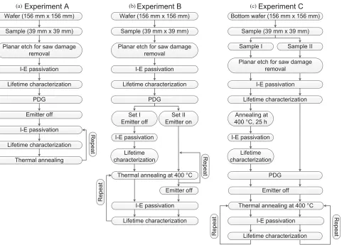
1) Can low-temperature gettering applied after PDG improve the properties of relatively poor lifetime wafers from the top and bottom of an ingot (Experiment A)?
2) Does low-temperature gettering after PDG arise from ex-ternal gettering to the emitter as proposed by Rinio et al. [14], [17] or internal gettering (Experiment B)?
3) Does any lifetime improvement resulting from low-temperature annealing before PDG carry forward into sub-sequent processing (Experiment C)?
The experimental methodology involves low-temperature (300°C to 500°C) processing of sister samples from adjacent wafers in the ingot with near-identical microstructures, starting lifetimes, and interstitial iron concentrations. The focus is on material from the top and bottom of a commercially grown in-got. Such wafers are typically classified as “red-zone” material as their lifetime is too low for the production of viable solar cells. To measure lifetimes and interstitial iron concentrations at each processing stage we use a temporary liquid surface passivation scheme, as this minimizes ambiguities due to probable hydro-genation and external gettering associated with dielectric-based passivation schemes.
II. EXPERIMENTALMETHODS
For all experiments, mc-Si samples measuring 39 mm×39 mm were taken from the top (T) and/or bottom (B) parts of a conventional (not “high performance”) directionally solidi-fied ingot. Microstructural characterization of samples from the same ingot has been published previously [1]. Samples were
p-type (boron doped, ∼1 Ω·cm). The key process steps are shown in Fig. 1 and details are given in the following sections.
A. Experiment A: Low-Temperature Annealing After PDG
This experiment was designed to investigate low-temperature gettering after a PDG process. Batches of sister samples from both height positions were first chemically polished with a pla-nar etch solution comprising HF (50%), HNO3 (69%), and CH3COOH (100%) in the ratio of 24:58:18 to remove saw damage. Samples were then cleaned using HCl and HF and subjected to a standard phosphorus diffusion process in a tube furnace using POCl3 at 840°C for 44 min at Universit¨at Kon-stanz, Germany. The loading and unloading temperatures were 800°C, and the loading and unloading temperature rates were several degrees per minute. The average sheet resistance of the emitter was∼55Ω/, measured with a four-point-probe. A so-lution of HNO3(69%):CH3COOH(100%):HF(50%) in the ratio 10:5:2 was used to remove∼5µm of material from both sides to ensure the emitter was no longer present. Average samples thicknesses were determined individually by weighing the sam-ples and were 100–140µm after etching. Samples were RCA cleaned and were then annealed at 300°C, 400°C, and 500°C under nitrogen ambient. Samples from both height positions were subjected to identical thermal and cooling treatments at a given temperature, as annealing and removal were performed simultaneously.
For characterization purposes, samples were passivated at each measurement stage with a temporary liquid iodine–ethanol (I–E) solution (0.1 M), as described previously [1]. Samples were characterized in the as-grown state and after every low-temperature annealing stage. After each measurement procedure sequence, great care was taken to clean residue of the I–E solu-tion from the surface. Lifetimes were measured at room temper-ature using quasi-steady-state photoconductance (QSS-PC) [19] with a Sinton WCT-120 lifetime tester and lifetimes are reported at an injection level of 1×1015cm–3. The reproducibility of the
I–E surface passivation has been checked in a series of control experiments on float-zone silicon samples. Measured lifetimes are consistent with the reproducibility found in the study of Blum et al. [20], so we take their value of within-laboratory standard deviation for QSS-PC lifetime measurement of±4.3% as the error in our measurements. The spatial distribution of life-time was measured using a BT Imaging LIS-L1 PL imaging tool calibrated with QSS-PC measurements. Two sets of measure-ments were made at each stage[one with bulk iron in the FeB state and one in the interstitial iron (Fei) state]. The bulk intersti-tial iron concentration was estimated from the QSS-PC data at an injection level of 1×1015cm–3using the approach described
Fig. 1. Process sequences for the three different experiments: (a) Experiment A which aims to assess the effect of low-temperature annealing after PDG; (b) Experiment B which aims to establish whether samples annealed with emitters undergo internal or external gettering; and (c) Experiment C which aims to investigate the potential of low-temperature gettering prior to PDG.
during measurement by the PL imaging technique. More details of characterization processes are given in our earlier paper [1].
All lifetimes reported here lie well above the detection limit of QSS-PC, which is typically <1 µs. The detection limit of interstitial iron measured by photodissociation of FeB pairs [22] depends on the absolute lifetime used in the calculation. At the injection level used (above the cross-over point [23]), an estimate of the detection limit can be obtained from calculating the interstitial iron concentration at which the upper bound FeB lifetime [20] overlaps with the lower bound Fei lifetime. The detection limit, therefore, varies point by point, so with the results of each experiment, we state the typical most relevant estimated detection limit for interstitial iron.
B. Experiment B: Effect of Phosphorus-Diffused Emitter on Low-Temperature Gettering
This experiment aims to assess whether any improvements in bulk lifetimes due to low-temperature annealing after PDG occur via external gettering to the emitter or via internal getter-ing. Sister samples from both height positions were subjected to saw damage removal, RCA cleaning, and the PDG process as described in Experiment A. One top and one bottom sample had the emitter layer removed prior to thermal annealing step, using
the method described above. The emitter was retained on both sides of the other sister top and bottom samples. All samples (with and without emitters) were subjected to annealing under nitrogen ambient at 400°C in stages to up to 50 h of cumulative time. After the final annealing step, the usual chemical treat-ment was used to remove the emitters remaining at the surfaces of the two samples on which the emitters had been retained. Samples at this stage were∼120µm thick. The same charac-terization methodology as in Experiment A was used, and it is noted that the samples for which emitters were retained during low-temperature annealing could only be accurately character-ized at the as-grown and final stages as Auger recombination in the highly doped emitter dominates effective lifetime [24].
C. Experiment C: Low-Temperature Gettering in Bottom Wafers Prior to and After PDG
1522 IEEE JOURNAL OF PHOTOVOLTAICS, VOL. 7, NO. 6, NOVEMBER 2017
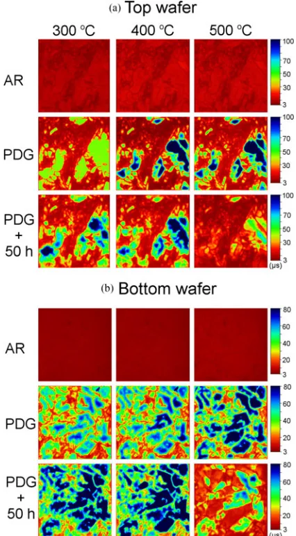
Fig. 2. Experiment A: effective minority carrier lifetime with iron in the FeB state measured by QSS-PC for samples from the top (T) and bottom (B) of the mc-Si ingot. Emitters were etched off prior to annealing at 300°C, 400°C, and 500°C for the cumulative annealing time period shown. The dashed lines represent the values immediately after PDG with the emitter etched off. The as-received state is denoted by AR.
first sample was subjected to a 25 h anneal at 400°C under ni-trogen ambient. These annealing conditions are known from our previous work [1] to give a substantial lifetime improvement. This pre-annealed sample and a second control sample were then subjected to the same PDG as in Experiment A. Emitter layers were removed from both samples as described previously and the samples (now with a thickness of∼120µm) were then annealed under nitrogen ambient at 400°C in stages up to a total of 41 h. I–E surface passivation was used when characterizing the samples using the methods in Experiment A at all possible processing steps.
III. RESULTS
A. Experiment A: Low-Temperature Annealing After PDG
[image:5.594.324.537.66.452.2]Fig. 2 shows the average bulk lifetime with iron in the FeB state as a function of cumulative annealing time at 300 °C, 400 °C, and 500°C. Starting lifetimes in the bottom and top samples are on average 6.1 and 11µs, respectively. After PDG, the average lifetime increases to 59µs for the bottom sample and 19 µs for the top sample. The post-PDG lifetime values are represented by the dashed lines plotted on every graph, as, in the case of Experiment A, the relevant change is that relative to this value. PDG lifetime is generally improved by annealing both bottom and top samples at 300°C and 400°C. For 50 h annealing, the largest improvement was found in a bottom sample annealed at 300°C (from 54 to 78µs). Lifetime changes after 50 h were+44% at 300°C and+36% at 400°C in bottom samples, and+48% at 300°C and+42% at 400°C in top samples. Some lifetimes measured for shorter annealing times were higher than the 50 h value (e.g., the bottom sample lifetime was increased by 71% after 26 h at 300°C). Annealing at 500°C decreased the lifetime in both samples, with the change after 50 h being –45% for the bottom sample and –20% for the top sample.
Fig. 3. Experiment A: spatial distribution of minority carrier lifetime with iron in the FeB state for sister samples from the (a) top and (b) bottom parts of the ingot at three key process stages as-received (AR), after phosphorus diffusion gettering with the emitter etched off (PDG), and after subsequent annealing at 300°C, 400°C, and 500°C for 50 h of cumulative time.
The spatial distribution of lifetime with iron in the FeB state at three key stages (as-received, PDG, and after the final post-PDG annealing step) for the samples from top and bottom sam-ples is presented in Fig. 3(a) and (b), respectively. As-received lifetimes are very low in both the bottom and top samples, with some grain boundaries exhibiting even lower lifetimes than the bulks of the grains. The PDG process has the effect of improving lifetime in the bulks of some of the grains and the lifetime in the vicinity of some grain boundaries is also improved. Annealing at 300°C and 400°C after PDG results in further improvements in both sample types. Annealing at 500°C after PDG reduces lifetime, reversing some of the beneficial effects on the lifetime of PDG in the bulks of the grains.
Fig. 4. Experiment A: bulk interstitial iron concentration ([Fei]) from QSS-PC measurement for samples from the top (T) and bottom (B) of the mc-Si ingot. Sister samples were gettered with phosphorus diffusion. Emitters were etched off prior to annealing at 300°C, 400°C, and 500°C for the cumulative annealing time period. The dashed lines represent the values after PDG with the emitter etched off. The as-received state is denoted by AR.
bottom samples and 1.1×1012cm–3in top samples. The PDG
process reduces the interstitial iron concentration by a factor of 35–54 for bottom samples and by a factor of 8–30 for top samples. The dashed lines in Fig. 4 represent the interstitial iron concentration after PDG and low-temperature annealing post-PDG does not generally reduce the concentration substantially. We have checked for a correlation between lifetime change and interstitial iron change but there does not seem to be a simple one. Surprisingly, interstitial iron concentrations appear even to increase slightly upon annealing at 400°C and 500°C for the top samples. We note that the typical interstitial iron concen-trations measured are above the lifetime-dependent detection limits which are typically around 3 ×1010 cm–3 for bottom
samples and 8×1010cm–3for top samples.
B. Experiment B: Effect of Phosphorus-Diffused Emitter on Low-Temperature Gettering
Fig. 5 shows a comparison in the bulk lifetime and bulk interstitial iron concentration for sister top and bottom samples annealed at 400°C with and without an emitter region at both surfaces. The lifetimes and interstitial iron concentrations in the as-received state and after the PDG are similar to those samples used in Experiment A, even though the samples were not part of the same sister set. Post-PDG annealing of bottom samples at 400°C ultimately improves lifetime marginally (from 39 to 44µs after 50 h) for samples from which the emitter had been removed. The sister sample, on which the emitter was retained during annealing, had a very similar final lifetime. The presence or absence of an emitter also made very little difference to the ultimate interstitial iron concentration in bottom samples. We note that the interstitial iron concentrations measured are generally above the detection limits which are conservatively estimated to be around 4×1010cm–3 for bottom samples and
around 6×1010cm–3 for top samples. The situation was less
clear-cut in top samples. The lifetime measured after 50 h of annealing at 400°C was similar to the lifetimes measured with
[image:6.594.52.276.66.220.2]Fig. 5. Experiment B: Effect of phosphorus-diffused layer in low-temperature gettering for samples from the top (T) and bottom (B) parts of the mc-Si ingot. Samples were annealed at 400°C for the cumulative annealing time period. Set I and II samples were annealed without and with phosphorus-diffused layer, respectively. The dashed lines represent the values after PDG without emitter. The as-received state is denoted by AR.
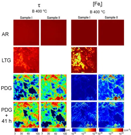
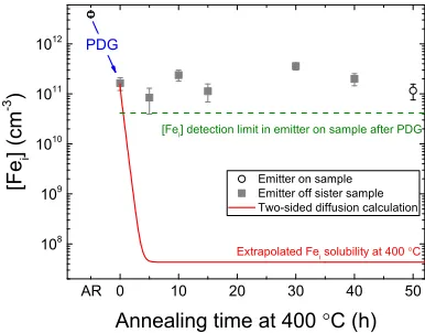
Fig. 6. Experiment C: a comparison of bulk lifetime and interstitial iron concentration in low-temperature gettering for samples from the bottom part of the ingot. Sample I was annealed at 400°C for 25 h prior to the PDG process. Samples I and II were annealed after PDG process at 400°C for the shown cumulative annealing time period. The labels represent the as-received state (AR), after low-temperature gettering (LTG) in the case of sample I, and after phosphorus diffusion gettering (PDG). The dashed lines represent the values after PDG with the emitter etched off.
the emitter removed for shorter time steps. The actual lifetime measured for 50 h in the top sample with the emitter removed took a lower value, but the reason for this is not clear. The interstitial iron concentration behaved in a corresponding way.
C. Experiment C: Low-Temperature Gettering in Bottom Wafers Prior to and After PDG
[image:6.594.314.538.296.473.2]1524 IEEE JOURNAL OF PHOTOVOLTAICS, VOL. 7, NO. 6, NOVEMBER 2017
Fig. 7. Experiment C: spatial distribution of minority carrier lifetime with iron in the FeB state for bottom samples at different key process stages such as as-received (AR), after first low-temperature gettering at 400°C for 25 h (LTG), after phosphorus diffusion gettering with the emitter etched off (PDG), and after subsequent annealing at 400°C for 41 h of cumulative time.
study [1]. After PDG, the lifetime is 82µs in sample I and 68
µs in sample II. Lifetimes measured after post-PDG annealing are fairly scattered.
Fig. 6 also shows the average as-received interstitial iron con-centration is 3.6×1012cm–3in both samples. In sample I, the
interstitial iron concentration decreases to 4.8×1011cm–3upon
annealing at 400°C for 25 h prior to PDG process. The PDG process further decreases the bulk interstitial iron concentration to 2.8×1010cm–3. The interstitial iron concentration immedi-ately after PDG in sample II is higher (1.4×1011 cm–3). For both samples, post-PDG annealing at 400°C does not further reduce the interstitial iron concentration significantly, consistent with results from Experiment A in Fig. 4. The detection limit for interstitial iron in these samples is around 2×1010cm–3or
better.
Fig. 7 shows the spatial distribution of lifetime and intersti-tial iron concentration at key stages for both the bottom samples used in Experiment C, and the same scales are used for both samples. As expected, lifetime is very low and interstitial iron concentration is high (>1 ×1012 cm–3) throughout the
sam-ples in the as-received states. In sample I, lifetime improves in most of the grains upon pre-PDG annealing. After PDG, lifetime increases in most of the grains. The interstitial iron concentra-tions decrease in some of the grains upon pre-PDG annealing (sample I) and reduce further in the PDG process. After post-PDG annealing at 400°C for 41 h, lifetime increases in some bulk grain regions and decreases or remains unchanged in most of the bulk grain regions.
IV. DISCUSSION
Throughout our discussion, it is important to note that our methodology based on I–E surface repassivation at each
characterization step avoids potential ambiguities that may be present in other studies which have used dielectric surface pas-sivation. The changes in properties we measure are dominated by thermal effects and impurity gettering, as bulk passivation arising from bulk hydrogenation (as suggested previously [18]) is not likely to have occurred to the extent it might have with di-electric passivation. Our experiments also could not have been affected by impurity gettering to the dielectric [5]. Previous work in single-crystal silicon has suggested interstitial iron get-tering to a surface only becomes kinetically dominated when a pre-existing sink exists at the surface [25], so in the cases of an emitter-free surface, we anticipate internal gettering to crys-tallographic defects to dominate over external gettering to free surfaces.
As a further general point, we note that the samples studied are typical of mc-Si from the bottom and top of a cast ingot, and that the PDG process used gave typical results. Figs. 2 and 4–6 show that the as-received bottom samples have lower average lifetime and higher interstitial iron concentration than those in top samples, which is consistent with our previous study [1]. The PDG process improves the bulk lifetimes and reduces inter-stitial iron concentration substantially in both the top and bottom samples. Interstitial iron concentrations are reduced by 97–98% in bottom samples, and 88–97% in top samples, and these re-ductions are broadly consistent with the findings in other PDG studies (e.g., [8]). We attribute the higher lifetime in gettered bottom samples to their lower density of dislocation clusters which, in many cases, remain recombination active after PDG [26]. We note dislocation density maps for samples from the same mc-Si ingot are published in [1].
The results of the three experiments are discussed in turn in the next three sections, and a final section reviews the status of low-temperature gettering in the context of cell processing.
A. Lifetime and Interstitial Iron with Post-PDG Low-Temperature Annealing (Experiment A)
The impact of low-temperature annealing on lifetime after PDG is shown in Fig. 2. As a general rule, it appears that lower temperatures are better than higher temperatures. Annealing at 300°C gives favorable results for both bottom and top samples in which the lifetimes after 50 h increase by 44% and 48%, respectively. The PL lifetime images (see Fig. 3) show the im-provements in lifetime arise in the bulks of certain grains. As was the case for as-received mc-Si [1], the low-temperature gettering process cannot be explained by a simple activation-energy-controlled diffusion process as the gettering effect does not improve with temperature.
to gettering of interstitial iron, but some other recombination-active defect whose identity is not currently known. Sch¨on et
al. reported a reduction in interstitial iron by more than one
order of magnitude after post-PDG low-temperature annealing at 550°C [15]. Our results do not find an improvement of this magnitude, but this discrepancy could be explained by their low-temperature annealing step being performed in situ after a relatively slow cool-down from the high-temperature stage. Furthermore, their samples were passivated with silicon ni-tride which may have resulted in bulk hydrogenation or external gettering.
Post-PDG annealing at 500°C generally has a negative im-pact on the lifetime (see Fig. 2). With the exception of bottom samples (in which there was a lot of interstitial iron to getter), this was the case in as-received samples too [1]. We note that recent work has shown that 500°C annealing can activate a re-combination center even in high-purity float-zone silicon which is probably related to vacancies [27], [28]. It is possible that this defect is activated in mc-Si too. It is also the case that the in-terstitial iron concentration increases slightly upon annealing at 500°C, and this phenomenon was observed in as-received mc-Si previously [1]. This would suggest that 500°C annealing is sufficient to release interstitial iron from another type of defect within the material. The possibility of external contamination has been ruled out by putting float-zone silicon controls through our process, as described previously [1].
Those who have used low-temperature annealing in cell pro-duction typically find improvements at higher temperatures than us. Pickett and Buonassisi found cell efficiency improvements to arise in mc-Si grown from iron-rich feedstock from relatively short annealing (30 min) at 500°C performed after phosphorus diffusion before the etch [13]. Details are limited, but it could be that their iron concentrations were substantially higher than ours and the higher iron levels resulted in different behaviors. Rinio
et al. found the best cell efficiency improvement at∼575 °C [14], but we note this was for edge samples from the middle of a block which would have had high contamination levels due to impurity in-diffusion from the crucible walls [29]. It, therefore, appears that low-temperature gettering is highly dependent on the specific properties of the wafers to which it is applied. As is the case for PDG processes [30], it appears that for opti-mal low-temperature gettering it is necessary to customize the thermal treatment according to properties of the material being processed.
B. Effect of Emitter in Post-PDG Low-Temperature Annealing (Experiment B)
[image:8.594.329.522.65.216.2]Fig. 5 shows the effective lifetime and interstitial iron concen-tration in sister samples subjected to post-PDG low-temperature gettering at 400°C. In one set of samples, the emitters were re-moved prior to low-temperature annealing and in the other set, the emitters were removed from both sides after low-temperature annealing. As the samples have near-identical microstructures and were thermally processed at the same time, we believe it is a reasonable assumption that the existence or nonexistence of the emitter is the only difference between the two cases. Fig. 5
Fig. 8. Experiment B: Experimentally measured bulk interstitial iron concen-tration in sister samples compared to a simulation of interstitial iron diffusion to both surfaces (thickness: 125µm). The interstitial iron, whilst above the estimated detection limit, does not behave as would be expected if it were get-tered to phosphorus-diffused emitters at both surfaces. The as-received state is denoted by AR.
shows the bottom samples annealed with and without emitters have very similar lifetimes and interstitial iron concentrations after annealing at 400°C for 50 h. The data for top samples in Fig. 5 are less convincing, but the emitter on measurement at 50 h is in good agreement with earlier emitter off times. If impurity gettering to the emitter were happening in top samples, then the lifetime would likely be significantly higher than at earlier times with the emitter and this is not what is observed.
It is noted that even after PDG, the interstitial iron level in the bulk massively exceeds the solid solubility at 400°C, and this should provide a thermodynamic driving force for gettering. However, it is known from our earlier work [1], [2] that inter-stitial iron levels in mc-Si without phosphorus-diffused layers do not decay as might be expected from previous studies in single crystal material (e.g., [25]). If the phosphorus-diffused emitter regions were to act as sites for gettering, then based on the known diffusion behavior of interstitial iron in single-crystal silicon (e.g., [31]), the long (50 h) annealing time used would be sufficient for interstitial iron to reach these regions even at 400 °C. To illustrate this point, Fig. 8 shows a comparison between selected experimental data for bottom samples from Fig. 5 and a calculation of interstitial iron transport to emitters at both surfaces. Details of the diffusion calculation have been published previously [25], and the curve plotted takes the diffu-sivity of interstitial iron in silicon at 400°C as 9.6×10⁻⁹cm2·s–1
[31], the sample thickness as 125µm (as measured before emit-ter removal), and the equilibrium inemit-terstitial iron concentration as 4.3×107cm–3(extrapolated from [32]). Fig. 8 clearly shows
the interstitial iron, whilst in excess of the detection limit, does not reduce in a way consistent with the expected diffusion to the emitter regions.
1526 IEEE JOURNAL OF PHOTOVOLTAICS, VOL. 7, NO. 6, NOVEMBER 2017
silicon. Our results appear to suggest that iron is trapped in the bulk in mc-Si. Whilst this is possible, it could also be the case that the relatively high levels of interstitial iron measured are some artifact of the measurement procedure. Studies into what determines the true interstitial iron detection limit and the pho-todissociation of other impurity-containing complexes in mc-Si should be the subject of further study. Aside from trapping, an-other explanation could be that iron is not sufficiently soluble in the phosphorus-diffused layer at low temperatures, but this can probably be ruled out because the segregation coefficient of iron into the phosphorus-doped layer increases with decreasing temperature [33].
The findings of our Experiment B appear to contradict the conclusions of Rinio et al. [14], [17] who attributed their cell efficiency or lifetime improvements due to low-temperature an-nealing to external gettering to the emitter. Reasons for a differ-ence could be the different properties of the samples studied, or the slightly different temperatures used.
C. Effect of Pre-PDG and Post-PDG Low-Temperature Gettering (Experiment C)
Experiment C was designed to establish whether low-temperature gettering prior to PDG improves lifetime after PDG. The results in Fig. 6 show the low-temperature gettering in sample I prior to PDG results in a lifetime improvement (factor of∼5.1) and interstitial iron reduction (factor of∼7.9) and this is broadly as expected from our previous study [1]. The subse-quent PDG process applied to sample I and sample II increased lifetime and reduced interstitial iron concentration in both cases. The lifetime after PDG in sample I was higher than in sample II (82µs compared to 68µs) and the interstitial iron concentration was lower (2.8×1010 cm–3compared to 1.4×1011cm–3). It,
therefore, appears that in this case, there is a small benefit in subjecting samples to low-temperature gettering prior to PDG. This can be seen from the lifetime images in Fig. 7.
Subsequent low-temperature gettering experiments were then performed on both sister samples at 400°C (see Fig. 6). The lifetime in the sample not subjected to a pre-PDG annealing (sample II) was increased slightly whereas sample I’s lifetime stayed fairly constant. Sample II’s relatively high interstitial iron concentration after PDG (perhaps due to incomplete gettering) was reduced. Thus, an improvement of similar (relatively small) magnitude can be achieved by performing the low-temperature annealing before or after PDG, with final lifetime images (see Fig. 7) showing similar distributions.
Our explanation of Experiment C is that the pre-PDG low-temperature gettering results in internal gettering of impurities including interstitial iron. This could be due to relatively spaced-out features such as grain boundaries or a low concentration of precipitates. The gettering rate for interstitial iron has previously been found to be slower than expected for gettering to surfaces [1], so dislocations are not a likely candidate for gettering as they are, on average, more closely spaced than surfaces. The internally gettered impurities are sufficiently stable that they survive the high-temperature PDG stage and the impurities are not released back into the bulk.
D. Prospects for Using Low-Temperature Gettering in Solar Cell Production
Prior work [1]–[5] has used low-temperature gettering on rel-atively poor as-grown mc-Si wafers, and significant improve-ments in the lifetime have been demonstrated [1], [2]. The aim of this paper was to address the interplay between low-temperature gettering and PDG. We have shown in Fig. 2 that that low-temperature gettering applied after a standard PDG process re-sults in gettering which gives lifetime improvements of>40% in relatively low lifetime samples from the top and bottom of the block. The times required to get these improvements are long (generally>24 h at 300°C), so whether such a process is viable is now a commercial question not a scientific one. It is important to note that relatively sophisticated diffusion furnaces are not required for the low-temperature annealing, so processes could be performed in relatively cheap large ovens instead.
Furthermore, it is also important to note that our conclusions here are based on data from samples passivated with I–E solution and not a dielectric layer which may be present at the surface of a part-processed solar cell. Hydrogen-rich SiNx grown by plasma-enhanced chemical vapor deposition is believed to in-troduce hydrogen into the wafer bulk [18]. Therefore, lifetime changes induced by low-temperature annealing of a part- or fully processed solar cell passivated with SiNx may be different to those we have observed due to modification of bulk passivation upon annealing. Others have studied how hydrogen charge-state manipulation at low temperatures can be used to control lifetime in silicon (e.g., [34]). Thus, whilst combining low-temperature annealing with PDG has at best only moderate benefits with regard to enhancing impurity gettering, low-temperature pro-cessing may help with hydrogen control.
One aspect that we have not yet addressed is the impact of a short firing anneal. Previous work has shown that substan-tial increases in interstisubstan-tial iron concentrations occur after short anneals of the kind used for contact firing [35]. Our results in Fig. 5 indicate that low-temperature gettering is not affected substantially by the presence of an emitter, so low-temperature annealing could be used for internal gettering of impurities re-leased during cell firing. The stability of the contacts under the relatively long times required for effective low-temperature get-tering would need assessing, however. Furthermore, there is a window of opportunity for low-temperature gettering in silicon photovoltaic devices which are not processed at the relatively high temperatures required for PDG (ࣙ800 °C). It is possi-ble, for example, that diffusionless heterojunction-based silicon solar cells made from high-performance mc-Si could use low-temperature gettering, hence enabling a cell which does not require any high-temperature processing.
V. CONCLUSION
gettering in wafers which have already undergone a phosphorus diffusion step. Our best results were achieved at 300 °C, for which lifetime improvements of>40% were achieved in low lifetime wafers from the bottom and top of a commercial block. Improvements are not found to correlate with interstitial iron concentration changes, so the gettering of a different defect (or defects) is occurring. In the second experiment (Experiment B), we studied the effect of the presence of an emitter during the low-temperature gettering step. We found no clear evidence that the emitter plays a role in the low-temperature gettering process, so we conclude that changes observed are most likely due to internal rather than external gettering. In the final experiment (Experiment C), we found that performing the low-temperature gettering step prior to PDG gives a∼20% higher lifetime than if the low-temperature step were not performed. It was also found that applying the low-temperature step after PDG gives the same ultimate lifetime result.
In summary, low-temperature gettering can improve minority carrier lifetime in mc-Si when applied appropriately in conjunc-tion with a standard phosphorus diffusion process. The anneal-ing times are long, however, (generally >24 h) and this may limit the commercial attractiveness of such processes.
ACKNOWLEDGMENT ANDACCESS TODATA
The authors are grateful to the group of Prof. G. Hahn (Universit¨at Konstanz, Germany) for performing the PDG pro-cessing. Data can be freely downloaded from http://wrap. warwick.ac.uk/91249/.
REFERENCES
[1] M. Al-Amin and J. D. Murphy, “Increasing minority carrier lifetime in as-grown multicrystalline silicon by low temperature internal gettering,” J. Appl. Phys., vol. 119, 2016, Art. no. 235704.
[2] M. Al-Amin and J. D. Murphy, “Passivation effects on low temperature gettering in multicrystalline silicon,” IEEE J. Photovolt., vol. 7, no. 1, pp. 68–77, Jan. 2017.
[3] R. Krain, S. Herlufsen, and J. Schmidt, “Internal gettering of iron in multicrystalline silicon at low temperature,” Appl. Phys. Lett., vol. 93, 2008, Art. no. 152108.
[4] A. Y. Liu and D. Macdonald, “Precipitation of iron in multicrystalline silicon during annealing,” J. Appl. Phys., vol. 115, 2014, Art. no. 114901. [5] A. Y. Liu et al., “Gettering of interstitial iron in silicon by plasma-enhanced chemical vapour deposited silicon nitride films,” J. Appl. Phys., vol. 120, 2016, Art. no. 193103.
[6] A. Bentzen et al., “Gettering of transition metal impurities during phos-phorus emitter diffusion in multicrystalline silicon solar cell processing,” J. Appl. Phys., vol. 99, 2006, Art. no. 093509.
[7] J. Tan, D. Macdonald, N. Bennett, D. Kong, and A. Cuevas, “Dissolution of metal precipitates in multicrystalline silicon during annealing and the protective effect of phosphorus emitters,” Appl. Phys. Lett., vol. 91, 2007, Art. no. 043505.
[8] S. P. Phang and D. Macdonald, “Direct comparison of boron, phosphorus, and aluminum gettering of iron in crystalline silicon,” J. Appl. Phys., vol. 109, 2011, Art. no. 073521.
[9] H. Talvitie, V. V¨ah¨anissi, A. Haarahiltunen, M. Yli-Koski, and H. Savin, “Phosphorus and boron diffusion gettering of iron in monocrystalline silicon,” J. Appl. Phys., vol. 109, 2011, Art. no. 093505.
[10] D. P. Fenning et al., “Improved iron gettering of contaminated multicrys-talline silicon by high-temperature phosphorus diffusion,” J. Appl. Phys., vol. 113, 2013, Art. no. 214504.
[11] P. Karzel et al., “Dependence of phosphorus gettering and hydrogen pas-sivation efficacy on grain boundary type in multicrystalline silicon,” J. Appl. Phys., vol. 114, 2013, Art. no. 244902.
[12] A. E. Morishige et al., “Building intuition of iron evolution during solar cell processing through analysis of different process models,” Appl. Phys. A, vol. 120, pp. 1357–1373, 2015.
[13] M. D. Pickett and T. Buonassisi, “Iron point defect reduction in multicrys-talline silicon solar cells,” Appl. Phys. Lett., vol. 92, 2008, Art. no. 122103. [14] M. Rinio et al., “Improvement of multicrystalline silicon solar cells by a low temperature anneal after emitter diffusion,” Prog. Photovolt.: Res. Appl., vol. 19, pp. 165–169, 2011.
[15] J. Sch¨on, H. Habenicht, M. C. Schubert, and W. Warta, “Understanding the distribution of iron in multicrystalline silicon after emitter forma-tion: theoretical model and experiments,” J. Appl. Phys., vol. 109, 2011, Art. no. 063717.
[16] Y. Boulfrad, A. Haarahiltunen, H. Savin, E. J. Øvrelid, and L. Arnberg, “Enhanced performance in the deteriorated area of multicrystalline silicon wafers by internal gettering,” Prog. Photovolt.: Res. Appl., vol. 23, pp. 30– 36, 2015.
[17] M. Rinio, A. Yodyungyong, S. Keipert-Colberg, D. Borchert, and A. Montesdeoca-Santana, “Recombination in ingot cast silicon solar cells,” Phys. Status Solidi A, vol. 208,pp. 760–768, 2011.
[18] P. Karzel, P. Frey, S. Fritz, and G. Hahn, “Influence of hydrogen on interstitial iron concentration in multicrystalline silicon during annealing steps,” J. Appl. Phys., vol. 113, 2013, Art. no. 114903.
[19] R. A. Sinton and A. Cuevas, “Contactless determination of current– voltage characteristics and minority-carrier lifetimes in semiconductors from quasi-steady-state photoconductance data,” Appl. Phys. Lett., vol. 69, pp. 2510–2512, 1996.
[20] A. L. Blum et al., “Inter-laboratory study of eddy-current measurement of excess-carrier recombination lifetime,” IEEE J. Photovolt., vol. 4, no. 1, pp. 525–531, Jan. 2014.
[21] J. D. Murphy, K. Bothe, M. Olmo, V. V. Voronkov, and R. J. Falster, “The effect of oxide precipitates on minority carrier lifetime in p-type silicon,” J. Appl. Phys., vol. 110, 2011, Art. no. 053713.
[22] G. Zoth and W. Bergholz, “A fast, preparation-free method to detect iron in silicon,” J. Appl. Phys., vol. 67, pp. 6764–6771, 1990.
[23] D. Macdonald, T. Roth, P. N. K. Deenapanray, T. Trupke, and R. A. Bardos, “Doping dependence of the carrier lifetime crossover point upon dissociation of iron-boron pairs in crystalline silicon,” Appl. Phys. Lett., vol. 89, 2006, Art. no. 142107.
[24] A. Richter, S. W. Glunz, F. Werner, J. Schmidt, and A. Cuevas, “Improved quantitative description of Auger recombination in crystalline silicon,” Phys. Rev. B, vol. 86, 2012, Art. no. 165202.
[25] J. D. Murphy and R. J. Falster, “The relaxation behaviour of supersaturated iron in single-crystal silicon at 500 to 750°C,” J. Appl. Phys., vol. 112, 2012, Art. no. 113506.
[26] S. Gindner, P. Karzel, B. Herzog, and G. Hahn, “Efficacy of phosphorus gettering and hydrogenation in multicrystalline silicon,” IEEE J. Photo-volt., vol. 4, no. 4, pp. 1063–1070, Jul. 2014.
[27] N. E. Grant et al., “Permanent annihilation of thermally activated de-fects which limit the lifetime of float-zone silicon,” Phys. Status Solidi A, vol. 213, pp. 2844–2489, 2016.
[28] N. E. Grant et al., “Thermal activation and deactivation of grown-in defects limiting the lifetime of float-zone silicon,” Phys. Status Solidi Rapid Res. Lett., vol. 10, pp. 443–447, 2016.
[29] T. U. Nærland, L. Arnberg, and A. Holt, “Origin of the low carrier lifetime edge zone in multicrystalline PV silicon,” Prog. Photovolt.: Res. Appl., vol. 17, pp. 289–296, 2009.
[30] J. Hofstetter et al., “Sorting metrics for customized phosphorus diffusion gettering,” IEEE J. Photovolt., vol. 4, no. 6, pp. 1421–1428, Nov. 2014. [31] A. A. Istratov, H. Hieslmair, and E. R. Weber, “Iron and its complexes in
silicon,” Appl. Phys. A, vol. 69, pp. 13–44, 1999.
[32] J. D. Murphy and R. J. Falster, “Contamination of silicon by iron at temperatures below 800°C,” Phys. Status Solidi Rapid Res. Lett., vol. 5, pp. 370–372, 2011.
[33] A. Haarahiltunen, H. Savin, M. Yli-Koski, H. Talvitie, and J. Sinkkonen, “Modeling phosphorus diffusion gettering of iron in single crystal silicon,” J. Appl. Phys., vol. 105, 2009, Art. no. 023510.
[34] P. Hamer, B. Hallam, S. Wenham, and M. Abbott, “Manipulation of hy-drogen charge states for passivation of P-type wafers in photovoltaics,” IEEE J. Photovolt., vol. 4, no. 5, pp. 1252–1260, Sep. 2014.
[35] J. F. Leli`evre, J. Hofstetter, A. Peral, I. Hoces, F. Recart, and C. del Ca˜nizo, “Dissolution and gettering of iron during contact co-firing,” Energy Pro-cedia, vol. 8, pp. 257–262, 2011.
![Fig. 4.Experiment A: bulk interstitial iron concentration (annealing time period. The dashed lines represent the values after PDG with the[Fei]) from QSS-PC measurement for samples from the top (T) and bottom (B) of the mc-Siingot](https://thumb-us.123doks.com/thumbv2/123dok_us/9434159.450083/6.594.314.538.296.473/experiment-interstitial-concentration-annealing-represent-measurement-samples-siingot.webp)