University of Warwick institutional repository:
http://go.warwick.ac.uk/wrap
A Thesis Submitted for the Degree of PhD at the University of Warwick
http://go.warwick.ac.uk/wrap/73512
This thesis is made available online and is protected by original copyright.
Please scroll down to view the document itself.
The Intrinsic
Quantum
Hall
Effect
by
Daping Chu
Department of Physics University of Warwick
Coventry CV 4 7
AL
This thesis is presented to the University of Warwick in partial fulfilment of the requirements
for entry to the degree of Doctor of Philosophy
, Abstract
We first consider an interacting two-dimensional electron gas in a ballistic quan-tum wire in an external magnetic field. Self-consistent calculations are made of the electrostatic Hall potential (EHP), the local chemical potential (LCP), and current density in a uniform ballistic quantum wire containing two-dimensional electrons in a perpendicular magnetic fieldB when either one or two subbands are occupied. The corresponding Hall resistances, REHP and RLCP, are also cal-culated. The former is nearly linear in B in spite of subband depopulation. The latter is quantised but the quantisation steps are rounded because of overlap of the forward and backward going wave functions. Secondly, self-consistent calcu-lations are also made of wave functions and the two kinds of Hall resistances for the same system in a weak perpendicular magnetic field when several subbands are occupied. We find intermittent quenching of the Hall resistance associated with the local chemical potential as the electron density varies. The quenching is due to the overlap of opposite-going wave functions in the same subband, which is enhanced significantly by the singularity of the density of states at the subband minima aa well as by Coulomb interactions between the electrons. Finally, with a,model calculation, we demonstrate that a non-invasive measure-ment of intrinsic quantum Hall effect defined by the local chemical potential in a ballistic quantum wire can be achieved with the aid of a pair of voltage leads which are separated
9Y
potential barriers from the wire. Biittiker's formula is used to determine the chemical potential being measured and is shown to reduce exactly to the local chemical potential in the limit of strong potential I confinement in the voltage leads. Conditions for quantisation of Hall resistanceAcknowledgements
I would like to take this opportunity to thank some of the many people who have helped me to reach this stage:
First of all, I would like to thank Prof. P. N. Butcher for his excellent supervision and guidance. The encouragement and help from him and his wife, Freda, have been invaluable both in physics and in real life. I would also like to take this opportunity to thank the many people who have helped with discussions, comments and communications, especially Dr. Markus Biittiker, Dr. Chris Ford, Dr. Duane Johnson, Dr. Peter Main and Dr. Frank Stern.
Thanks are due to my previous professors in the Nanjing University and my former colleagues in the Institute of Physics, Chinese Academy of Sciences. Seven years in the Nanjing University and five years in the Institute of Physics gave me the opportunity to get into the world of condensed matter physics.
A great deal of thanks go to my wife, Miao Lu, my parents and my sister for all their moral support and interest throughout this period.
Thanks also go to Tao Xiang, Vue Vu, Hui Tang, Yanmin Li, John McInnes, my other friends, and all the members of staff at the Physics Department of the Warwick University for friendship and help received and for making my stay at Warwick a pleasant one.
, Declaration
This thesis, unless where is stated otherwise, contains an account of my own independent research work performed in the Department of Physics at the Uni-versity of Warwick between October, 1991 and June, 1994 under the supervision of Professor P N Butcher.
Some parts of the work in this thesis have previously been published:
1. "Intrinsic integer quantum Hall effect in a quantum wire" D. P. Chu and P. N. Butcher,
Phys. Rev. B 47, 10008 (1993);
2. "Quenching of the quantum Hall effect in a uniform ballistic quantum wire"
D. P. Chu and P. N. Butcher,
J. Phys.: Condens. Matter 5, L397 (1993);
3. "A new definition of the local chemical potential in a semiconductor nanostructure"
P. N. Butcher and D. P. Chu,
J. Phys.: Condens. Matter 5, L633 (1993);
4. "Noninvasive measurement of the intrinsic quantum Hall effect" D. P. Chu and P. N. Butcher
Relevant Books and Review
Articles
Some of the most relevant books and review articles published recently are:
1. The Physics of the Two-Dimensional Electron Gas, Vol. 157 of NATO AS! Series B: Physics, edited by J. T. Devreese and F. M. Peeters, Plenum Press, New York, 1987.
2. The Quantum Hall Effect, edited by R. E. Prange and S. M. Girvin, Springer- Verlag, New York, 1987;
3. IBM Journal of Research and Development, Vol. 32, No.3, 1988;
4. Nanostructure Physics and Fabrication, edited by M.A. Reed and W. P. Kirk, Academic Press, San Diego, 1989;
5. C. W. J. Beenakker and H. van Houten, in Vol. 44 ofSolid State Physics: Advances in the Research and Applications, edited by H. Ehrenreich and D. Turnbull, Academic Press, New York, 1991;
I)
6. Mesoscopic Phenomena in Solids, Vol. 30 of Modern Problems in Con-densed Matter Sciences, edited by B. L. Altshuler, P. A. Lee, and R. A. Webb, North-Holland, Amsterdam, 1991;
7. Quantum Coherence in Mesoscopic Systems, Vol. 254 of NATO AS! Series B: Physics, edited by B. Kramer, Plenum Press, New York, 1991;
9. Quantum Transport in Semiconductors, edited by D. K. Ferry and C. Jacoboni, Plenum Press, New York, 1992;
10. Physics of Nanostructures, edited by J. H. Davies and A. R. Long, lOP Publishing, Bristol, 1992;
Preface
In this thesis, we are going to discuss the intrinsic quantum Hall effect. By "intrinsic" we mean the results of noninvasive measurements of a system. We choose a two-dimensional electron gas (2DEG) confined in a ballistic quantum wire (BQW) and study its magnetic response when there is a current flowing through the wire.
The thesis is arranged as follows. Itbegins with the introductions to the ex-perimental and theoretical backgrounds of the problem. Ideas, definitions and physical pictures of a 2DEG, microstructures, resistance, chemical potential and measurement effects are taken from the level of their definition to a form suitable to the problem which we are going to study. The relationship between the chemical potential in an equilibrium system and the current driving force in a transport system is carefully examined. We present a new definition of the so-called local chemical potential (LCP), which extends the original idea to general situations and gives the LCP a new physical interpretation. Previous experimental and theoretical work in relevant fields are described. The deriva-tions of the key formulae which we use are included as well as some relevant matters which are important but are not usually mentioned in 'general review articles. The details which are not mentioned here can be easily found in the references. When we turn to our work we again give the essential steps and the results. Detailed derivations are included as appendices. The three chapters before the final Conclusion give our main results which are also described in the Abstract. Our results and discussions are all for the case of the temperature T
=
0 K unless we indicate eitherwise. Finally, we summarise what we have contributed to the understanding of the intrinsic quantum Hall effect.Contents
Abstract i
Acknowledgements ii
Declaration iii
Relevant books and review articles IV
Preface vi
Contents i
List of figures iii
1 Two-Dimensional Mesoscopic Systems
1.1 Introduction .
~.2 Heterostructures and the 2DEG . 1.3 Split-gate Technique and Microstructures 1.4 Characteristie Lengths and Ballistic Systems 1.5 Four-lead Measurement and the QHE ..
1
1
2
5
7
9
2 The electrons in the 2D microstructures
2.1 Introduction .
14 14 2.2 The effective mass approximation and 2D features of a 2DEG 15 2.3 A 2DEG in a BQW and Coulomb interactions between the electrons 18
3 Electronic transport: Landauer-Buttiker formulae 3.1 Introduction...
3.2 Classical and quantum forms of the Landauer formula 3.3 The single-channel and multi-channel L-B formulae. 3.4 Contact resistance " . . . .
29
29 32 36 43
4 The chemical potential in a transport system 4.1 Introduction...
46 46 4.2 The chemical potential in the Landauer and L-B formulae 49
4.3 Local chemical potential . . . 51
4.4 A new definition of the LCP . 54
5 Intrinsic quantum Hall effect in a BQW 57
5.1 Introduction... 57
5.2 Previous theoretical works on the IIQHE . 61
5.3 The IIQHE for an interacting 2DEG in a BQW . 64
5.3.1 The model 65
5.3.2 Numerical results about the IIQHE . 67
5.3.3 Further comparisons of the SC and non-SC results 72 5.3.4 Scaling behaviour of the Hall resistances . 82
5.3.5 A remark on edge channels . . 85
5.3.6 The case of two parallel BQWs 89
6 Quenching of the IIHQE 6.1 Introduction ..
6.2 Our results ..
92
92 93
7 Noninvasive measurement of the IIQHE
7.1 Introduction ···
7.2 Our model calculatlons: analytical results 7.3 Model calculations: numerical results .
7.4 Some remarks .
8 Conclusions 115
A Exact solutions for a 2DEG in a BQW in a magnetic field 118
A.l Hard wall confinement case . 118
A.I.l Equation . 118
A.I.2 Dimensionless equation . 119
A.I.3 Solutions . 119
A.L4 Linear independence of H!~)(~) and H!~)(~) . . 120 A.LS Convergence radius of HJ~)(~) and H!~)(O . . 121 A.L6 Asymptotic behaviour ofHJ~)(~) and H!~)(~) . 121 A.L7 Differential and recurrence relations forHJ~)(~) and HJ~)(~)122 A.LS Boundary conditions and secular equation. . . 123
A.2 Parabolic confinement case . 123
B The three-point Anderson-Pulay prediction method 125
, List of Figures
1.1 Layers of a modulation doped GaAs/ AlxGal-xAs heterostruc-ture (a) and the corresponding band-bending diagram and 2DEG (b). The numbers here are typical. The band offset between GaAs and AlxGal_xAs is about 0.3 eV when x = 0.33. (From
Ref.
[7])
.
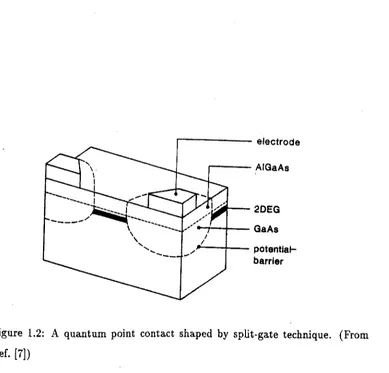
41.2 A quantum point contact shaped by split-gate technique. (From Ref.
[7]) . . . ..
6
1.3 A diagram of experimental arrangement in the Hallmeasure-ment. Sand D stand for electron source and drain. VL and VH are the longitudinal voltage drop and the Hall voltage
respec-tively. (From Ref. [3~)) 12
1.4 The Hall resistance Rx'IJ and the longitudinal resistance Rx:& of
the 2DEG in a Si/8i02 inversion layer as a function of applied
gate voltage
Vg.
(From Ref. [31]) . . . .. 132.1 Quasi-2D density of states
p(
E) as a function of energy with only the lowest 2D·subband occupied (hatched). Insert: Confinement potential perpendicular to the plane of the 2DEG. (From Ref. [39J) 18 2.2 QID density of states peE) as a function of energy with four2.3 Calculated potential profiles at 4.2 K along a line 5.6 nm from the GaAs/ AlxGal_xAs (x
=
0.26) interface for four values of gate voltage. (From Ref. [43]) . . . .. 22 2.4 Energy-orbit centre phase diagram. Different types of classicaltrajectories in a magnetic field are shown (clockwise from the left: skipping orbits on one edge, traversing trajectories (only one direction is drawn here), skipping orbits on the other edge and cyclotron orbits). The hatched region is forbidden. (From
Ref. [39]) 26
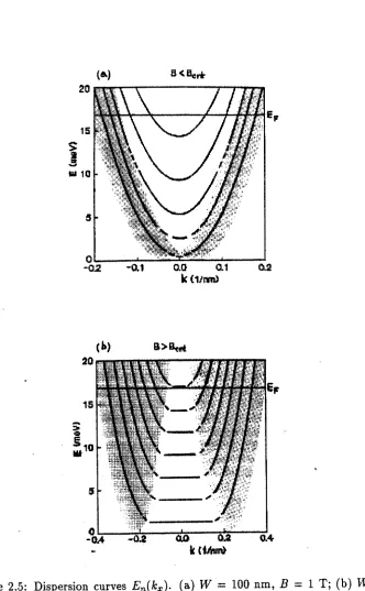
2.5 Dispersion curves En(kx). (a) W
=
100 nm, B=
1 T; (b) W=
200 nm, B=
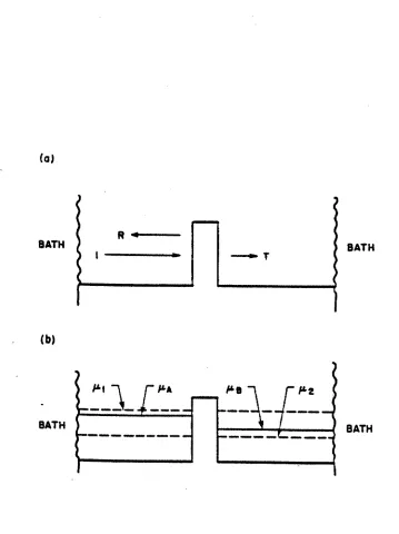
1.5 T. The shaded area is the region of classical skipping orbits and Bcrit =21ikF/eW. (From Ref. [39]). 283.1 (a) An array of obstacles connected to two incoherent reservoirs by ideal ID conductors. The obstacle array is represented by a potential barrier characterised by transmission and reflection probabilities
T
andR.
(b) The chemical potentials in the single-channel case. The chemical potentials for the source and drain are{Ll and {L2 respectively. {LA and {LB are two chemicalpoten-tials which characterise the electron densities in the two ideal
leads. (From Ref. [69]) 37
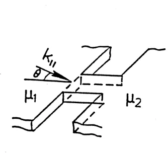
3.2 A four-lead system connected to four reservoirs via four perfect leads (unshaded). An external magnetic field is applied as rep-resented by the magnetic flux ~. (From Ref. [75]) 40 . 3.3 A configuration for calculating contact resistance. . 44
5.1 The Hall. resistance (solid curve) for a three Landau level sit-uation. The results from simple channel- counting arguments (dashed curve)' and the classical result (straight dashed line) are
also given as reference. (From Ref. [99]).: •• 63
5.3 Current density
jx(y):
(a) B =0.25 T andIjx(y)lmax
=0.3354A/m and (b) B = 1.25 T andIix(y)lmax
= 1.6968 A/m; EHPV(y):
(c)
B
=0.25 T and (d)B
=1.25 'I'; andU(y)
=p,(y)/(-e):
(e)B
=
0.25 T and (f) B=
1.25 T. The offset to the LCP in (f) is 0.458 mV. Wire width isW
=
100 nm and electron chargedensiitvy iIS ns
=
4X 10¹⁴m-2 . 695.4 Plots versus B of the two kinds of intrinsic Hall resistance, REHP
(squares) and RLCP (circles), and the longitudinal resistance (crosses) for a quantum wire of width 100 nm with the electron densities (a)
n,
=
2 x 10¹⁴m-2 and (b) ns=
4X 10¹⁴m-2• Thedashed lines in (a) and (b) are the corresponding Hall resistances
for an unconfined 2DEG. 70
5.5 Plots versus
B
of the intrinsic Hall resistances, SCREHP (squares) and non-SC REHP (dotted squares) as well as non-SC RLCP (cir-cles), and the longitudinal resistance (triangles) fora quantum wire of width 100 nm with the electron density ns =4x 10¹⁴m-2,The dashed line is the corresponding Hall resistances for an
un-confined 2DEG , . , , ..•.... , , 71
5.6 Dispersion curves for a transport BQW in a magnetic field with threesubbands occupied (top). The unit for the vertical axis is
hwc• The corresponding distributions of electron wave functions,
F(y),
(bottom). Each of them is normalised by dividing by itsmaximum absolute value across the wire. 73
5.7 Normalised current density,
I(y),
and EHP,V(y),
distributions when there is one subband occupied (top) and three sub band occupied (bottom). The system is the same as in Fig. 5.6. . . .. 74 5.8 The SC (solid line) and the non-SC (dashed line) electron wavefunctions,
tPi(y),
fora BQW with W ::::100 nm and ns=
4 x 10¹⁴m-2• There are two sttbbands occupied when B=
0.0251'(top), while there is only one subband occupied when
B
::= 1.0 T5.9 The se (solid line) and the non-Se (dashed line) changes of electron density, dey), for a BQW with W = 100 nm and n, =4x 10¹⁴ m-2• There are two subbands occupied when B =0.025 T
(top), while there is only one subband occupied when B
=
1.0 T (bottom). . . .. 77 5.10 The se (solid line) and the non-Se (dashed line) EHPs, v(y),for a BQW with
W
= 100 nm and n,=4 x 10¹⁴m-2• There aretwo subbands occupied when B = 0.025 T (top), while there is only one subband occupied when B
=
1.0 T (bottom). . . .. 78 5.11 The se (solid line) and the non-Se (dashed line) Leps,/-t(y),
for a BQW with
W
=
100 nm and ns=
4 x 10¹⁴m-2• There aretwo subbands occupied when B =0.025 T (top), while there is only one subband occupied when
B
=
1.0 T (bottom). . . .. 79 5.12 The se (solid line) and the non-Se (dashed line) currentdensi-ties,
j(y),
for a BQW with W=
100 nm and ns=
4 X10¹⁴ m-2•T.here are two subbands occupied when
B
=
0.025 T (top), while there is only one subband occupied when B=
1.0 T (bottom). . 80 5.13 The net current density associated with the case of Fig. 5.12.The solid curve with two minima is the se and non-Se results at B =0.025 T, while the solid and dashed curves with only one minimum are the se and non-Se results at B
=
1.0 T respectively. 81 5.14 The se resistances versus ns, (a); the se resistances versus W,(b); and the non-Se resistances versus W, (c). The circles, squares and crosses refer to RLCP, REHP and the longitudinal resistance in the wire. The parameters are fixed as W
=
100 nm in (a), ns=
2 x 10¹⁵m-2 in (b) and (c) as well as B=
0.5 T forall the three. 83
,
5.16 The distributions of electron wave functions versus B. Up( down)-triangle refers to the mean position of right (left )-going wave
func-tions and the cross hatch lines sloping down to the right (left )
mark the corresponding wave function spread. The width of wire
is
W
= 100 nm and the electron densities are ti; = 14.45x 10¹⁴ m-2• 865.17 The SC LCP distributions across a BQW versus B. (a) ti, =
2,0 X 10¹⁴ m-2; (b) ns
=
4.0 X 10¹⁴ m-2; (c) ns=
8.0 X10¹⁴ m-2• The LCP is represented by ~f.L(y)/~f.L
=
(f.L(y)-f.L(W/2))/(f.L( -W/2) - f.L(W/2)). All the scales and W = 100 nmare the same for (a), (b) and (c) 88
5.18 The SC RLCP (circles) , REHP (squares) and the longitudinal
resistance (crosses) versus B. Another identical BQW is placed parallel at a distance of 100 nm; it carries a current of the same
magnitude in either the same direction, (a) and (c), or in the
opposite direction, (b) and (d). The width of the BQWs is
W
=~OOnm, ti,
=
2.0 x 10¹⁴ m-2 in (a) and (b); ns=
4.0 x 10¹⁴ m-2in (c) and (d). The dashed lines are corresponding classical results. 91
6.1 Plots showing overlap of the opposite-going wave functions in
different subbands as a function of B and the corresponding R£
(crosses) and Hall resistances: REHP (squares) and RLCP
(cir-cles). Up( down triangle refers the average position of right (left
)-going wave functions and the cross hatch lines sloping down to
the right (left )~mark the corresponding wave function spread. The
width of wire is
W :;:::
100 nm and the electron densities areRs :;:::2 x 10¹⁴m-2 in (a) and (b) and ns :;:::4 x 10¹⁴ m-2 in (c),
(d), and (e). The dashed lines show the classical Hall resistances. 95
6.2 Plots showing the dependence on ns of the opposite-going wave
functions in different subbands and the corresponding Hall
resis-tances. The width of the wire and the notation is the same as in
6.3 Plots showing REHP (squares), RLCP (circles), and RL (crosses)
vs. B for ti, = 1014 m-2 x 1.0 (a), 3.0 (b), 4.5 (c), 9.5 (d),
10.8 (e), and 19.8 (f). The width of the wire and the notation is the same as in Fig. 6.1. The dashed lines show classical Hall
resistance. . 99
7.1 Hall resistance RH calculated from Eq. (7.1) when Bp = 1 T (dashed line) and 11 T (dot-and-dash line). The RH associated with LCP and the longitudinal resistance of BQW are shown by
solid line and dotted line respectively. 109
7.2 The total form factor F (solid line) with three single mode form factor F(l) (dotted line), F(2) (dashed line), and F(3)
(dot-and-dash line) for (a) Bp
=
1 T and (b) Bp=
11 T. . 110 7.3 The ten energy levels in the measurement with Bp =1 T versusB(top) and the corresponding resistance curves (bottom). In the top figure, the dots refer to propagating modes, the circles refer to evanescent modes and the solid line refers to Fermi energy in the main BQW with
W
=
100 nm and ns=
4X 10¹⁴m-2. In thebottom figure, the solid line, dashed line and dotted line refer to the Hall resistances calculated from L-B formula, LCP and the
longitudinal resistance respectively. 113
'Chapter
1
Two-Dimensional Mesoscopic
Systems
1.1
Introduction
The real world we live -in is three-dimensional (3D) and objects in it are de-scribed by three lengths: width, height and length. Usually the length scale of each dimension is many orders larger than the microscopic characteristic lengths associated with electrons, such as de Broglie wavelength, lattice constants, etc. Then, the object is macroscopically 3D and we can employ translation invari-ance in all three dimensions when we study its electronic properties. Boundaries do not have any particular effect on the results but merely tell us how far the object extends.
Obviously, it is possible to reduce anyone of these three lengths to a very
-small value so that translational invariance does not apply in the corresponding direction. The dimensionality of the object is thus reduced. At the same time,
•
further reductions oflength in other two directions will result in one-dimensional (ID) and zero-dimensional (OD) systems.
If we only decrease the lengths in theother two directions to such a size which is comparable with some ofthe microscopic electron characteristic lengths , without destroying translation invariance, many new and novel phenomena have been observed in such two-dimensional mesoscopic systems. This is an exceedingly rich field. The ability to vary different variables results in nearly limitless possibilities for creating different structures for researches and appli-cations.
In this introductory chapter, we will briefly introduce the relevant physics of 2D mesoscopic systems and the techniques for making them. We concentrate on heterostructures and the two-dimensional electron gas (2DEG), the split-gate technique, and the basic concepts of mesoscopic and ballistic systems. At the end, the quantum Hall effect (QHE) and measurement procedure will be discussed.
1.2
Heterostructures and the 2DEG
The ability to study a low-dimensional solid state system has been longed for by condensed matter physicists for decades. The attraction of this field is their potential for exhibiting macroscopic quantum size effects and the problems associated with how to observe and control the system parameters to study them.
In 1957
J.
R. Schrieffer suaested that the narrow confinement potential ofaarinveralon
layer may lead to the observation of non-classical electron transport behaviour [1]. This was demonstrated in 1966 by measuring the low temper-ature magnetotransport properties of a 2DEG In a silicon inversion layer [2]. Since then, mtensive efforts have been made in the exploration of 2DEG sys-tems.from the rapid development of industrial technology. Ultra-thin epitaxial film growth techniques have made it possible for scientists to make a multilayered thin wafer, i.e. a heterostructure, with different materials in different layers. The first quantum well [3] was successfully made in 1974.
A Nobel Prize was awarded in this field in 1985 for the discovery of the QHE [4]: the quantisation of the Hall resistance of high mobility 2DEGs in a high perpendicular magnetic field. The system used was a 8i/8i02 heterostructure.
Si and Si02 are for the semiconductor and insulator respectively. Because of
the roughness of the crystal discontinuity at the interface as well as trapped impurities in the 8i02 and Si layers, scattering of electrons is strong and limits
the mobility of electrons to '" 4 m2/Vs or less. Further researches in this
system are therefore restricted.
In1978, a technique for creating an exceptionally pure 2DEG was invented which is known as modulation doping [5]. It spatially separates the charge carriers in a conduction band from the impurity atoms which they come. The electron mobility is then improved dramatically. This method has opened a door for the researchers to study electronic transport in ultra-high mobility carrier systems.
heterointerface. Record low temperature mobility up to 103 m2
IV
s has beenreported [6J. This corresponds to electron elastic mean free path exceeding 0.1 mm. In Fig. 1.1(b), we can see the conduction electrons supplied by the donors in the AlxGal_xAs layer are confined in a very narrow potential well the the interface of GaAs and AlxGal-xAs. This confinement potential well is formed by the competition between the repulsive potential barrier due to the band offset at the interface of GaAs and AlxGat_xAs and the attractive elec-trostatic potential resulted by the positively charged donors in the AlxGal-xAs
layer.
(a) (b) energy __.,..
17nm GaAs
38nm AIQ,33Gao.67As
1.33 • 1o~8cm-3Si
t
20nm Alo.33Gaa.67Asc: .2
i
'6 s:i
4IJm GaAse
ClI
super lattice I
valence : conduction
band I band
[image:21.503.40.412.306.616.2]semi insulating GaAs substrate
Figure 1.1: Layers of a modulation doped GaAsl AlxGal-xAs heterostructure (a) and the corresponding band-bending diagram and 2DEG (b). The numbers here are typical. The band offset between GaAs and AlxGal_xAs is about 0.3 eV when x =0.33. (From Ref. (7])
I
perpen-dicular direction. This results in the formation of 2D sub bands in the well. Because the wavelength of these conduction electrons at the Fermi energy is much larger than the GaAs lattice constants, we can use the effective mass ap-proximation and treat the electrons collectively as a gas with a certain density , moving in a continuous background. (The Fermi wavenumber kF
=
(21t'ns)1/2and typically the sheet electron density isns "" 1015m-2 the Fermi wavelength
is AF = 21t'/kF rv 80 nm.) We can further just concern ourselves with the 2D behaviour of the electron gas since only the lowest subband is usually populated in typical experimental situations. Based on the above understandings, it will be sensible to model these confined conduction electrons as a 2DEG in the heterostructure when we calculate its electronic properties.
1.3
Split-gate Technique and Microstructures
One of the most important feature of a 2DEG is that we can shape it into any desired ultra-small geometry. There are two approaches, etching a pattern which results in permanent removal of parts of the 2DEG, or using a patterned gate electrode to deplete parts of the 2DEG electrostatically and reversibly. The later is known as split-gate technique [8]. By applying a negative voltage to the split-gate. the 2DEG immediately beneath the gate electrodes is depleted and the 2DEG is laterally constrained within the area between the electrodes.
A microstructure is such a patterned 2DEG.
Lithographic techniques are used in creating the gate. Because of the very high spatial resolution needed
«
10 nm), both X-ray and electron beams are employed to generate the photo-lithographic masks which are essential in producing patterned gates. Electron beam which can be focussed into spot sizes less than 1nm,--+-- potential-barrier
Figure 1.2: A quantum point contact shaped by split-gate technique. (From Ref. [7])
.
[13). Recently, microstructures have been fabricated for which the presence or absence of a single electron affects the transport properties [14, 15]. This effect is known as Coulomb blockade which is beyond the range of this thesis.
An additional gate electrode is often put on the top of a microstructure to change the sheet electron density n, under it as the electric field applied on the electrode varies. Alternatively, split-gate electrodes can be used to do the same thing. This enables us not only to study the density dependence of the electronic transport properties of a 2DEG but also to explore the limit of electronic conduction when the number of the conducting electrons is small. The sheet density of electrons under a large gate electrode depends linearly on the electrostatic gate voltage according to the formula for a parallel plate capacitor Llns
=
ELlVg/eD, where the static dielectric constant of GaAs is E=
12.8Eoand D is the distance between the gate electrode and the 2DEG.1.4
Characteristic Lengths and Ballistic Systems
The dramatic improvement in the fabrication of ultra-small conducting devices (microstructures) has greatly increased interest in the novel electron transport phenomena because of the quantum interference which occurs in such systems.
A microstructure is called mesoscopic as if it shows quantum size effects which can be measured macroscopically but de not have a macroscopic explana-tion. Mesoscopic systems occupy the area between the microscopic world which requires a quantum mechanical description and the macroscopic world where we believe classical physics are normally adequate. Many different quantum interference behaviours have been observed and predicted. There are a lot of parameters involved, such as composition, band offset, dimensions, impurities (density and distribution), etc. It is very helpful that we can use some simple quantities as the criteria for classifying mesoscopic systems according to their electronic characteristics. The most convenient and most often used are ratios of the spatial dimensions of a system to its electronic characteristic lengths.
Typical characteristic lengths associated with electronic transport prop-erties are elastic and inelastic mean free paths, the phase coherence length, the magnetic length and lattice constants. Most of them are system dependent. The elastic (inelastic) mean free path is the average distance between two elas-tic (inelaselas-tic) scatterings of an electron. The phase coherence length measures how long an electron travels without the phase memory of its wavefunction changing.
The ratios of these. lengths to the system dimensions are crucial. For exam-ple, quantum interference effects in a system, e.g. the Aharonov-Bohm effect [16] in the magnetoresistanceof a mesoscopic ring, are found to disappear ex-ponentially when the relevant space dimension becomes large compare to its phase coherence length.
A system with a size much larger than its inelastic mean free path is dif-fusive and phase random and can be treated classically. Then, random phase
'"
larger than its elastic mean free path is diffusive but quantum coherent. It is interesting to notice that an inelastic scattering is not necessarily a dephasing scattering because phase coherence has been observed in the presence of finite energy transfer [17].
Quantum coherent diffusive systems are divided into three classes. The first class shows weak localisation effects in the average conductance
[18].
This effect arises from the coherent back-scattering of diffusing electrons, which is sensitive to a weak magnetic field. The behaviour of this effect depends on dimensionality but not the system size as long as it is about or smaller than the inelastic mean free path. The second class shows reproducible conductance fluctuations in a changing magnetic field[19].
The relation of the conductance to the magnitude of an applied magnetic field is system dependent while the amplitude of the fluctuation is universal. The universality arises because the maximum sensitivity of conductance to the change of magnetic field ise2 / handis independent to the average conductance itself. This effect depends on the ratio of the inelastic mean free path to the system size. Unlike the first two classes which are defined by their low temperature properties, the third class is determined to the thermodynamic properties of quantum coherent mesoscopic system, such as the persistent current [20, 21] and orbital magnetic response
[22, 23]. The origin of this class is not clear. Theoretical prediction shows that there should be an average effect due to the constraint of fixed particle number in a mesoscopic system [24]. All these three interference effects involve diffusing electrons and have their mathematical origin in the properties of the disorder-averaged two-particle Green function. More details can be found in Ref.
[25].
wave-functions without randomness can be observed, such as the Aharonov-Bohm oscillations of the resistance in small metallic ring structures [26].
Furthermore, the phase-preserving properties of electron wavefunctions will be ensured if the dimensions of a system is smaller than both the elastic and inelastic mean free path. This kind of quantum coherent system is known as
ballistic
system. In this regime, quantum transport becomes dominant and the wave nature of the electrons becomes apparent. The motion of electrons in a ballistic system is of course coherent and the energy and momenta are quantised. The resistance is non-local and has a quantum mechanical aspect. The average velocity is not an appropriate basis for a description of the resistance.An electron waveguide [27] is a ballistic quantum wire (BQW) made of a 2DEG, which is so clean and so small that electron waves can propagate in guided modes without loss of phase coherence. The propagating modes of elec-trons are characterised by its quasi-one-dimensional (QID) geometry. Atomic precision of lithography and crystal growth is needed in fabricating a ballis-tic quantum wire demonstrating the transport characteristics of an electron waveguide.
There are obvious differences between an optical or microwave waveguide and an electron waveguide. The guided mode of electron is sensitive to an applied electric or magnetic field because it possesses a charge. Moreover, the number of electrons in a specific mode of the waveguide is limited by the Pauli principle due to the fermion feature of electrons.
1.5
Four-leadMeasurement
and the QHE
Conductance and resistance, as .well as conductivity and resistivity, are the most frequently used quantities in characterising the electronic transport properties of a system. The "ances" represent the global features of the system being studied, while the "ivities" are used torefer the local properties; Exp,er:~Jjl1e:p... talists usually use the "ances" because they measure them directly. While,
'"
the suitable quantities in describing the system because these quantities are not additive any more. For the same reason, in this thesis, we concern the "ances" rather than the "ivities".
For a steady transport system, the resistance is defined as the electrostatic voltage difference applied on the system divided by the amount of the current driven through it (or. equivalently using electrostatic voltage difference induced in the system divided by the amount of the current injected into it). The elec-trostatic voltage drop on a system comes from the electrochemical potential difference between two voltaic electron reservoirs which are connected to the system as current source and drain respectively. The electrostatic voltage dif-ference is normally different from the electrochemical potential difdif-ference when the internal resistance between the current source and drain is finite. How-ever; these two differences become one if the internal resistance between the two reservoirs is much larger than the resistance of the system. This is usually true in high accuracy resistance measurements. We assume that this is also the case in our calculations.
The primary resistance measurement uses a pair of leads connected at the two sides a system. The current flowing through and the voltage drop on the system are measured with the same pair of leads. The problem of this method is that the contact resistances at the two sides of the system becomes parts of the measured resistance of the system, so that the final results can be signifi-cantly distorted if the system resistance itself is smaller than or comparable to the contact resistance. For excluding this extra part of resistance, four-lead
measurement is introduced. Two pairs of leads are used to measure current
high precision measurement.) For the same reason, the current in the current leads is equal to the current traversing through the system. Consequently, we can use four-lead configuration to measure the electrochemical potential differ-ence applied on a system and the induced current traversing it and exclude the potential drops on the voltage contacts.
The Hall effect was discovered in metal wires in 1879 by E. H. Hall [28].
He observed "the state of stress in the conductor" in the case that "the magnet may tend to deflect the current ... ". This state of stress appears as transverse voltage (known nowadays as the Hall voltage) [29]. Generally speaking, the Hall effect is that the current in a conductor or semiconductor under a perpendicular magnetic field will induce a potential difference in the third direction which is perpendicular to both the current and the magnetic field. In an electric field E, the induced current density j has a linear relationship with it: E
=
po,j. The normal longitudinal resistivity for a homogeneous electron gas system with the charge of electron -e isPo = m" /nse2To, where m" is electron effective mass,in order to avoid the complexity caused by system geometry.
s
o
Figure 1.13: A diagram of experimental arrangement in the Hall measurement.
Sand D stand for electron source and drain. VLand VH are the longitudinal voltage drop and the Hall voltage respectively. (From Ref.
[30))
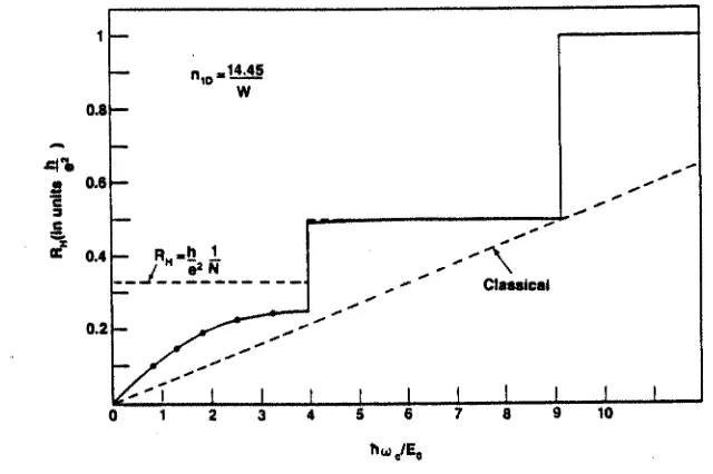
The Hall resistance normally increases smoothly when the magnitude of the applied magnetic field increases. In 1980, von Klitzing, Dorda and Pepper ob-served the integer
QHE
(IQHE) [4]. They found that the Hall resistance of the 2DEG in a Si/Si02 inversion layer was fully quantised as the unit ofhi
e2di-vided by integers at helium temperature and in a strong magnetic field of order 15 T. The accuracy of the quantisation is exceptionally high: about one tenth ppm. A typical experiment result of Hall resistance Rxy and longitudinal
resis-tance Rxx is shown in Fig. 1.4. Two years later, the fractional
QHE
(FQHE)was also observed for which the quantisation is a rational fraction ofhje2 [32].
LANDAU-LEVEL FILLING
2 4 6 8
12 20
10 10
4
Figure 1.4: The Hall resistance R:cy and the longitudinal resistance R:c:c of the
2DEG in
a.
Si/Si02 inversion layer as a function of applied gate voltage Vg.(From Ref. [31])
Chapter 2
The electrons in the 2D
microstructures
2.1
Introduction
As we already have seen in.the previous chapter, a system can be characterised by its dimensions compared with some relevant length scales. In this chapter, we are mainly concerned with the Fermi wavtength AF = 21rjkF where kF is the electron wavevector at the Fermi surface. Reduced dimensionality arises when at least one dimension of a system is comparable to AF. A system is dy-namically 2D when only one dimension is small. The motion of electrons in the corresponding direction is quantised which is known as spatial quantisation.
As a simple model, the 2DEG has proved to be very successful as a starting point to discuss the physics of real microstructures [35]. The reason is that it retains the most important feature of the electrons: that they are dynamically free to move in only two dimensions. The details left out of this simple model, which are associated with the confinement in the third direction, are not very important for studying transport properties. Of course, there are some partic-ular situations where a many-body description is necessary which we do not discuss in this thesis.
and the geometrical confinement of microstructures. Particular attention will be payed to a simple example, i.e. the quasi-one-dimensional (QID) BQW which is dynamically ID with the length shorter than the electron mean free path. The BQW will be used later as the system in which we study the IIQHE. Different ~ypes of electric confinement, as well as the Coulomb interactions between the electrons, will be briefly discussed. At the end, further confinement produced by an external perpendicular magnetic field will also be considered.
2.2
The effective mass approximation
and 2D
fea-tures of a 2DEG
It is convenient to describe some of the characteristics of quantum mechanical wavefunctions in the terms of classical mechanics. Some classical concepts, such as group velocity and mass, can be extended. To build up the relationships be-tween these quantities in the two pictures, we normally use de Broglie waves of electron to construct a quantum wave packet which behaves like a classical particle. In a lattice, Bloch waves are used instead of de Broglie waves. Cor-respondingly, some classical concepts are therefore meaningful in the quantum case. The group velocity of a wave packet v and its effective mass m* are
(2.1)
and
112 mj = --;(
-:o2-
E--),Okj2
where E(k) is the energy of a packet with momentum k. Since these results
j
=
X,y,z
(2.2)do not contain any restrictions on the construction of the wave packet, they can further be extended into general situations. In the effective mass ap-proximation, the effective mass mj in Eq. (2.2) is assumed to be constant.
band. It may be questionable whether this approximation is appropriate in the case when there are only a few atomic layers in one or more directions. As is often the case, the approximation turns out to be rather good. Nevertheless, it loses validity for monolayer structures. Approximations that take account of the discrete atomic structures are then required [38J. In this thesis, the effec-tive mass approximation will be used because it has been proven to be a good approximation to 2DEGs [35].
The one-electron Hamiltonian for a 2DEG which is dynamically free in the
x-v
plane is2
H
=
2P+
V(z)
m* (2.3)
where P =
-in"
andV(z)
is the confinement potential in thez
direction. To determine the eigenfunctions of1i,
we consider a macroscopic square of side Lin the
x-v
plane and apply periodic boundary conditions in both thex
and ydirections. Since the
1i.is
independent ofx
and y, the eigenfunctions take the plane-wave form(2.4) where r
=
(x,y)
and k=
(k:c, ky) with both k:cand ky equal to integer multiples of 211"/ L. By substituting the Eq. (2.4) into the Eq. (2.3), we find that the eigenvalue associated with '!/Yak is(2.5)
where Ea and <Pa(z) are determined by the 1DSchrodinger equation
(2.6)
and k2 = k;
+
k;. In general, the value of kmay be taken to be continuous,reflecting the macroscopic size of the 2DEG in the
x-v
plane. The index a which labels the solutions of Eq. (2.6) takes positive integer values.,We see clearly from Eq, (2.5) that the energy spectrum of the ,2DEG consists of,,2D subbands which are distinguished by the index a. Each Ea defines
/;
familiar 3D energy spectrum where there is only one continuous parabola from
E
=
0 upwards. The gaps between the sub band minima increase when the confinement potentialV(z)
is narrowed. As an example, let us consider a square well potential of widthLz
V(z)
= { :
0<
z<
L
z,otherwise.
(2.7)
Solving Eq. (2.6), <Pa(z)and Ea are
(2)1/2
(0:1I"Z)
<Pa(Z)
=
t...
sinLz
'
"(2.8)
_ 11,2
(0:11")2
Ea - -- -- •2m* L, (2.9)
When the width
Lz is
of the order of the electron Fermi wavelengthAF
=1/kF,
the Fermi energy EF N Ea=l. The effect of the energy quantisation then
becomes important and the system will have distinguishable 2D features as we will see later. On the other hand, when
Lz -
00, the 3D features of thewavefunctions and the energy spectrum are restored, asEa in Eq. (2.9) becomes quasi-continuous.
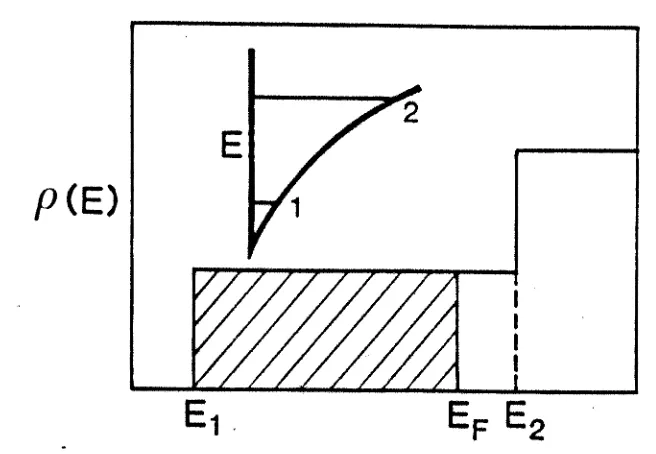
Inaddition to the energy quantisation, the density of states of the 2DEG, which is shown in Fig. 2.1, has the unique "stair-case" structure
peE)
=
2L:N
a(E)a
(L)'f
dl
=
2 ~
fJ(E - Ea)211"
IVkEa(k)1(2.10)
=
L2Nuh
L:
fJ(E - Ea)<. a
where the factor 2 is for electron spin degeneracy, fJ(E) is the unit step function and
NBsh
=
m*/1r1i2 is the density of states for a single subband perunit area. When only the lowest subband is occupied, as is usually the case for a real 2DEG, the density of states is constant which the behaviour normally associates with a strictly 2D system. As the width of the confinement at the Z directionare occupied. Therefore, the 3D character of the density of states, peE) "" E1/2,
is observable as the envelope of
p(
E) because EQ '" a2• In the limit L, _ 00,peE) will return to the familiar 3D continuous form >- E1/2.
[image:35.515.54.382.206.433.2]peE)
Figure 2.1: Quasi-2D density of states peE) as a function of energy with only the lowest 2D sub band occupied (hatched). Insert: Confinement potential per-pendicular to the plane of the 2DEG. (From Ref. [39])
2.3
A 2DEG in a BQW and Coulomb interactions
between the electrons
In aBQW, a 2DEG in the x-y plane is further dimensionally reduced to a QID-EG. A lateral confinement potential, which is normally applied by split-gate electrodes, shapes the 2DEG into a desired geometry. Assuming that this new confinement is in the y direction and is described by a potential function
U(y), the electrons are only free to move in the x direction. The electron wAvefunction tPQk in Eq,(2.4) becomes
!
( ) 1 ik:r; ( )
and the corresponding eigenvalue is
n,2k2 Ecx(kx)
==
Ea+ __
a:2m*
where i.pa(Y, z) and Ea are determined by the 2D Schrodinger equation
, - 2~*
(:;2
+
::2)
i.pa(Y, z)+
[U(y)+
V(Z)]i.pa(Z)==
Eai.pa(Y, z).(2.12)
(2.13) Since the confinement potentials U(y) and
V(z)
are independent to each other, the eigenfunction i.pa(Y, z) may take the form(2.14) and correspondingly
(2.15) where a
==
(/3,
I) with/3,
I==
1,2,···. Et3 and E'Y are normally discrete and are determined byU(y)
andV(z)
respectively. WhenU(y)
takes the form shown in Eq. (2.7), Et3 will have the same form as in Eq. (2.9) and depends on the size of the microstructure. We see that a BQW with a different size will have a different set of the electron energy levels. This phenomena is known asthe quantum size effect which has the same physical origin as the spatial
quantisation effect which we mentioned before. The eigenvalues in Eq. (2.12) can still be classified as subbands labelled by an index awith a minimum energy
Ea for each subband. Because the size of the confinement in the Y direction is normally much larger than that in the z direction, the number of the discrete levels Et3 is much bigger than the number of E'Y in any energy range. To be clear, we refer to the parts associated with Et3 as iD suhhands which are normally formed within one 2D subband (E'Y=1 in real experimental situations when Lz '" AF). In addition, the pattern of the density of states has another qualitative change associated with the further reduction of dimensionality. By using the same method lnEq. (2.10), the Q1D density of states is
as shown in Fig. 2.2. The most noticeable feature here is that there is a square root singularity at the bottom of each ID subband. It is expected that much sharper discontinuities will be associated with the ID case than with the 2DEG and that the quantum size effect will increase the number of these discontinu-ities.
P(E)
[image:37.515.53.381.231.471.2]E
1-- ...Figure 2.2: QID density of states peE) as a function of energy with four ID subbands occupied (hatched). Insert: Square well lateral confinement potential with discrete energy levels indicating the bottoms of the ID subbands. (From Ref. [39.])
Once we leave the- above over-simplified models and begin to study the electron energy spectrum in a real microstructure, calculations become more complicated. Because there
are
carriers present, the description of the poten-tial and the calculations of the energy level as well as other properties are coupled and must be solved self-consistently. Coulomb interaction between the electrons should be included in order to find out what the charge and potential di1'ltributions are. In this case, we should solve the Schrodinger and Poissonr.
sim-ple geometries can be solved exactly [36]. Variational approximations are the simplest way to obtain approximate solutions, especially for the ground state. The Fang-Howard trial function [37] was widely used. Nowadays, as full nu-merical solutions become more easily accessible, especially for the 2DEG where equations only involve one space dimension, it is less necessary to rely on vari-ational functions. A brief review of energy level calculations for 2D interacting electrons can be found in Ref. [40].
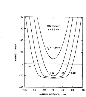
In a BQW, Schrodinger's equation must be solved in two dimensions with free electron motion only in the third dimension. This problem have been formu-lated as a set of coupled 1D equations in treating a rectangular GaAsj AlxGal-xAs wire [41]. Full numerical self-consistent calculations have been done for the electrons in silicon [42] and in GaAs [43, 44]. Normally, only the Hartree ap-proximation is used, the exchange-correlation and image effects are expected to change the results slightly [43]. The calculated confinement potential profiles [43] across a 400 nm BQW along a line 5.6 nm from the GaAsj AlxGal-xAs interface at 4.2 K are shown in Fig. (2.3). We see from this figure that when the gate voltage
Vg
=
-1.30V(ns
rv 2X 10¹⁵m-2) the effective one-electroncon-finement potential when Coulomb interaction is taken into account is somewhat like a hard wall square well. While, when
Vg
=
-1.52 V(11-s
rv 5X 10¹⁴ m-2)-> ~
400 nm SLIT
z=5.6 nm
~O~--~--~----._--~----~--~
-120 -80 ~O 0 40 80 120
[image:39.515.50.338.76.401.2]LATERAL DISTANCE (nm t
Figure 2.3: Calculated potential profiles at 4.2 K along aline 5.6 nm from the GaAsj AlxGal_xAs (x =0.26) interface for four values of gate voltage. (From Ref.
[43])
2.4
Parabolic potential with magnetic confinement
Let us consider a BQW with the 2DEG in the x-y plane and laterally confined in the y direction by a parabolic potential U(y). This is one of the few models which can be solved exactly. The Hamiltonian for motion in the plane of the 2DEG is
2
tc
=
2~*+
U(y)(p;
+
p~) 1m* 2 2=
2m*+
Q2'
(_e)wpYP2 p2 1
=
_x_+
_y_+
_m*w2y22m* 2m* 2 p
w~,ereQ :::: (-e) for electrons and the frequency wpis used to refer the strength of the lateral confinement. Because the momentum Px along the BQW commutes
with
11.,
i.e.[Px,11.]
= 0, we can diagonalise both of them simultaneously. For each eigenvalue likx of Px, the Hamiltonian has discrete energy levels En(kx)(n =0,1, ... ) with the corresponding wavefunctions taking the form
.1. 1 ik x ()
'f'n,kx = L1/2 e :r Xn,kx Y (2.18)
In. waveguide terminology, the index n labels the modes (or the channels
as in the language of electronic transport) and the dependence of the energy
En(kx) on the wave number kx is the dispersion curve of the n-th mode. The wavefunction 1/Jn,kxis the product of a transverse profile Xn,kx(y) and a longi-tudinal plane waveeikxx. Xn,kx(Y) and En(kx) are determined by the following Schrodinger equation
(2.19)
The eigenfunctions of the Eq. (2.18) are
(2.20)
with the eigenvalues
(2.21)
where
Hn
is the n-th order Hermite polynomial ande
=
(m*wp/Ii)1/2y. FromEq, (2.21), we see the familiar ID subbands again with the spacing liwp. The group velocity defined in Eq. (2.1) is equal to the velocity likx/m* obtained from the, momentum, and the effective mass is simply m* for the free 2DEG.
Next, we look at the effect of a perpendicular magnetic fieldB in
z
direction on a free 2DEG. Again only equilibrium state is concerned. In the Landau gauge A= (-
By, 0, 0), the Hamiltonian has the form11.
=
_1_(p _ qA)2+
U(y)
2m*
1
)2
P~=
2m*Cpx -
eBy+
2m*forA single spin component. Still we have
[PX111.]
=
0 and the wavefunctionsI
Eq. (2.17), we get the differential equation which is mathematically equivalent to the Eq. (2.19). This tells us that the magnetic field provides a special type of parabolic confinement (with different potential minima for electrons with different momenta). The solution Xn,kx(Y) has the same form as in Eq. (2.20) with ~
=
Ylle -lekx and En(kx)=
En=
fiwe(n+
1/2). Here, Ie=
(fileB)1/2 is the magnetic length and We =eHf m" is the cyclotron frequency. In thisparticular case, En(k
x)
does not depend on kx and we only have the Landau levels En instead of the ID subbands. Because there is only magnetic con-finement, the group velocity is zero and all the electrons are localised with an infinite effective mass.The mathematical similarity between parabolic and magnetic confinement allows us to get an exact solution for the parabolic confined BQW in a per-pendicular magnetic field B
[48].
Using the same gauge, coordinates and no-tations, we have the same solutions for Xn,k",(y) as in the Eq. (2.20) with the~ =(1+,)1/4Y
I
le-1ekxl(I+,)3/4, where, =(wplwe)2. While En(kx) has thesimilar fo~m to that in the ~q. (2.21)
(
1)
fi2k2En (kx) =lu» n
+
2
+
2M
(2.23) where w2 = w;+
w; and M = (1+ ,
)m*II.
The effective mass M here is (1+ ,)
II
times heavier and the group velocity fikx1M
is then,1
(1+ ,)
smaller than that in the free 2DEG case. The electrons no longer behave in the same way as they do when there is only electrostatic parabolic confinement, because the momentum contains an extra contribution from the magnetic vector potential. On the other. hand, unlike the case when there is only magnetic field, the electrons are no longer localised since they are delocalised from their static cyclotron motions when they are scattered by the confinement potential.
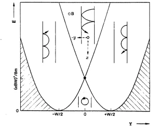
The correspondence between the electron wavefunction in a magnetic field and its classical trajectory may help us to understand more about the nature of the quantum wavefunction
[49].
It is less confusing to look .at a 2DEG in a magnetic field confined by a hard wall square well because the edges are welldefined. We will follow Ref. [39] to demonstrate this correspondence and more I,·
Let us assume the edges of a square well confined BQW are at y =±lV/2. An exact quantum mechanical solution of this problem is given in Appendix A. In the classical picture, the electron position (x,
y)
is on a circle with centre coordinates (X, Y) can be expressed in terms of its velocity v byv
x =X
+
.J!.,We
Vx
y=Y--We
(2.24)
and the electron energy E = m*v2/2 = m*w;r;/2 with the cyclotron radius
re
=
(2m*E)1/2/eB. Both the electron energy E and the shift Y of the orbit centre from the edges of the wire are constants of the motion. The shift Y is related to the electron momentum kx, the constant of motion in the quantum mechanical description, asY=
l;kx=
nkx/eB (which is identical to the average position of a free 2DEG wavefunction in the magnetic field B with the gauge we choose). On the other hand, the coordinate X along the wire changes on each reflection when the electron is scattered by one of the edges. The trajectory (x,y)
can be classified as a cyclotron orbit, a skipping orbit, or a traversin_g trajectory, depending on whether the trajectory collides with zero, one, or both of the edges of the wire. Using the conditions (Y±
W/2)=
rc,we can separate these three types of trajectories in the space (Y, E) by two parabolas (Y
±
W/2)2 =2m*E(eB)-2 as shown in Fig. 2:4.The quantum mechanical dispersion curves En(kx) can then be fitted into the above classical picture by the correspondence kx =YeB [h, We may apply the Bohr-Sommerfeld quantisation rule to the classical motion in the y direction,
s.e.
k
f
pydy+ ;
=
21m, n=
1,2" .. (2.25) to find out the dispersion curve with sufficient accuracy for our purpose here. The phase shift; is the sum of the phase shift at the two turning points of the projected motion along the y direction. The phase shift is 1!' when "»changes sign by the reflection at the edge and -1!' /2 when Vy changes sign continuously.Consequently, ; is -1!' /2 - 1!'/2
=
1!' (mod 21!') for a cyclotron, 1!' - 1!'/2=
1!'/2 for a skipping orbit, and 1!'+
1!'=
0 (mod 21!')for a traversing trajectory. By",:
y-Figure 2.4: Energy-orbit centre phase diagram. Different types of classical trajectories in a magnetic field are shown (clockwise from the left: skipping orbits on one edge, traversing trajectories (only one direction is drawn here), skipping orbits on the other edge and cyclotron orbits). The hatched region is forbidden. (From Ref. [39])
using Eq. (2.24), py
=
m*vy=
eB(x - X) and Eq. (2.25) takes the formB
j(x -
Y)dy= ~ (
n -
2:) .
(2.26) This quantisation condition has a geometrical interpretation: n -,121r
flux quanta hie are contained in the area bounded by the wire edges and a cy-clotron circle centred at Y with radius (2m·E)1/2IeB. The electron energyE
=
m·v2/2
will be calculated with the aid of Eqs. (2.24) and (2.26). Thedispersion curve for En.(kx) can then be carried out straight forwardly for each
integer n and momentum Y by using the relation kx
=
Y eBIn.
The results are shown in Fig. 2.5. The regions occupied by the classical skipping orbits~;"
[image:43.515.51.366.123.386.2]trajecto-ries at larger E. From Fig. 2.5, we can easily see the correspondences between these classical trajectories and the parts on the quantum dispersion curves. The cyclotron orbits correspond to the Landau levels which are the flat portions of the dispersion curve at En = (n - 1/2)11;.;;c. The group velocity is zero for a Landau level, which is identified with a circular orbit. The traversing trajec-tories, which interact with both the opposite edges and have a nonzero group velocity, correspond to the lD subbands where both the electrostatic confine-ment and the magnetic field are present. The skipping orbits correspond to the edge states [50], which interact with a single edge only. The two sets of the edge states (one for each edge) are separated in the (k, E) space. Edge states at opposite boundaries move in opposite directions, which is the same as for the skipping orbits. Finally, the critical field Bcrit
=
21ikF/eW in Fig. 2.5 iss
J
0..0 0.1 0.2
It;(1,Ma)
[image:45.515.60.392.81.618.2]B>But
Chapter
3
Electronic transport:
Landauer-Buttiker
formulae
3.1
Introduction
Transport in a system is a phenomenon associated with a non-equilibrium state. A system- is in a non-equilibrium state if there are any kind of "potential" differences between any two spatial points in it so that a "flow" is built up from a source to a drain which are associated with the high and low "potentials" respectively. The dependence of the amount of the "flow" on the "potential" difference is generally nonlinear. Because of the difficulty of dealing with the nonlinearity there is no unified theoretical approach to non-equilibrium systems. Only the so-called near-equilibrium systems have been systematically studied in a unified picture
[51].
In a near-equilibrium system, the difference between the "potential" /-Ls at the source and the "potential" /-Ld at the drain is so small that the "flow" can be treated as a linear response of it. We would like to use 2(/-Ls - /-Ld)/(/-Ls+
/-Ld) 0 as the criterion of near-equilibrium instead of the conventional (/-La - /-Ld) 0, since we believe any system in which /-Ls>
/-Ld =0 is far. from equilibrium. In fact, a system is in a near-equilibrium state only if the amount of net current is much smaller than both of the currents from source and drain.corre-sponding to different kinds of potential differences. Current, i.e. the charge flow, is induced by the electrochemical potential differences in a system. The ratio of the potential difference to the current is defined as the resistance be-tween the two corresponding points in the system as in the well known Ohm's law. While the ratio of the change of the potential difference to the change of the current is known as the differential resistance. It is understandable that these two kinds of resistances are generally not equal to each other and that both of their magnitudes depend not only on the average chemical potential in a system but also on the potential difference. If a system is in the near-equilibrium regime, the linearity of electronic transport will merge these two resistances into one constant which depends only on the chemical potential of the system and can be used to characterise the system response. This is the resistance we are going to study in 2DEG microstructures in this thesis.
Resistance comes from the disturbance produced by different kinds of "im-purities" on the directed motion of the charge carriers which are the electrons in solid state materials. We can see this from a simple classical example. In a 2D infinite space without any impurities the current density j will approach infinity because the infinite velocity of free electrons which are accelerated by a constant electric field
E.
Hence, the resistivity p defined byE
=
pj must approach zero. On the other hand, the electron velocity and the correspond-ing current density cannot be arbitrarily large as long as there is an impurity distribution in the system because there is always some momentum loss asso-ciated with scattering. It is very obvious that a classical resistance problem is very similar to a classical diffusion problem. The concepts of the mean free path I and the relaxation time r have been borrowed from there. They refer to the average distance and time respectively between two electron-impurity scattering events. The resistivity may be found easily [52] as p = m*/ne2r,where m" is the electron mass and n is the density of electrons. More detail calculations can be performed by using a distribution function f(r, p,
t)
which expresses the fraction of states occupied and its time dependence, where r and,"
density of a fluid in 6-dimensional (r,
p)
space, the equation of continuity has the form(3.1) where V is a 6-dimensional velocity composed of the electron velocity v =
O~/Ot
and the force on electrons F =Op/Ot.
Because rand p are conjugatecoordinates and the Hamiltonian equations held for them, we will have V'.V
=
0 and(3.2)
by the Liouville's theorem [53]. In the presence of impurities, electrons being scattered in the p-space can not be fully described by the force Fand a sup-plement term to include the effect of scatterings is needed. Using the relation
p=tik, we have the Boltzmann equation in the form
df
=
Of
+
v. V'rf+
Ok .
V'kf=
(df)
dt
at
at
dt scatteringswhere the right-hand side is the time rate of change due to the scattering by (3.3)
impurities. To solve Eq. (3.3), a relaxation time approximation is often used [55], which is
(dt)
scatterings= -
f ~ fo (3.4)where fo is the equilibrium distribution function. For a simple homogeneous system at low temperatures with randomly located impurities: f
=
f(k) for the steady state. Then we have the resistivity in the same form, p =m*/ne2r( kF),for a free EG [36], where r(kF) is the relaxation time for the electron at the Fermi level. The Boltzmann equation is derived from the classical point of view [54]. In principle, the Boltzmann equation may only be used when wave packets can be constructed. Nevertheless, it sometimes produces similar answers as a quantum calculation even when this criterion is not satisfied.
Electronic transport in microstructures is a kind of quantum transport be-cause the Fermi wavelength is of the order of the microstructure dimensions. Furthermore, the time for electrons traversing the system is equal or less than
",."