N A N O E X P R E S S
Open Access
Efficient TiO
2
Surface Treatment Using
Cs
2
CO
3
for Solution-Processed Planar-Type
Sb
2
S
3
Solar Cells
Wook Hyun Kim
†, Sungho Woo
*†, Kang-Pil Kim, Soo-Min Kwon and Dae-Hwan Kim
Abstract
We report a highly effective surface treatment method for planar-type Sb2S3 solar cells by employing a
Cs2CO3-modified compact TiO2 (c-TiO2) electron transport layer. It is found that surface treatment using a
Cs2CO3 solution can shift the work function of c-TiO2 upward and reduce its surface roughness. As a
result, compared with the power conversion efficiency of untreated solar cells, that of the treated solar cells with a glass/FTO/c-TiO2(/Cs2CO3)/Sb2S3/P3HT/Au structure significantly improved from 2.83 to 3.97%.
This study demonstrates that the introduction of Cs2CO3 on a c-TiO2 layer is a simple and efficient way
to adjust the work function of the electron transport layer and fabricate high-performance planar-type Sb2S3 solar cells.
Keywords: Planar-type Sb2S3 solar cell, Electron transport layer, Surface treatment, Solution process, Cs2CO3
Background
Recently, many inorganic metal chalcogenides based on earth-abundant elements such as copper zinc tin selen-ide (CZTS), lead sulfselen-ide (PbS), copper (I) sulfselen-ide (Cu2S),
tin sulfide (SnS), and antimony sulfide (Sb2S3) have been
investigated as absorber materials in low-cost thin film
solar cells in order to replace the mainstream
solution-processible absorbers such as copper indium gallium selenide (CIGS) and cadmium telluride (CdTe)
[1]. However, the use of CZTS and PbS in the industry
has severe drawbacks, because CZTS uses the toxic and
harmful hydrazine (N2H4) and requires the complex
control of multi-compound [2] and PbS contains Pb,
which is also toxic and hazardous. Other potential mate-rials such as Cu2S and SnS have relatively low
efficien-cies compared to those of CIGS and CdTe. Sb2S3,
however, has attracted attention as a candidate material due to its suitable band gap (~ 1.65 eV) and high absorp-tion coefficient (> 105cm−1) for efficient light absorption, high dielectric constant for exciton dissociation, and
good band alignment with various hole transport layers (HTLs) for efficient charge carrier transfer, in addition to its cost effectiveness, low toxicity, and excellent air stability [3–6].
There are two types of Sb2S3solar cells based on the
device structures: sensitized solar cell or planar-type
solar cell. Sensitized solar cells originated from
dye-sensitized solar cells (DSSCs) and have a F-doped
tin oxide (FTO)/compact TiO2 (c-TiO2)/mesoporous
TiO2 (m-TiO2)/Sb2S3/HTL/Au structure, while
planar-type solar cells have a FTO/c-TiO2/Sb2S3/HTL/
Au structure [7].
In terms of device efficiency, sensitized Sb2S3 solar
cells have a higher value than planar types due to their enhanced light-absorbing interfacial area owing to the
m-TiO2 structure. The factor that decides the
perform-ance of sensitized solar cells is their interface quality in-side the device where charge carrier separation and transfer occur. Therefore, significant effort has been de-voted to the optimization of the interfacial properties, including those of the m-TiO2/Sb2S3 interface, Sb2S3/
HTL interface, and HTL material itself [8]. Various kinds of HTL materials, such as 2,2′,7,7′ -tetrakis[N,N-di(4--methoxyphenyl)amine]-9,9′-spirobifluorene
* Correspondence:[email protected]
†Wook Hyun Kim and Sungho Woo contributed equally to this work.
Convergence Research Center for Solar Energy, Daegu Gyeongbuk Institute of Science and Technology (DGIST), Daegu 42988, Republic of Korea
(Spiro-OMeTAD) [9]; CuSCN, an inorganic p-type ma-terial [10]; poly(3-hexylthiophene) (P3HT), a conducting polymer [11]; and poly(2,6-(4,4-bis-(2-ethylhexyl)-4H-cy-clopenta [2,1-b,3,4-b′
]dithiophene)-alt-4,7(2,1,3-ben-zothiadiazole)) (PCPDTBT), a newly developed
conjugated polymer [12], have been applied to adjust the Sb2S3/HTL interface and hole transport properties
lead-ing to a high fill factor (FF) and increased short-circuit current density (JSC).
Several studies that focus on the improvement of the m-TiO2/Sb2S3 interface properties have been also
reported. Tsujimoto et al. modified the m-TiO2
sur-face using Mg2+, Ba2+, and Al3+, which effectively in-crease the power conversion efficiency (PCE) of all inorganic Sb2S3 solar cells that have the FTO/c-TiO2/
m-TiO2/Sb2S3/CuSCN/Au structure [13]. Lan et al.
used Li-doped m-TiO2 to enhance the electron
trans-port properties and change the Fermi energy level
[14]. Fukumoto et al. reported the surface treatment
of the Sb2S3/HTL interface using 1-decylphosphonic
acid (DPA), which can be attached to both an
uncov-ered m-TiO2 surface and Sb2S3 surface to reduce
re-combination and increase the open-circuit voltage (VOC) and FF [15].
In planar-type solar cells, in contrast to sensitized ones, charge carrier transport depends on the carrier mobility and diffusion length within the Sb2S3 layer,
which are strongly correlated with the morphology, grain size, and crystallinity of the layer. Hence, most research on planar-type solar cells has been focused on improving the Sb2S3 thin film quality to achieve a
large grain size and a high crystallinity by using vari-ous deposition techniques. For example, conventional
chemical bath deposition (CBD) [16], thermal
evapor-ation (TE) [17], rapid thermal evaporation (RTE) [18,
19], atomic layer deposition (ALD) [20], and
nanopar-ticle ink coating [21] have been applied to fabricate
Sb2S3 thin films. Recently, Wang et al. reported a fast
chemical approach (FCA) that can be used to gener-ate very large grain sizes via a one-step spin-coating process and subsequent annealing process using a butyldithiocarbamic acid (BDCA)-based metal-organic
precursor solution [22]. Many types of metal oxides
or hydroxides can be dissolved in BDCA, which is relatively nontoxic, inexpensive, and thermally degrad-able, and can be easily synthesized via the reaction of 1-butylamine (CH3(CH2)3NH2) and carbon disulfide
(CS2) [23].
Although the sensitized solar cells have a higher PCE (3–7.5%) than planar-type ones (2.5–5.8%), their device structure and fabrication process are complicated. More-over, they contain a high degree of interface defects. A planar-type Sb2S3 device would have more potential for
use in industrial-scale solar cells with a high efficiency
and low cost, because it is conceptually simpler and eas-ier to scale up and it is highly reproducible [24,25].
Here, we report the surface treatment of a c-TiO2layer
using Cs2CO3 solution to enhance the performance of
planar-type Sb2S3solar cells. The Sb2S3layer was
depos-ited via a simple FCA spin-coating process to realize a large grain size, which was previously reported by Wang et al.
Cs2CO3 has been widely studied for application in
organic photovoltaics (OPV) [26–28], organic
light-emitting devices (OLEDs) [29], and perovskite
solar cells (PSCs) [30, 31] to improve electron trans-port due to its low-work function property. Although Cs2CO3 is usually decomposed at 550–600 °C, Liao et
al. reported that Cs2CO3 can be decomposed into
low-work function cesium oxide via a
low-temperature (150–170 °C) thermal annealing
process [26]. However, to the best of our knowledge,
there is no study on the application of Cs2CO3 to
Sb2S3solar cells.
Surface treatment using Cs2CO3 can not only
re-duce the energy barrier by changing the work
func-tion of c-TiO2, but also reduce the series resistance
of the device by reducing the surface roughness of
c-TiO2. The treatment resulted in improved device
parameters such as the VOC, JSC, and FF, and the
PCE increased from 2.83 to 3.97%. We believe that
this surface treatment of c-TiO2 using Cs2CO3
solu-tion can provide a simple and effective way of im-proving device performance in planar-type inorganic metal chalcogenide solar cells.
Methods/Experimental
Materials Used and Synthesis of Sb Complex
Antimony (III) oxide (Sb2O3, 99.99%), CS2 (> 99.9%),
n-butylamine (CH3(CH2)3NH2, n-BA, 99.5%), cesium
carbonate (Cs2CO3, 99.9%), 2-methoxyethanol
(CH3OCH2CH2OH, 99.8%), titanium (IV) isopropoxide
(Ti(OCH(CH3)2)4, TTIP, 97%), poly(3-hexylthiophene)
(P3HT, Mw 50–70K, regioregularity 91–94%, Rieke
Metals), 1,2-dichlorobenzene (o-DCB, 99%), and ethanol
(CH3CH2OH, anhydrous) were purchased from
Sigma-Aldrich Co. and were used as received without further purification.
The Sb complex was synthesized according to a re-ported method [22]. Sb2O3(1.0 mmol) was mixed with a
solution of ethanol (2.0 mL) and CS2(1.5 mL) with
mag-netic stirring at room temperature. Then, n-butylamine (2.0 mL) was added to the solution slowly under contin-ued stirring for at least 30 min to obtain a homogenous
solution of antimony butyldithiocarbamates (Sb(S2CNH
C4H9)3). Afterwards, 2 mL of this solution was diluted
Device Fabrication
The planar-type Sb2S3 solar cells in this study have a
typical structure of FTO/c-TiO2/Sb2S3/P3HT/Au, where
P3HT is employed as the HTL. The c-TiO2layer was
de-posited onto a cleaned FTO surface by spin-coating a mixed solution of 2 mL TTIP, 60 mL ethanol, 0.225 mL distilled water, and 0.03 mL HNO3at 3000 rpm for 30 s,
followed by annealing at 500 °C for 60 min in air. For surface modification using Cs2CO3, Cs2CO3
dis-solved in a CH3OCH2CH2OH solution with certain
con-centrations (1, 3, 5, and 10 mg/mL) was spin-coated on a
10-min UV-ozone treated c-TiO2 layer at 6000 rpm for
45 s. The films were then heat-treated at 150 °C for 10 min before the Sb2S3layer was spin-coated.
For the Sb2S3thin films, the Sb complex solution was
spin-coated at a speed of 6000 rpm for 30 s, after which the films were annealed on a N2-purged hot plate at 200
°C for 1 min and 350 °C for 2 min.
P3HT solution (10 mg in 1 mL o-DCB) was
spin-coated on the Sb2S3/c-TiO2/FTO substrate at a
speed of 3000 rpm for 60 s, which was then heated on a hot plate at 100 °C for 30 min in air. Finally, the Au counter electrode was deposited using a thermal evapor-ator under a pressure of 5.0 × 10⁻⁶Torr. Each device had an active area of 0.16 cm2.
Measurement and Analysis
The surface and cross-sections of the Sb2S3 thin films
were characterized using field-emission scanning electron
microscopy (FE-SEM, S-4800, Hitachi). The surface morphology was studied using atomic force microscopy (AFM, Park NX10, Park Systems). The optical properties
of c-TiO2were determined using a UV-Vis (Lambda 750,
Perkin Elmer). The current density–voltage (J–V) charac-teristics were determined using a specialized solar cell measurement system equipped with an electrometer (model 2400, Keithley) and solar simulator (91192, New-port) with a 1-kW Xenon arc lamp (Oriel). The light
in-tensity was adjusted to one sun (100 mW/cm2) under AM
1.5G solar irradiation conditions using a radiant power en-ergy meter (model 70260, Oriel). The series resistance (RS) and shunt resistance (RSH) were calculated from the
slope of the corresponding J–Vcurves beyond VOC and
JSC, respectively. The external quantum efficiency (EQE)
was measured by a QuantX-300 quantum efficiency meas-urement system (Newport) equipped with a 100 W Xenon
lamp. The structural information of FTO/c-TiO2(/
Cs2CO3) sample was characterized by multi-purpose
X-ray diffraction (XRD) system (Empyrean, PANalytical) withθ-2θmode at a scan rate of 0.05°/sec. The electronic state and energy level were analyzed using X-ray photo-electron spectroscopy (XPS) and ultraviolet photophoto-electron spectroscopy (UPS) in an ultrahigh vacuum environment (ESCALAB 250Xi, Thermo Scientific). UPS and XPS spec-tra were obtained by using the He I line (hν= 21.2 eV) and the Al Kα radiation source (hν= 1486.6 eV), respectively. The XPS depth profiling was obtained using Ar+-cluster ion gun and etch rate of 1 Å/sec.
[image:3.595.56.539.445.713.2]Results and Discussion
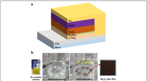
Figure1a shows a schematic of the device structure. The
bottom layer is composed of c-TiO2 layers on a glass/
FTO substrate acting as electron transporting. Light is absorbed by the Sb2S3layer, while holes are transported
by the P3HT HTL and collected at the Au counter electrode.
The Sb2S3absorbing layer was deposited via the FCA
using the Sb complex precursor to realize very large grain sizes. The precursor was thermally decomposed to the amorphous state at 200 °C for 1 min and crystalline
state at 350 °C for 2 min (Fig. 1b). The SEM image
shown in Fig.2indicates a very large grain size, which is almost the same as the Sb2S3thin film morphology
re-ported by Wang et al. [22].
The efficiency of the planar-type Sb2S3solar cell was
improved via surface treatment with Cs2CO3 of the
c-TiO2layer.
The device properties based on the concentration of
Cs2CO3 solution were performed to determine the
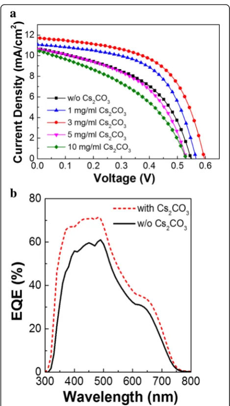
optimum Cs2CO3 concentration. Figure 3a and Table 1
show theJ–Vcharacteristics for the devices using different
concentrations of Cs2CO3solution under AM 1.5G
illu-mination (100 mW/cm2). When the concentration is too
low (1 mg/mL), there is a problem in whole coverage of the c-TiO2surface with Cs2CO3. However, if it is too high
(5 and 10 mg/mL), it acts as a dielectric material, resulting in an increase in the series resistance and decrease in the device efficiency. The optimum concentration of Cs2CO3
was found to be 3 mg/mL. (Hereafter,“with Cs2CO3
treat-ment” means treatment using 3 mg/mL concentration of
Cs2CO3unless otherwise noted.)
As a result, the device had a PCE of 2.83%,VOC of
0.549 V, JSC of 10.71 mA/cm2, and FF of 48.14% before
the treatment. However, after the treatment with 3 mg/ mL solution, all these parameters increased significantly, i.e., to aVOCof 0.596 V,JSC of 11.71 mA/cm2, and FF of
56.89%, leading to a PCE of 3.97%. This treatment re-sulted in a ~ 40% improvement in the PCE. The higher
EQE over full spectrum range as shown in Fig.3b
indi-cates that the light is more efficiently converted into current leading to increase in JSCby this Cs2CO3
treat-ment. From the EQE spectra, we can also see that the onset of EQE at 750 nm corresponds well to a band gap
[image:4.595.56.541.361.713.2]of 1.65 eV for Sb2S3 layer and a decrease in EQE from
500 to 650 nm is attributed to the absorption of P3HT HTL layer.
We measured the XRD patterns of the c-TiO2on FTO
glass substrates with and without Cs2CO3 treatment to
investigate whether Cs2CO3 has effects on the
crystallization of the c-TiO2layer and/or the formation
of new secondary phase by diffused Cs-related species.
There was no change in the XRD peak after Cs2CO3
treatment as shown in Fig. 4. This indicates that the
Cs2CO3 treatment has little effect on the crystal
struc-ture of c-TiO2 and also does not create a new phase.
Furthermore, there was no evidence of a decomposed Cs-related phase (cesium oxide, cesium suboxide, or Cs
element) after thermal treatment of Cs2CO3, which
means that the thickness of the Cs2CO3is very thin. As
shown in Fig.5d, the thickness of Cs-related species was about 2~3 nm, which was determined by XPS depth pro-file analysis for the sample of FTO/c-TiO2/Cs2CO3 (3
mg/mL). The measured thickness of Cs2CO3(2~3 nm) is
in good agreement with the AFM analysis, which shows
improved surface roughness through Cs2CO3 treatment
from 9.89 to 8.03 nm (see Fig.6a).
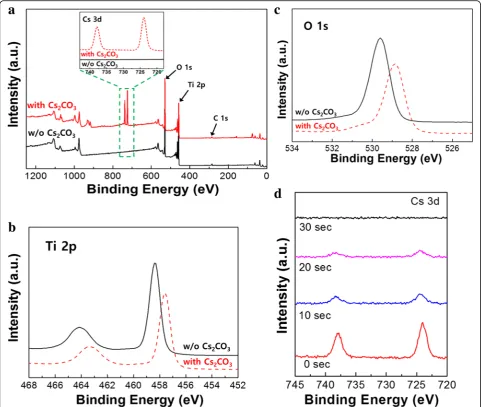
We studied the surface state of the c-TiO2layer using
XPS measurements. The XPS spectra in Fig.5show that
both the survey scan and Cs 3d peak scan clearly
indi-cate the existence of Cs on the c-TiO2 surface. The Ti
2p and O 1 s peaks were shifted to lower binding
ener-gies owing to the Cs2CO3 treatment, which indicates
that the Cs2CO3treatment affected the electronic
struc-ture of the c-TiO2 layer. The appearance of a slight
shoulder at ~ 531 eV in the O 1 s spectrum could be at-tributed to the cesium oxide generated from Cs2CO3
de-composition via annealing at 150 °C, which has a low work function [26].
[image:5.595.56.291.84.498.2]Fig. 3aCurrent density–voltage (J–V) characteristics andbEQE spectra of planar-type Sb2S3solar cells with and without Cs2CO3treatment of c-TiO2
Table 1Summary of device performances according to different Cs2CO3concentrations under AM 1.5G condition
Devices VOC (V)
FF (%) J
SC(mA/
cm2) PCE(%) R(ΩScm2) R(ΩSHcm2)
Without Cs2CO3 0.549 48.14 10.71 2.83 11.14 178.56
With 1 mg/mL Cs2CO3
0.567 56.82 11.07 3.56 9.42 451.2
With 3 mg/mL Cs2CO3
0.596 56.89 11.71 3.97 8.82 454.08
With 5 mg/mL Cs2CO3
0.532 47.99 10.66 2.72 10.66 207.36
With 10 mg/mL Cs2CO3
0.531 40.78 10.50 2.27 15.17 125.76
[image:5.595.303.539.86.265.2] [image:5.595.56.290.603.732.2]The AFM images in Fig. 6a reveal a difference in
the surface morphology of the c-TiO2 layer before
and after Cs2CO3 treatment. The surface became
smoother and the root mean square roughness (Rg) decreased from 9.89 to 8.03 nm after treatment. This smooth surface was useful for increasing the physical
contact between the c-TiO2(/Cs2CO3) layer and the
Sb2S3 layer, leading to a decrease in the RS value
from 11.14Ω cm2 (without Cs2CO3) to 8.82Ω cm2
(with Cs2CO3) (see Table 1). The decreased RS may
have contributed to increasing the FF from 48.14 to 56.89% [5].
The UV-Vis transmittance spectra of the c-TiO2films
with and without Cs2CO3are shown in Fig. 6b. The
fig-ure shows that there is little change in the optical trans-mittance between wavelengths of 300 and 800 nm,
which confirms that Cs2CO3treatment has a negligible
effect on the intensity of light reaching the Sb2S3layer.
UPS was used to determine the change in the work function of the c-TiO2 layer before and after Cs2CO3
treatment to investigate the effect of Cs2CO3 on VOC.
The results are shown in Fig. 7a. The work function of
c-TiO2 decreases by 0.3 eV after Cs2CO3 treatment.
Cs2CO3is widely used as an efficient electron transport
material in many optoelectronic devices through thermal evaporation or solution process. However, the accurate analysis of electron transport mechanism and the type of decomposed Cs-related species that are responsible for electron transport property are still uncertain
and controversial. Among previous reports on
solution-processed Cs2CO3, Liao et al. showed that
Cs2CO3 can be decomposed into low work function,
[image:6.595.57.539.88.495.2]doped semiconductor in the form of Cs2O doped with
Cs2O2 after thermal annealing at 150 °C by using XPS
analysis [26]. This form of doped cesium oxide can act as an n-type semiconductor with intrinsically low work function, which might contribute to work function re-duction of c-TiO2in our system. In addition, there was
no change in the absorption onset as shown in Fig. 6b,
indicating little change in the optical bandgap of the c-TiO2after the treatment.
The energy band diagram in Fig. 7b shows that the
conduction band energy level of c-TiO2 shifted
to-ward a lower energy by 0.3 eV. This shift leads to not
only an improved VOC due to an increase in the
built-in potential (VBI) inside the devices, but also an
increased JSC due to the alignment of the energy level
between c-TiO2 and Sb2S3 to reduce the charge
trans-port barrier at the interface. The proposed operating principle is illustrated in Fig. 7c. At open-circuit
con-dition, the shifted conduction band of the c-TiO2
layer by Cs2CO3 treatment leads to the increased VBI,
which contributes to the improved VOC. At the same
time, the increased VBI results in the larger energy
band bending of the Sb2S3 layer under short-circuit
conditions, and thus the photogenerated electrons can
move quickly toward the c-TiO2 layer. This fast
elec-tron transport is attributed to cause the enhanced JSC
and FF. Thus, the Cs2CO3 treatment on c-TiO2 layer
could increase both VOC and JSC simultaneously,
lead-ing to the enhanced PCE. Hence, Cs2CO3 is a
prom-ising material for c-TiO2 surface modification as it
enhances device performance by changing the work
function and improving the electron transport
properties.
Conclusions
Cs2CO3 was found to be an effective surface modifier
to enhance the charge transport ability of the c-TiO2
electron transport layer (ETL) for planar-type Sb2S3
solar cells. The UPS data show that Cs2CO3
treat-ment can shift the work function of c-TiO2 upward,
possibly increasing the built-in potential of the device and reducing the energy barrier for charge transport.
The c-TiO2 surface became smoother after Cs2CO3
treatment, resulting in increased physical contact with the
[image:7.595.57.539.87.415.2]Sb2S3 absorber. The solar cell performance was
signifi-cantly improved in all parameters simultaneously includ-ingVOC, JSC, and FF. This resulted in an increase in the
PCE from 2.83 to 3.97%, almost a 40% increase. This study shows that surface treatment using inorganic compounds such as Cs2CO3will play an important role in the
devel-opment of highly efficient planar-type Sb2S3solar cells.
Abbreviations
AFM:Atomic force microscopy; c-TiO2: Compact TiO2; EQE: External quantum efficiency; ETLs: Electron transport layers; FCA: Fast chemical approach; FF: Fill factor; FTO: Fluorine-doped tin oxide; HTLs: Hole transport layers;JSC: Short-circuit current density;J–V: Current density–voltage; m-TiO2: Mesoporous TiO2; P3HT: Poly(3-hexylthiophene); PCE: Power conversion efficiency;
RS: Series resistance;RSH: Shunt resistance; SEM: Scanning electron microscopy; UPS: Ultraviolet photoelectron spectroscopy; UV-Vis: Ultraviolet– visible spectrometer;VBI: Built-in potential;VOC: Open-circuit voltage; XPS: X-ray photoelectron spectroscopy; XRD: X-X-ray diffraction
Acknowledgements
This work was supported by the DGIST R&D Program of the Ministry of Science and ICT of Korea (18-ET-01).
Availability of Data and Materials All data are available without restriction.
Authors’Contributions
WHK and SW designed the experiments. WHK carried out the experiments. SW prepared the manuscript. WHK and SW performed the main data analysis. KPK, SMK, and DHK participated in the discussion and analysis of the data. All authors read and approved the final manuscript.
Competing Interests
The authors declare that they have no competing interests.
Publisher’s Note
Springer Nature remains neutral with regard to jurisdictional claims in published maps and institutional affiliations.
[image:8.595.58.537.89.483.2]Received: 12 October 2018 Accepted: 6 January 2019
References
1. Azimi H, Hou Y, Brabec CJ (2014) Towards low-cost, environmentally friendly printed chalcopyrite and kesterite solar cells. Energy Environ Sci 7:1829–1849
2. Todorov TK, Tang J, Bag S, Gunawan O, Gokmen T, Zhu Y et al (2013) Beyond 11% efficiency: characteristics of state of the art Cu2ZnSn(S,Se)4 solar cells. Adv Energy Mater 3:34–38
3. Maiti N, Im SH, Lim C-S, Seok SI (2012) A chemical precursor for depositing Sb2S3onto mesoporous TiO2layers in nonaqueous media and its application to solar cells. Dalton Trans 41:11569–11572
4. Kamruzzaman M, Chaoping L, Yishu F, Farid Ul Islam AKM, Zapien JA (2016) Atmospheric annealing effect on TiO2/Sb2S3/P3HT heterojunction hybrid solar cell performance. RSC Adv 6:99282–99290
5. Lei H, Yang G, Guo Y, Xiong L, Qin P, Dai X et al (2016) Efficient planar Sb2S3 solar cells using a low-temperature solution-processed tin oxide electron conductor. Phys Chem Chem Phys 18:16436–16443
6. Choi YC, Lee DU, Noh JH, Kim EK, Seok SI (2014) Highly improved Sb2S3 sensitized-inorganic–organic heterojunction solar cells and quantification of traps by deep-level transient spectroscopy. Adv Funct Mater 24:3587–3592 7. Kondrotas R, Chen C, Tang J (2018) Sb2S3solar cells. Joule 2:857–878 8. O’Mahony FTF, Lutz T, Guijarro N, Gómez R, Haque SA (2012) Electron and
hole transfer at metal oxide/Sb2S3/spiro-OMeTAD heterojunctions. Energy Environ Sci 5:9760–9764
9. Moon S-J, Itzhaik Y, Yum J-H, Zakeeruddin SM, Hodes G, Grätzel M (2010) Sb2S3-based mesoscopic solar cell using an organic hole conductor. J Phys Chem Lett 1:1524–1527
10. Boix PP, Larramona G, Jacob A, Delatouche B, Mora-Seró I, Bisquert J (2012) Hole transport and recombination in all-solid Sb2S3-sensitized TiO2solar cells using CuSCN as hole transporter. J Phys Chem C 116:1579–1587 11. Chang JA, Rhee JH, Im SH, Lee YH, Kim HJ, Seok SI et al (2010)
High-performance nanostructured inorganic−organic heterojunction solar cells. Nano Lett 10:2609–2612
12. Im SH, Lim CS, Chang JA, Lee YH, Maiti N, Kim HJ et al (2011) Toward interaction of sensitizer and functional moieties in hole-transporting materials for efficient semiconductor-sensitized solar cells. Nano Lett 11: 4789–4793
13. Tsujimoto K, Nguyen D-C, Ito S, Nishino H, Matsuyoshi H, Konno A et al (2012) TiO2surface treatment effects by Mg2+, Ba2+, and Al3+on Sb2S3 extremely thin absorber solar cells. J Phys Chem C 116:13465–13471 14. Lan C, Luo J, Lan H, Fan B, Peng H, Zhao J et al (2018) Enhanced charge
extraction of Li-doped TiO2for efficient thermal-evaporated Sb2S3thin film solar cells. Materials 11:355
15. Fukumoto T, Moehl T, Niwa Y, Nazeeruddin Md K, Grätzel M, Etgar L (2013) Effect of interfacial engineering in solid-state nanostructured Sb2S3 heterojunction solar cells. Adv Energy Mater 3:29–33
16. Savadogo O, Mandal KC (1994) Low cost Schottky barrier solar cells fabricated on CdSe and Sb2S3films chemically deposited with silicotungstic acid. J Electrochem Soc 141:2871–2877
17. Escorcia-García J, Becerra D, Nair MTS, Nair PK (2014) Heterojunction CdS/ Sb2S3solar cells using antimony sulfide thin films prepared by thermal evaporation. Thin Solid Films 569:28–34
18. Yuan S, Deng H, Dong D, Yang X, Qiao K, Hu C et al (2016) Efficient planar antimony sulfide thin film photovoltaics with large grain and preferential growth. Sol Energy Mater Sol Cells 157:887–893
19. Yuan S, Deng H, Yang X, Hu C, Khan J, Ye W et al (2017) Postsurface selenization for high performance Sb2S3planar thin film solar cells. ACS Photonics 4:2862–2−70
20. Kim D-H, Lee S-J, Park MS, Kang J-K, Heo JH, Im SH et al (2014) Highly reproducible planar Sb2S3-sensitized solar cells based on atomic layer deposition. Nanoscale 6:14549–14554
21. Wang W, Strössner F, Zimmermann E, Schmidt-Mende L (2017) Hybrid solar cells from Sb2S3nanoparticle ink. Sol Energy Mater Sol Cells 172:335–340 22. Wang X, Li J, Liu W, Yang S, Zhu C, Chen T (2017) A fast chemical approach
towards Sb2S3film with a large grain size for high-performance planar heterojunction solar cells. Nanoscale 9:3386–3390
23. Wang G, Wang S, Cui Y, Pan D (2012) A novel and versatile strategy to prepare metal−organic molecular precursor solutions and its application in Cu(In,Ga)(S,Se)2solar cells. Chem Mater 24:3993–3997
24. Zimmermann E, Pfadler T, Kalb J, Dorman JA, Sommer D, Hahn G et al (2015) Toward high-efficiency solution-processed planar heterojunction Sb2S3solar cells. Adv Sci 2:1500059
25. Sung S-J, Gil EK, Lee S-J, Choi YC, Yang K-J, Kang J-K et al (2017) Systematic control of nanostructured interfaces of planar Sb2S3solar cells by simple spin-coating process and its effect on photovoltaic properties. J Ind Eng Chem 56:196–202
26. Liao H-H, Chen L-M, Xu Z, Li G, Yang Y (2008) Highly efficient inverted polymer solar cell by low temperature annealing of Cs2CO3interlayer. Appl Phys Lett 92:173303
27. Chen F-C, Wu J-L, Yang SS, Hsieh K-H, Chen W-C (2008) Cesium carbonate as a functional interlayer for polymer photovoltaic devices. J Appl Phys 103: 103721
28. Kim HP, bin Mohd Yusoff AR, Lee HJ, Lee SJ, Kim HM, Seo GJ et al (2014) Effect of ZnO:Cs2CO3on the performance of organic photovoltaics. Nanoscale Res Lett 9:323
29. Li Y, Zhang D-Q, Duan L, Zhang R, Wang L-D, Qiu Y (2007) Elucidation of the electron injection mechanism of evaporated cesium carbonate cathode interlayer for organic light-emitting diodes. Appl Phys Lett 90:012119 30. Qin L, Xie Z, Yao L, Yan Y, Pang S, Wei F et al (2014) Enhancing the
efficiency of TiO2–perovskite heterojunction solar cell via evaporating Cs2CO3on TiO2. Phys Status Solidi RRL 8:912–916