Technology (IJRASET)
©IJRASET: All Rights are Reserved
467
A Low Power Discrete Time 2
nd
order Band-pass
Sigma Delta Modulator For Wireless LAN
Receiver
Arun Kumar Sonwani1, Anil Kumar Sahu2
1
M.E. Scholar, VLSI Design, Electronics & Telecommunication Department, Shri Shancharacharya Technical Campus, Bhilai, Chhattisgarh, India,
2Assistant Professor, Electronics & Telecommunication Department, Shri Shancharacharya Technical Campus, Bhilai, Chhattisgarh, India
Abstract— Sigma delta modulators are the most suitable ADC topologies for digitizing with high resolution analog signals.
Band pass sigma-delta modulators have recently received great attention in the academia as well as in the industry. Nowadays, wireless communication has become more important in a modern luxury car, besides a radio, cellular phone, fax, GPS receiver, television or an internet browser. This paper proposed design and experimental results of a second-order, discrete time, band pass sigma delta modulator focused for wireless LAN receivers. The proposed discrete time band pass sigma delta modulator has been developed in the MATBAB/Simulink environment.
Keywords— Sigma-delta modulator, band-pass, non-idealities, GUI, wireless LAN receiver. I. INTRODUCTION
In recent telecommunication field, there are number of applications have been used such as cellular telephony, radio and television, medical imaging, high definition video processing, and multichannel applications. Nowadays sigma-delta modulator is one of the most popular architectures used in high-performance analog-to-digital and digital-to-analog converters, especially in high resolution and medium-to-low speed applications. Sigma-delta modulators are the most suitable analog to digital converter topologies for digitizing with high resolution analog signals at low frequency [1]. The key feature of these converters is that they are the only low cost conversion method which provides both high dynamic range and flexibility in converting low bandwidth input signals.
The sigma-delta conversion techniques has been in existence for many years, but recent technological advances now make the devices practical and their use becoming widespread. The converters have found homes in such application as communication system, consumer and professional audio, wireless receiver etc. Analog to digital converters are driven by the increasing demand for signal bandwidth and dynamic range in these applications.
One of the challenges in these techniques is how to achieve high resolution, high performance and less consuming power with smaller hardware cost. For achieving these challenges second order continuous time band-pass sigma delta ADCs have been widely used. ADC based on 2nd order sigma-delta modulators is attractive for VLSI implementation because they are tolerant of circuit non-idealities and component mismatch. Today, there is a strong trend in using the band-pass delta ADC. The band-pass sigma-delta modulators allow for ADC in high IF and RF signal bands. As a result there is a large effort to develop and design high performance low power BP sigma-delta ADC for wireless mobile terminals. However, a high performance with low power consumption ADCs is still a tricky problem to be solved, especially at high sampling frequency. Special design should be applied to overcome these problems.
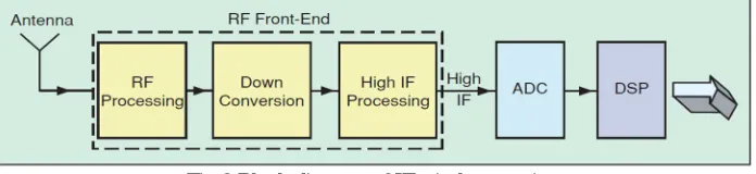
A generic wireless receiver consists of an antenna, an RF/IF (Intermediate frequency) front-end, an ADC, and a digital signal processor (DSP) [2], as shown in Figure 1
Technology (IJRASET)
[image:3.612.133.481.81.161.2]©IJRASET: All Rights are Reserved
468
Fig.2 Block diagram of IF wireless receiver
Depending on the receiver architecture, the ADC has to digitize an RF, IF, or baseband signal. The location of the ADC in a receiver chain is very important as it affects the overall performance, complexity, power dissipation, size, and cost. By plant the ADC close to the antenna, functions such as filtering and frequency translation are performed in digital Domain, which reduces the complexity of the receiver and increases the flexibility. A flexible receiver consists of a digitally controlled analog front-end software-defined radio (SDR) and a programmable digital back-end. The digital back-end processes the signals and feeds back control signals that can reconfigure, statically between different standards or dynamically within the same standard, the building blocks in the front-end. These blocks then switch to a different set of performance values (a different filter order or cut-off frequency for a filter, or a different gain and bandwidth for a low-noise amplifier, or a different gain for a variable gain amplifier, or different dynamic range and bandwidth for an ADC, etc.).
II. SYSTEMARCHITECTURE
A band-pass sigma-delta modulator is more attractive because it can achieve higher resolution while consuming less power [3]. It is a promising candidate for its superior inherent features at high frequencies. In band-pass ΣΔ modulator the quantization noise is
attenuated only in narrowband, thus taking advantage of a high OSR to achieve high DR requirements. The band-pass ΣΔ modulator can be used to digitize signals in the baseband.
Figure3 illustrates a typical block diagram of the IF-to-baseband section in a digital receiver based on a BP sigma delta modulator. As shown, the band pass sigma delta modulator contains a band pass loop filter H(z) for obtaining a stop-band NTF with zeros placed at a nonzero frequency, referred to as the notch frequency fn. The digital output of the modulator is mixed to DC by a digital quadrature mixer and then LP filtered and decimated by a quadrature decimation filter to remove out-of-band spectral components and quantization noise. The resulting baseband digital data are finally processed in a DSP [4].
[image:3.612.126.487.440.560.2]
Fig. 3. Typical section of an IF-conversion receiver based on a BP sigma delta ADC.
III. NONIDEALITIES
There are some non-idealities which affects the performance of sigma-delta modulator:
A. Sampling jitter
Sampling jitter results in non-uniform sampling and increases the total error power in the quantizer output. The magnitude of this error is a function of both the statistical properties of the jitter and the input signal to the converter.
Consider a signal ( ) being sampled by clock signal which has jitter, producing an error in time . From the definition of derivative we can write
( ) ( )
≈ (1)
Technology (IJRASET)
©IJRASET: All Rights are Reserved
469
Where is the error associated with jitter. From this expression, the equation for the imperfect signal will be, ( + ) = + ( ) (3)
or, ( + ) = ( )+ (4)
This effect can be simulated with SIMULINK by using the model shown in Fig.4,
Fig. 4. Modeling a random sampling jitter B. Thermal noise
Thermal noise generates by the random fluctuation of carriers because of thermal energy. Fig.5 shows single ended switched capacitor. CS is the sampling capacitor which is periodically charged and discharged by four switches. CS is in series with a switch with ON resistance Ron which injects a noise voltage
onto the capacitor. This is often known switch thermal noise. The total noise power can be describe by as follows
Fig.5 Single-ended SC integrator
=∫
( ) = (5)
where is the Boltzmann constant and T is the absolute temperature.
C. Opamp noise
Opamp noise model is shown in fig.6 which is used to simulate the effect of noise. From the figure Vn represents the total rms noise voltage. Flicker (1/f) noise, wide-band thermal noise and dc offset contribute to this value. The total op-amp noise power can be evaluated, through circuit simulation, during phase 2, by adding the noise contributions of all the devices referred to the op-amp input and integrating the resulting value over the whole frequency spectrum.
Technology (IJRASET)
©IJRASET: All Rights are Reserved
470
D. Slew rate and bandwidth
Slew rate is the maximum rate of change of output voltage per unit of time. The slew rate is inherently limited by the small internal drive currents of an op-amp but is also limited by internal capacitance designed to compensate against high frequency oscillations. Some op-amps are externally compensated and therefore offer some control over the slew rate. Slew rate and gain bandwidth is defined by:
SR=max ( ) (6) GBW = 2 ≤ => = (7) The effect of the finite gain bandwidth and the slew-rate are related to each other and may be interpreted as a non-linear gain.
IV. SIMULATIONRESULT
A. Design Flow Diagram
Fig.7 shows the design flow diagram of proposed work which consists of some steps to Execute the overall work. Firstly start the process of our method by using GUI. In GUI choose the parameters like oversampling ratio, bandwidth and number of samples, then apply the insertion of the nonidealities. After this simulink model can be constructed using SD toolbox. Parameter like SNDR and ENOB can be calculated using matlab. If enhance the value then go for next otherwise repeat the process by changing the input values. If we find the improved value then stop the process.
Technology (IJRASET)
©IJRASET: All Rights are Reserved
471
B. Experimental Setup
The basic GUI performs the following function
1) Inputs: fig.8 shows the basic GUI diagram.In this diagram it is clearly shown that 3 inputs namely Bandwidth, Oversampling Ratio(R) & No. of Samples (N) is inputted.
2) Simulink model: After applying the inputs the Open Simulink Model Tab will open the simulink model as shown in fig.9. 3) Outpus: After the simulink model runs we will get the output in the GUI
Fig.8. Basic GUI diagram
Technology (IJRASET)
©IJRASET: All Rights are Reserved
472
Outputs
Fig.10. GUI showing the output waveforms
Fig.11 shows the power spectral density waveform with respect of frequency. From this waveform we got the value of SNDR and ENOB of 42.9 and 6.84. We can get the improved waveform by changing the value of input parameters.
Technology (IJRASET)
©IJRASET: All Rights are Reserved
473
Table 1 Various Parameters Result
Fs(Hz) 42800000
Ts(s) 2.336449e-008
Fin(Hz) 10741798.8750
Bw(Hz) 200000
OSR 107
Npoints 4096
tsim(sec) 0.00
Nperiods 1028.00
SNR(dB) 42.6
Simulation time 0.045 min
ENOB 6.84 bits
[image:8.612.122.490.87.294.2]SNDR 42.9
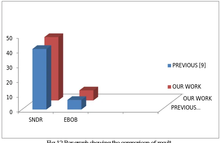
Table 2: Comparing the value of our work with previous work Parameter Previous [5] Our work
Bandwidth 20M 200K
GBW 400MHz 400MHz
Slew rate 340V/us 340V/us
SNDR 41dB 42.9dB
ENOB 6.51bits 6.84bits
[image:8.612.128.490.402.636.2]Table 2 shows thecomparing the value of our work with previous work [5]. From this table we can see that in our work the value of SNDR and ENOB is improved comparing with previous work. Fig.12 shows bar graph of this comparison.
Fig.12 Bar graph showing the comparison of result
V. CONCLUSION
This thesis concerns discrete-time 2nd order band-pass sigma-delta modulators targeted for analog-to-digital (A/D) conversion in wireless receivers. The receiver architecture adopted has to be capable of operating with different radio frequencies, channel bandwidths, and modulation techniques. This is necessary in order to achieve an extensive operating area and the possibility of utilizing a local mobile phone standard or a standard suitable for a specific service. The digital IF receiver is a good choice for a
Technology (IJRASET)
©IJRASET: All Rights are Reserved
474
multi-mode and multi-band mobile phone receiver, because the signal demodulation and channel filtering are performed in the digital domain. This increases the flexibility of the receiver and relieves the design of the baseband part, but an A/D conversion with high dynamic range and low power dissipation is required. BP sigma-delta modulators are capable of converting a high-frequency narrow band signal and are therefore suitable for signal digitization in an IF receiver.
A GUI based implementation has been made to calculate the SNDR and ENOB. In this thesis we found that by implementing this technique we found a better SNDR and ENOB with better performance.The value of SNDR and ENOB are found to be 42.9 dB and 6.84 bits respectively in comparison to the 41dB & 6.51bits respectively of the previous work. Since the value of SNDR and ENOB are increased it makes the respective signal power and Resolution better
REFERENCES
[1] T. K. Bandopadyay , Manish Saxena, Raghav Shrivastava Sigma Delta Modulator with Improved Performance through Evolutionary Algorithm International Journal of Science and Research (IJSR) Volume 2 Issue 3, March 2013
[2] Rusu, A., Dong, B., & Ismail, M. (2006). Putting the" FLEX" in flexible mobile wireless radios-A wideband continuous-time baudpass sigma-delta ADC software radios. Circuits and Devices Magazine, IEEE, 22(6), 24-30.
[3] Nagaraj, P., & Yellampalli, S. (2013). 8 Bit Second-Order Continuous-Time Band-Pass Sigma-Delta ADC. International Journal of Innovative Technology and Exploring Engineering (IJITEE),3(1), 2278-3075.
[4] Converters, C. S. D., & Guide, P. D. (2013). Introduction to Modulators: Basic Concepts and Fundamentals.
[5] Chang, H., Lu, W., Cheng, X., Guo, Y., & Zeng, X. (2011, October). Modeling of a double-sampling switched-capacitor bandpass delta-sigma modulator for multi-standard applications. In ASIC (ASICON), 2011 IEEE 9th International Conference on (pp. 465-468). IEEE.
[6] Lim. H. J.,Sheung. S.,Ng. Y. and Je. M. (2013). Bandpass Continuous Modulator for Wireless Receiver IC. International Journal of Information and Electronics Engineering. 3(1).
[7] Ahmad G., Baghel Dr. R. K. (2010). Jitter Analysis of Continuous-Time Sigma-Delta Wideband ADC for Software Defined Radio. International Journal of Engineering Science and Technology Vol. 2(9), 2010, 4336-4341
[8] Tortosa, R., de la Rosa, J. M., Rodríguez-Vázquez, A., & Fernández, F. V. (2005, May). Analysis of clock jitter error in multibit continuous-time ΣΔ
modulators with NRZ feedback waveform. In Circuits and Systems, 2005. ISCAS 2005. IEEE International Symposium on (pp. 3103-3106). IEEE.
[9] Brigati, S., Francesconi, F., Malcovati, P., Tonietto, D., Baschirotto, A., & Maloberti, F. (1999, July). Modeling sigma-delta modulator non-idealities in SIMULINK (R). In Circuits and Systems, 1999. ISCAS'99. Proceedings of the 1999 IEEE International Symposium on (Vol. 2, pp. 384-387). IEEE.
[10] Jaydip.H.Chaudhari, Gireeja D.Amin Design and Simulation of 1-bit Sigma Delta ADC in 0.18um CMOS Technology International Journal of Computer Applications & Information Technology Vol. II, Issue I, January 2013
[11] Y. Zhu, S.F. Al-Sarawi, C. C. Lim, and M.J. Liebelt Fourth-Order Discrete-Time Variable Centre Frequency Bandpass Sigma-Delta Modulator IEEE 2006 [12] Shaoyu MA, Yan Han, You Cai A 3.3V 18 Bit Digital Audio Sigma- Delta ADC in 0.18 um CMOS Process 2007
[13] Mingyuan Ren, Tong Wu, Changchun Dong, Linghai Cui. The Design of High Performance, High Resolution Two-Order Delta-Sigma Modulator. Sensors &Transducers,Vol.22,Special Issue, June 2013, pp.155-162.
[14] Kumar, Y. B. N., Caracciolo, H., Bonizzoni, E., Parra, A., & Maloberti, F. (2013, May). A 1.96-mW, 2.6-MHz bandwidth discrete time quadrature band-pass
ΣΔ modulator. In Circuits and Systems (ISCAS), 2013 IEEE International Symposium on (pp. 1998-2001). IEEE