I n t e r n a t i o n a l J o u r n a l o f E n g i n e e r i n g R e s e a r c h a n d S p o r t s S c i e n c e Page1
S Nagakishore Bhavanam
Assistant Professor, University College of Engineering & Technology,Acharya Nagarjuna University, Guntur, A.P.,INDIA
Dr. P. Siddaiah DEAN, University College of Engineering & Technology Acharya Nagarjuna University, Guntur, A.P., INDIA
Vasujadevi M Assistant Professor, Chalapathi Institute of Engineering & Technology Guntur, A.P., INDIA
ABSTRACT
The inherent property of patch antenna is its narrow bandwidth, typically a few percent. To improve the impedance bandwidth characteristics of the patch antenna the ground shape is modified. This letter focuses on single layer printed compact rectangular patch fed by a microstrip feed line and a partial ground plane for X– Band applications. The FR4 with ℇr = 4.6 is selected as substrate and its total size is 30 mm× 22 mm. To improve the Impedance Bandwidth of the antenna a rectangular slot on patch and the modified ground plane with semielliptical shaped slots on its top edge are
incorporated. The impedance Band width of the antenna with and without slots are compared. The Simulation studies are carried in the X band using Electromagnetic Simulator HFSS -14.0 version.
__________________________________________________________________________________________________________
I. INTRODUCTION
The antennas required for the various applications should be of small size, lightweight, low profile, broad bandwidth, low cost and integrable with MIC/MMIC circuits[1-5]. The major disadvantages of Microstrip antenna is narrow bandwidth, poor efficiency and size [6]. For efficient
radiation, the size of Microstrip antenna should be λ/2. If the size reduces less than λ/2, the radiation efficiency of antenna
decreases along with other antenna parameters. The miniaturization of antenna and improvement in bandwidth can be achieved by etching the slot in ground and patch of Microstrip antenna of proper length and width [7-9]. This paper concentrates on the effect on antenna resonant frequency and other antenna parameters due to slots in patch and ground plane to design the compact antenna with improved bandwidth and efficiency.Due to its high data transmission rate, large bandwidth, and short-range characteristics, X band technology has been widely used in various applications Designing X band antennas to match these applications is still a major challenge and has attracted the interest of many researchers [4,5]. Despite X band performance, the antennas proposed in [4] and [5]are not suitable to integrate into printed circuit boards owing to their large size and the manufacturing difficulties. Having its low cost, low profile, ease of fabrication and wide band-width, the printed planar structure appears to be the most promising candidate for wideband applications. Recently, various planar antennas have been proposed and investigated because of
their advantages [6 –9]. For example, a small UWB elliptical ring antenna fed by a coplanar waveguide has been proposed and investigated in [10]. A microstrip line of width 3 mm is printed on the same side of the patch on the substrate as the radiator. The finite partial ground plane with initial dimensions of 30 × 7.5 mm is printed on the bottom side of the substrate shown in figure 1. The length of microstrip line is fixed at 7.25 mm to achieve 50 ohms characteristic impedance. Multibands obtained between 3.68 GHz to 5.22 GHz, 6.3 GHz to -8.67 GHz,9.25 GHz to 10.4 GHz, 12.7 GHz to 18.464 GHz .The geometric parameters of the proposed antenna structure can be adjusted to tune the VSWR as well as the bandwidth over a wide range of frequencies. To improve the bandwidth of the proposed antenna, the ground plane is modified by cutting Semi- elliptical shaped slots on its top edge is shown figure2.. From the optimization of antenna parameters it is found that the antenna is capable of tuning from 3.1 GHz to 4.8 GHz, 5.8 GHz to 12.8 GHz, 13.2 GHz to 15 GHz and 16 GHz to 19.5GHz . To improve the bandwidth more of the proposed antenna, design2 is modified into design3 by a slot cut in radiating patch with length and width 10 mm x 1 mm. Compared to the antenna having no slots in the ground plane, the antenna with semi elliptical shaped slots on the top edge of the ground plane can enhance the bandwidth. By insertion of slots on the top edge of the ground plane increases the gap between the radiating patch and the ground plane, resulting in enhancement of impedance bandwidth.
PRINTED MICROSTRIP COMPACT ANTENNA
WITH SLOTS IN GROUND PLANE AND PATCH
USING HFSS
ENGINEERING
I n t e r n a t i o n a l J o u r n a l o f E n g i n e e r i n g R e s e a r c h a n d S p o r t s S c i e n c e Page2 II. DESIGN OF RECTANGULAR MICROSTRIP
PATCH
Rectangular Microstrip patch has been designed on ℇr is
4.6 and thickn ess h = 1.53 mm. It is decided to design the rectangular patch for 8GHz to 12 GHz. For a dielectric substrate of thickness 'h', relative dielectric constant ℇr and antenna operating frequency f0. For the
efficient antenna the width and length of the patch can be calculated by
- 1
-∆L - 2
Where, , ∆L can be calculated from [8]. The antenna
has also been designed using electromagnetic simulator
III. ANTENNA CONFIGURATION
The configuration of the initial design[1-2] and [4-9] of the proposed antenna is shown in figure 1a . The radiating patch, which has a compact size of 14.75 mm× 14.5 mm is printed on the top side of an FR4 PCB substrate of thickness 1.6 mm and relative permittivity of ℇr = 4.6. It is obvious that the measured gain is higher than the gain of those antennas reported earlier in [5] and [6]. A microstrip line of width 3 mm is printed on the same side of the patch on the substrate.
Figure 1a. Microstrip Antenna without slots and with finite ground. All the Units are in
mm.
Figure 1b. Microstrip Antenna with finite ground and slots on ground. All the Units are in mm.
Figure 1c. Microstrip Antenna with slots in ground and in patch with finite ground. All the Units are in mm.
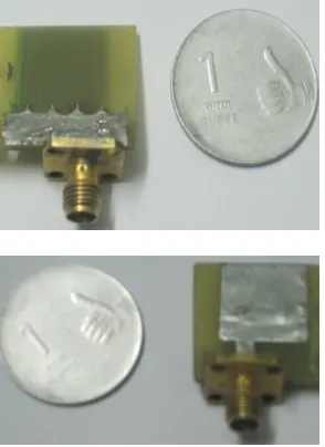
Figure 1d. Photograph of the proposed antenna front and back views of of Microstrip Antenna with semi elliptical slots in
I n t e r n a t i o n a l J o u r n a l o f E n g i n e e r i n g R e s e a r c h a n d S p o r t s S c i e n c e Page3 The finite partial ground plane with initial dimensions of
30mm × 7.5 mm is printed on the bottom side of the substrate. The length of microstrip line is fixed at 7.25 mm to achieve 50 ohms characteristic impedance. Between the patch and the ground plane there is an overlap of 0.25 mm. Photograph of the front and back views of of Microstrip Antenna with semi elliptical slots in finite ground is shown in the figure 1.d.The geometric parameters of the proposed antenna structure can be adjusted to tune the Return Loss as well as the bandwidth over a wide range of frequencies. To improve the bandwidth of the proposed antenna, the ground plane is modified by cutting semi-elliptical shaped slots on its top edge. The semielipptical slot major axis and minor axis are 10mm X 1mm. The resultant ground plan e with a symm etr ical shaped edge is shown in figure 1.b. To improve more the bandwidth of the proposed antenna a rectangular slot is cut in radiating patch as shown in figure1.c. Compared to the antenna having no slots in the ground plane, the antenna with insertion of shaped slots on the top edge of the ground plane got enhanced due to increase in the gap between the radiating patch and the ground plane in design2. The antenna is optimised by HFSS simulation software. In design 3 due to insertion of rectangular slot in radiating patch Bandwidth further increased.
IV.RESULTS AND DISCUSSION
The simple rectangular microstrip patch antenna of the proposed antenna were designed on a FR4 substrate ℇr = 4.6 and h = 1.6 mm. The dimensions of the micro strip patch have been taken as L x W = 14.75 mm x 14.5 mm at the fundamental resonant frequency of f0 =4.72 GHz. For Design
1 with partial ground and with out slots Multiband occur between 3.68 GHz to 5.22 GHz, 6.3 GHz to -8.67 GHz,9.25 GHz to 10.4 GHz and 12.7 GHz to 18.464 GHz. In design2 semi-elliptical slots are cut in ground plane to improve impedance bandwidth below -10 db are between 3.1 GHz to 4.8 GHz, 5.8 GHz to 12.8 GHz, 13.2 GHz to 15 GHz and 16 GHz to 19.5GHz) with maximum return loss -25 dB with centre frequency 7 GHz, and bandwidth is 85.7% in X Band. In design3 with Slots in ground plane and in patch Impedance Bandwidth of below -10db obtained for the bands 3.1 GHz to 4.8 GHz, 6.1 GHz to 20 GHz with a maximum Return loss of -29 dB with centre frequency 6 GHz and bandwidth obtained from 6.1 GHz to 20GHz is 13.9 GHz with 231%. Simulated return Loss characteristics for 3 designs are shown in fig 2.1. Experimental Return loss results are shown in fig 2.1 for design 3 with slot in patch and ground plane.
0 2 4 6 8 10 12 14 16 18
-25 -20 -15 -10 -5 0 Frequency inGHZ R e tu rn l o s s ( d B )
With slots in ground plane
and in radiation patch (Design3) With slots in ground plane only (Design2)
With out slots (Design 1)
Figure 2.1 Return loss for proposed antenna – Simulated result
Figure 2.2 Return loss for proposed antenna – Experimental Result
In the X band Return loss is less than -10dB. From 5GHz to 13GHz return loss is below -10 dB with bandwidth 260 %. The Experimental results are coinciding with the simulation results. Gain characteristics for 3 designs shown in figure 3. Maximum gain of 4.5 dB occurred in design1. For Design 2 the maximum gain is 6dB and for design 3 maximum gain is 5.9 dB. Performance parameters are shown in table 1.
0 2 4 6 8 10 12 14 16 18 20
-14 -9 -4 1 6 G a in [ d B ]
With slots in both ground and patch(Design 3) with slots in ground only(Design 2)
With out slots(Design 1)
I n t e r n a t i o n a l J o u r n a l o f E n g i n e e r i n g R e s e a r c h a n d S p o r t s S c i e n c e Page4 and 2. The radiation patterns of slotted ground and slotted
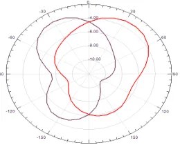
radiation patch antenna are shown in figure4a to 4e for specified frequencies of 8 GHz to 12 GHz. The 3D radiation patterns are shown in figure 5a to 5.e. Although some dips observed the radiation patterns through out the X band are quite stable.
Figure 4a.2D Radiation pattern at 8 GHz (Eplane-red, Hplane – brown)
Figure 4b.2D Radiation pattern at 9 GHz (Eplane-red, Hplane – brown)
Figure 4c.2D Radiation pattern at 10 GHz (Eplane-red, Hplane – brown)
Figure 4d.2D Radiation pattern at 11 GHz (Eplane-red, Hplane – brown)
Figure 4e.2D Radiation pattern at 12 GHz (Eplane-red, Hplane – brown)
I n t e r n a t i o n a l J o u r n a l o f E n g i n e e r i n g R e s e a r c h a n d S p o r t s S c i e n c e Page5 Figure 5. Radiation patterns at 8 GHz,9 GHz ,10 GHz, 11
GHz, 12GHz Frequeny GHz Return. Loss (dB) Band Width in
GHz
Gain (dB) % η
8 -10
6.5 to 7.8, 10.2 to 10.8 13.5
to 17.5
6.12 88.84
9 -10 6.2 to 7.8 , 10 to11.2 ,13.5 to 17
6.2 93.27
10 -10 6.5 to 7.2, 10.1 to
6.21 91.55
11 -10 6.2 to 7.8, 10 to11.2, 13.5 to 17
6.22 98.10
12 -10 5.2 to 7.9, 10.1 to
11.9
6.12 92.45
εr = 4.6, h = 1.53mm, L = 14.5mm,
W = 14.75mm
Table 1: Performance comparison of the proposed antenna with different solution frequency with out slots in ground plane
Frequeny GHz Return. Loss (dB) Band Width in GHz Gain (dB) % η
8 -23
6.5 to 7.8, 10.2 to 10.8 ,
13.5 to 17.5
6.12 0.99
9 -13
6.2 to 7.8 , 10 to11.2 ,13.5
to 17
8.4 1.05
10 -25 6.5 to 7.2, 10.1 to 11.6,
13.5 to 16.6
8.47 0.997
11 -13
6.2 to 7.8 ,
10 to11.2, 13.5 to 17
8.47 0.98
12 -16.5 5.2 to 7.9, 10.1 to 11.9
8.4 1.05
Table 2: Performance comparison of the proposed antenna with different solution
frequency
εr = 4.6, h = 1.53mm, L = 14.5mm, W = 14.75mm
V. CONCLUSION
A printed compact antenna has been proposed and simulated using HFSS. The antenna having a total size of 30 × 22 mm, FR4 PCB substrate. The modified ground plane with semi-elliptical shaped slots on the top edge helps to increase the impedance bandwidth. It is observed from measurement that the proposed antenna with the modified finite ground plane has achieved an impedance bandwidth return loss -10dB from 6.4 GHz to 1 3 . 6 GHz and a maximum gain of 6 dBi., in entire X band. E x p er i m en ta l R et u r n l oss m ea su r em en t s sh o w t h e i m p ed a n ce ba n d wi d t h fr om 5 GHz t o 1 3 G Hz wi t h p er cen t a g e ba n d wi d t h of 2 6 0 % . The symmetric and stable radiation pattern with an average gain of 6 dB makes the proposed antenna uitable for use in X band applications.
REFERENCES
[01] R. Azim, M.T. Islam and N. Misran, Ground modified double-sided printed compact UWB antenna, ELECTRONICS LETTERS 6th January 2011 ,Vol. 47,No. 1
[02] Raj Kumar1, J. P. Shinde and M. D. Uplane, International Journal of Recent Trends in Engineering, Vol 2, No. 6, November 2009, Effect of Slots in Ground Plane and Patch on Microstrip Antenna Performance
[03] Verbiest, J.R., and Vandenbosch, G.A.E.: ‘A novel small-size printed tapered monopole antenna for UWB WBAN’, IEEE Antennas Wirel. Propag. Lett., 2006, 5, (1), pp. 377 – 379
[04] See, T.S.P., and Chen, Z.N.: ‘An electromagnetically coupled UWB plate antenna’, IEEE Trans. Antennas Propag., 2008, 56, (5), pp. 1476 – 1479
[05] Zhou, H., Liu, Q., Sun, B., and Yang, Y.: ‘A band-notched swallow- tailed planar monopole antenna for UWB application’, Microw. Opt. Technol. Lett., 2008, 50, (3), pp. 793 – 795
[06] Kiminami, K., Hirata, A., and Shiozawa, T.: ‘Double-sided printed bow- tie antenna for UWB communications’, IEEE Antennas Wirel. Propag. Lett., 2004, 3, pp. 152 – 153 [07] Ren, Y.J., and Chang, K.: ‘An annual ring antenna for UWB communications’, IEEE Antennas Wirel. Propag. Lett., 2006, 5, (1), pp. 274 – 276
[08] Xiao, J.X., Wang, M.F., and Li, G.J.: ‘A ring monopole antenna for UWB application’, Microw. Opt. Technol. Lett., 2010, 52, (1), pp. 179 – 182
[09] Liu, J., Gong, S., Xu, Y., Zhang, X., Feng, C., and Qi, N.: ‘Compact printed ultra-wideband monopole antenna with dual band-notched characteristics’, Electron. Lett., 2008, 44, (12), pp. 710 – 711
I n t e r n a t i o n a l J o u r n a l o f E n g i n e e r i n g R e s e a r c h a n d S p o r t s S c i e n c e Page6 elliptical ring antenna’,Electron. Lett., 2006, 8, (8), pp. 447 –
449