University of Warwick institutional repository: http://go.warwick.ac.uk/wrap
A Thesis Submitted for the Degree of PhD at the University of Warwick
http://go.warwick.ac.uk/wrap/62126
This thesis is made available online and is protected by original copyright. Please scroll down to view the document itself.
for High Voltage Applications
Craig Arthur Fisher
School of Engineering
University of Warwick
Dissertation submitted for the degree of
Doctor of Philosophy
List of Figures x
List of Tables xi
Declaration xi
Acknowledgements xiii
Publications xv
Abstract xix
List of Abbreviations and Symbols xx
1 Introduction 1
1.1 Background . . . 4
1.2 Motivation . . . 5
1.3 Thesis Outline . . . 6
2 Power Electronics and Silicon Carbide 8 2.1 The Power Grid . . . 9
2.1.1 Power Generation . . . 10
2.1.2 Power Transmission . . . 11
2.1.3 Power Distribution and the End-User . . . 15
2.1.4 The “SmartGrid” Concept . . . 16
2.2 Power Electronics for Transmission Systems . . . 19
2.2.1 Requirements for Power Electronics Devices . . . 19
2.2.2 Thyristors and LCC Transmission . . . 21
2.2.3 IGBTs and SCC Transmission . . . 26
2.2.4 The Role of the PiN Diode . . . 29
2.3 Silicon Carbide for Power Electronics . . . 29
2.3.2 Polytypes of Silicon Carbide . . . 33
2.3.3 Thermal and Electrical Properties of Silicon Carbide . . . 35
2.3.4 Bulk Material Challenges . . . 41
2.3.5 Current Status of Silicon Carbide Power Devices . . . 45
2.3.6 So, Why 4H-SiC? . . . 48
2.4 Summary . . . 49
3 High Voltage 4H-SiC PiN Diode Technical Discussion 51 3.1 PiN Diode Operating Principles . . . 52
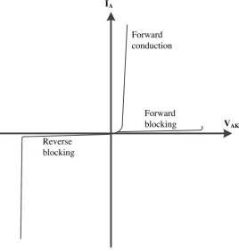
3.1.1 Forward Conduction . . . 52
3.1.2 Reverse Blocking . . . 63
3.1.3 Reverse Recovery Behaviour . . . 68
3.2 High Voltage Junction Termination . . . 74
3.2.1 Floating Field Rings . . . 78
3.2.2 Field Plate Termination . . . 80
3.2.3 Bevel Edge Termination . . . 81
3.2.4 Junction Termination Extension . . . 82
3.2.5 Surface Passivation . . . 86
3.3 Carrier Lifetime in High Voltage 4H-SiC Devices . . . 87
3.3.1 Carrier Recombination: A Quantitative Analysis . . . 87
3.3.2 The Effect of Electrically Active Defects on Carrier Lifetime . . . . 90
3.3.3 Carrier Lifetime Enhancement . . . 92
3.4 4H-SiC Device Fabrication Technology . . . 94
3.4.1 Etching of 4H-SiC . . . 94
3.4.2 Ion Implantation and Activation Annealing . . . 95
3.4.3 Ohmic Contacts to 4H-SiC . . . 98
3.5 A Review of High Voltage 4H-SiC PiN Diode Technology . . . 100
3.6 Summary . . . 104
4 Design and Simulation of High Voltage 4H-SiC PiN Diodes 106 4.1 Numerical Simulation Models . . . 107
4.1.1 Band Gap Narrowing . . . 107
4.1.2 Carrier Transport . . . 111
4.1.3 Incomplete Ionisation . . . 114
4.1.4 Carrier Recombination and Generation . . . 116
4.1.5 Impact Ionisation . . . 118
4.2 4H-SiC PiN Diode Drift Region Design . . . 119
4.3 Simulation of the Forward Characteristics of 4H-SiC PiN Diodes . . . 122
4.4 High Voltage Edge Termination Design . . . 124
4.5 Summary . . . 142
5 Characterisation Techniques for High Voltage 4H-SiC PiN Diodes 144 5.1 Electrical Characterisation . . . 144
5.1.1 Forward I-V Measurements . . . 144
5.1.2 Reverse Breakdown Characterisation . . . 145
5.1.3 High Voltage Inductive Switching Characterisation . . . 146
5.1.3.1 Carrier Lifetime Extraction Method . . . 149
5.1.4 Contact Resistance Measurements . . . 150
5.2 Physical Characterisation . . . 154
5.2.1 Scanning Electron Microscopy . . . 154
5.2.2 Transmission Electron Microscopy . . . 157
5.2.3 Atomic Force Microscopy . . . 158
5.2.4 X-Ray Diffraction . . . 159
5.2.5 Secondary Ion Mass Spectrometry . . . 162
5.2.6 Raman Spectroscopy . . . 164
5.3 Summary . . . 165
6 Fabrication Process Development for 4H-SiC PiN Diodes 166 6.1 RIE and ICP Etching Characterisation . . . 166
6.2 P-type Ohmic Contact Study . . . 170
6.2.1 Fabrication Process for TLM Structures . . . 171
6.2.2 Electrical Characterisation Results . . . 173
6.2.3 TEM / SEM Analysis . . . 177
6.2.4 XRD Analysis . . . 184
6.2.5 Current Transport Mechanisms in P-type Ohmic Contacts . . . 186
6.3 Benchmarking of P-type Ohmic Contact Results . . . 191
6.4 Summary . . . 193
7 Fabrication and Characterisation of 3.3 kV 4H-SiC PiN Diodes 196 7.1 Photomask Design . . . 197
7.2 Device Structures . . . 197
7.3 First Generation 4H-SiC PiN Diodes . . . 199
7.3.1 Fabrication Process . . . 199
7.3.2 Forward I-V Characterisation Results . . . 200
7.3.3 Reverse I-V Characterisation Results . . . 206
7.3.4 The Impact of a Metal Overlayer on Forward I-V Characteristics . . 206
7.4 Second Generation 4H-SiC PiN Diodes . . . 209
7.4.1 Fabrication Process . . . 210
7.4.2 Physical Characterisation Results . . . 213
7.4.2.2 Raman Spectroscopy Analysis . . . 218
7.4.2.3 AFM Analysis . . . 221
7.4.3 Reverse I-V Characterisation Results . . . 224
7.5 Summary . . . 229
8 Fabrication and Characterisation of 10 kV 4H-SiC PiN Diodes 234 8.1 Device Structure . . . 235
8.2 First Generation 10 kV 4H-SiC PiN Diodes . . . 235
8.2.1 The Advantages of High Temperature Oxidation . . . 237
8.2.2 Fabrication Process . . . 238
8.2.3 Forward I-V Characterisation Results . . . 238
8.2.4 Reverse I-V Characterisation Results . . . 245
8.3 Second Generation 10 kV 4H-SiC PiN Diodes . . . 245
8.3.1 Novel Combined Thermal Oxidation and Annealing Process . . . . 247
8.3.2 Fabrication Process . . . 248
8.3.3 Forward I-V Characterisation Results . . . 250
8.3.4 Clamped Inductive Switching Characterisation Results . . . 259
8.4 Summary . . . 267
9 Conclusions and Future Work 271 9.1 Conclusions . . . 271
9.2 Future Work . . . 278
9.2.1 Device Modelling and Simulation . . . 279
9.2.2 Device Fabrication . . . 280
9.2.3 Device Characterisation . . . 282
9.3 Final Words... . . 282
A Fundamental Semiconductor Equations 283 B 4H-SiC Wafer Die Cleaning Process 286 B.1 Introduction . . . 286
B.2 Wafer Die Surface Cleaning Process . . . 286
C Standard Photolithography Process 288 C.1 Introduction . . . 288
C.2 Standard Photolithography Process . . . 288
2.1 Applications of power electronics. . . 9
2.2 Comparison of AC and DC transmission system costs. . . 13
2.3 The SmartGrid. . . 18
2.4 Thyristor structure. . . 21
2.5 Thyristor voltage-current characteristics. . . 23
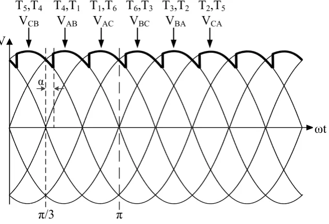
2.6 Schematic of an SCR-based three-phase converter. . . 24
2.7 Operation of a SCR-based three-phase converter. . . 25
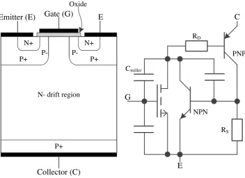
2.8 IGBT structure and equivalent circuit. . . 27
2.9 Crystalline structure and hexagonal packing system of SiC. . . 35
2.10 The hexagonal packing system in SiC. . . 36
2.11 Polytypes of SiC. . . 37
2.12 Theoretical unipolar limits of Si, 3C-SiC and 4H-SiC. . . 39
2.13 Cross sectional view of a micropipe emanating from the substrate and prop-agating into the epitaxial layer. . . 43
2.14 Propagation of substrate defects into epitaxial layer. . . 44
3.1 The PiN diode at zero bias, forward bias and reverse bias. . . 53
3.2 Calculated charge distribution in Si and 4H-SiC PiN diodes. . . 57
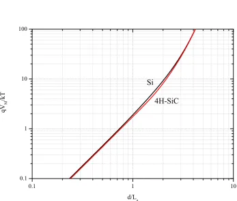
3.3 Drift region voltage drop as a function ofd/La for Si and 4H-SiC PiN diodes. 58 3.4 F(d/La) plotted for Si and 4H-SiC PiN diodes. . . 60
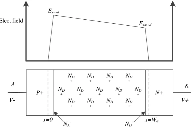
3.5 One-dimensional approximation of the electric field distribution of the PiN diode under reverse bias. . . 65
3.6 Reverse recovery approximation waveforms with inductive load switching. . 70
3.7 Carrier storage region profile and corresponding 1-D electric field distribu-tion during reverse recovery. . . 71
3.8 The two-dimensional (cylindrical) P+/N− junction. . . 76
3.9 Calculated cylindrical and spherical breakdown of a 4H-SiCP+/N− junc-tion. . . 77
3.10 Schematic of implanted P+ floating field ring termination. . . 79
3.11 Field plate termination for a planarP+/N− junction. . . 80
3.13 Junction termination extension applied to an epitaxial anode PiN diode. . 83
3.14 Optimum carrier lifetime in 4H-SiC for a range of drift region widths. . . . 88
3.15 Schematic of cross-section of SM-TZ-JTE structure. . . 104
4.1 Electronic band structure for 2H, 4H- and 6H-SiC. . . 109
4.2 Effect of temperature on the band gap energy of 4H-SiC. . . 110
4.3 Effect of dopant concentration on band edge displacement for n- and p-type
4H-SiC. . . 112
4.4 Effect of dopant concentration on the electron and hole mobilities in 4H-SiC
at 300 K. . . 114
4.5 Effect of temperature on the electron and hole mobilities in 4H-SiC at a
dopant concentration of 1015 cm−3. . . 115
4.6 Electric field profile at breakdown for punch-through and non-punch-through
PiN diode structures. . . 120
4.7 Calculated breakdown voltage as a function of doping concentration in
4H-SiC. . . 121
4.8 Simulated forward J-V characteristics of 3.3 kV PiN diode with varying
carrier lifetime. . . 123
4.9 Simulated forward J-V characteristics of 10 kV PiN diode with varying
carrier lifetime. . . 124 4.10 Simulated forward log(J)-V characteristics of 10 kV PiN diode with varying
carrier lifetime. . . 125 4.11 Structure of 3.3 kV PiN diode used in reverse breakdown simulations. . . . 126 4.12 Electric field distribution at breakdown in unterminated 3.3 kV
mesa-isolated PiN diode. . . 127 4.13 Breakdown voltage versus JTE doping concentration for 3.3 kV SZ-JTE
structures. . . 128 4.14 Breakdown voltage versus JTE doping concentration for 3.3 kV SM-JTE
structures. . . 130 4.15 Schematic of SM-JTE structure in a mesa anode PiN diode. . . 131 4.16 Electric field distribution at breakdown for 3.3 kV 6Z-SM-JTE structure. . 132 4.17 Effect of oxide charge on the breakdown voltage versus JTE doping
con-centration for 3.3 kV 6Z-SM-JTE structure. . . 133 4.18 Schematic of JTE structure with oxide charge under reverse bias conditions.134 4.19 Breakdown voltage versus JTE doping concentration for 10 kV SZ-JTE
and 6Z-SM-JTE structures. . . 135
4.20 Lateral electric field distribution of 10 kV PiN diode with SZ-JTE structure.136 4.21 Lateral electric field distribution of 10 kV PiN diode with 6Z-SM-JTE
structure. . . 137 4.22 Breakdown voltage versus JTE doping concentration for 10 kV SZ-JTE
4.23 Breakdown voltage versus JTE doping concentration for 10 kV quad-zone
JTE structures. . . 139
4.24 Mask layout for quad-zone JTE structure. . . 140
4.25 Breakdown voltage versus JTE doping concentration for 10 kV quad-zone JTE structure with and without sidewall implant. . . 141
5.1 Calibration results for the high voltage reverse breakdown test rig. . . 146
5.2 Schematic diagram of the chopper cell circuit used in the clamped inductive switching test rig. . . 147
5.3 Clamped inductive switching test rig. . . 148
5.4 Transfer length method test structure. . . 151
5.5 Transfer length method plot of total resistance as a function of contact spacing. . . 152
5.6 Transfer length method contact end resistance measurement topology. . . . 153
5.7 Schematic of a scanning electron microscope. . . 156
5.8 Schematic of an atomic force microscope. . . 158
5.9 Diagram illustrating the geometry of crystalline solids associated with Bragg’s Law. . . 161
5.10 Schematic of a typical dynamic SIMS instrument. . . 163
5.11 Energy level diagram showing the states involved in a Raman signal. . . . 165
6.1 ICP etched SiO2 mask patterned using photoresist. . . 169
6.2 ICP etched SiC mesa sidewall with SiO2 mask patterned using photoresist. 170 6.3 ICP etched SiC mesa sidewall with SiO2 and NiV mask (1). . . 171
6.4 ICP etched SiC mesa sidewall with SiO2 and NiV mask (2). . . 172
6.5 Fabricated TLM structures. . . 173
6.6 Rectifying I-V characteristics of unannealed Al/Ti/Al ohmic contact scheme.174 6.7 Specific contact resistance of Ti/Al/NiV ohmic contacts as a function of annealing temperature. . . 176
6.8 Specific contact resistance of Ti/Al/NiV ohmic contacts as a function of annealing time. . . 177
6.9 LR-TEM image of non-annealed Ti/Al/NiV metal scheme. . . 178
6.10 HR-TEM image showing the 4H-SiC/Ti and Ti/Al interfaces. . . 178
6.11 HR-TEM image of the 4H-SiC/Ti interface and the FFT of the crystal structures. . . 179
6.12 HR-TEM image of the Ti/Al interface and the FFT of the Al crystal struc-ture. . . 180
6.13 HR-TEM image of the Al/NiV interface. . . 180
6.14 LR-TEM image of annealed Ti/Al/NiV ohmic contact. . . 181
6.16 SEM image and associated EDAX analysis of annealed Ti/Al/NiV ohmic
contact. . . 183
6.17 XRD spectra of the Al/Ti/Al metal schemes for a range of annealing con-ditions. . . 185
6.18 XRD spectra of the Ti/Al/NiV metal schemes for a range of annealing conditions. . . 186
6.19 Dependence of E00 onNA in 4H-SiC. . . 187
6.20 Contact resistance as a function of measurement temperature for Al/Ti/Al ohmic contacts. . . 189
6.21 Contact resistance as a function of measurement temperature for Ti/Al/NiV ohmic contacts. . . 190
6.22 Contact resistance as a function of measurement temperature for Ti/Al ohmic contacts. . . 191
7.1 Die design for PiN diode fabrication. . . 198
7.2 Epitaxial structures of 3.3 kV 4H-SiC PiN diodes. . . 198
7.3 Forward log(J)-V characteristic of a small-area first generation 3.3 kV 4H-SiC PiN diodes. . . 202
7.4 Differential on-resistance against current density of a small-area first gen-eration 3.3 kV 4H-SiC PiN diode. . . 203
7.5 Ideality factor against voltage of small-area first generation 3.3 kV 4H-SiC PiN diodes. . . 205
7.6 Reverse log(J)-V characteristics of first generation 3.3 kV 4H-SiC PiN diodes.207 7.7 Comparison of Forward log(J)-V characteristic of small-area first-generation 3.3 kV 4H-SiC PiN diodes with and without metal overlayer. . . 208
7.8 Comparison of Forward log(J)-V characteristic of large-area first-generation 3.3 kV 4H-SiC PiN diodes with and without metal overlayer. . . 209
7.9 Implant profile of boron in NiV/SiO2 mask at an implant energy of 360 keV.211 7.10 Simulated implanted box profile of boron in 4H-SiC. . . 213
7.11 Experimental and simulated implanted box profiles of boron in 4H-SiC. . . 214
7.12 Experimental implanted box profiles of boron in 4H-SiC for a range of annealing temperatures. . . 215
7.13 Experimental implanted box profiles of boron in 4H-SiC annealed at 1700◦C with and without capping layer. . . 217
7.14 Raman spectra of high-dose B-implanted samples. . . 220
7.15 Lorentzian fitting parameters for Raman spectra. . . 221
7.16 AFM scan of unannealed 4H-SiC control sample. . . 222
7.17 AFM scans of B-implanted 4H-SiC samples annealed at 1500◦C. . . 223
7.18 AFM scans of B-implanted 4H-SiC samples annealed at 1600◦C. . . 224
7.20 Reverse log(J)-V characteristics of second generation 3.3 kV 4H-SiC PiN diodes with low dose JTE implant. . . 226 7.21 Reverse log(J)-V characteristics of second generation 3.3 kV 4H-SiC PiN
diodes with medium dose JTE implant. . . 227 7.22 Reverse log(J)-V characteristics of second generation 3.3 kV 4H-SiC PiN
diodes with high dose JTE implant. . . 228 7.23 Geometric mean and standard deviation of reverse current density as a
function of annealing temperature of second generation 3.3 kV 4H-SiC PiN diodes. . . 229 7.24 Reverse breakdown characteristics of second generation 3.3 kV 4H-SiC PiN
diodes. . . 230 7.25 Reverse breakdown voltage as a function of annealing temperature of
sec-ond generation 3.3 kV 4H-SiC PiN diodes. . . 231
8.1 Epitaxial structure of 10 kV 4H-SiC PiN diodes. . . 235
8.2 Defect map for 10 kV 4H-SiC epitaxial wafer. . . 236
8.3 Forward J-V characteristics of small-area first generation control sample
10 kV PiN diode. . . 239
8.4 Forward log(J)-V characteristics of small-area first generation control
sam-ple 10 kV PiN diode. . . 240
8.5 Differential on-resistance of small-area first generation control sample 10 kV
PiN diode. . . 241
8.6 Differential on-resistance of large-area first generation control sample 10 kV
PiN diode. . . 242
8.7 Ideality factor as a function of current density of small-area first generation
control sample 10 kV PiN diode. . . 243
8.8 Forward J-V characteristics of thermally-oxidised small-area first
genera-tion 10 kV PiN diodes. . . 244
8.9 Reverse log(J)-V characteristics of first generation 10 kV PiN diodes. . . . 246
8.10 Photograph of DCB-mounted second-generation 10 kV PiN diode die. . . . 249 8.11 Forward J-V characteristics of small-area second generation 10 kV PiN
diodes. . . 251 8.12 Forward J-V characteristics of large-area second generation 10 kV PiN diodes.252 8.13 Forward voltage drop as a function of active area of second generation
10 kV PiN diodes. . . 253 8.14 Log(J)-V characteristics of small-area second generation 10 kV PiN diodes. 254 8.15 Ideality factor as a function of current density of small-area second
8.18 Statistical data for the differential on-resistance of DCB-mounted second generation 10 kV PiN diodes. . . 258
8.19 Numerical simulation of current density in PiN diode structures with 1µm
and 10 µm thick metal overlayers. . . 259
8.20 Schematic diagram of the chopper cell circuit used in for clamped inductive switching tests. . . 261 8.21 Inductive switching characteristics of Si diode and Si IGBT - IGBT
turn-off, diode turn-on. . . 262 8.22 Inductive switching characteristics of Si diode and Si IGBT - IGBT
turn-on, diode turn-off. . . 263 8.23 Power and energy dissipation of Si PiN diode over switching cycle. . . 264 8.24 Inductive switching characteristics of SiC control sample PiN diode and Si
IGBT - IGBT turn-off, diode turn-on. . . 265 8.25 Inductive switching characteristics of SiC control sample PiN diode and Si
IGBT - IGBT turn-on, diode turn-off. . . 266 8.26 Power and energy dissipation of 4H-SiC PiN diode over switching cycle. . . 267 8.27 Reverse recovery characteristics of control sample and oxidised / annealed
2.1 Materials properties of various semiconductors . . . 36
3.1 Summary of electrical properties of the extrinsic defects observed in 4H-SiC. 91 3.2 Summary of electrical properties of intrinsic defects observed in 4H-SiC. . . 92
4.1 Band gap narrowing temperature dependence parameters. . . 108
4.2 Band gap narrowing doping dependence parameters. . . 111
4.3 Carrier mobility model parameters. . . 113
4.4 Doping concentration-dependent SRH lifetime model parameters. . . 117
4.5 Impact ionisation model parameters. . . 118
4.6 Dimensions of SM-JTE designs. . . 130
6.1 Summary of etch rates and mask selectivity for RIE/ICP etch processes. . 168
6.2 Summary of electrical characterisation results for Al/Ti/Al p-type contact structures. . . 175
6.3 Comparison of p-type ohmic contact specific contact resistance. . . 192
7.1 Dimensions of first generation 3.3 kV PiN diodes. . . 199
7.2 Ion implantation specifications for 3.3 kV PiN diode JTE. . . 212
8.1 Forward characteristics of small-area first generation 10 kV PiN diodes. . . 244
8.2 Forward characteristics of large-area first generation 10 kV PiN diodes. . . 245
This thesis is submitted to the University of Warwick in support of my application for the degree of Doctor of Philosophy. It has not been submitted for a degree at any other University. Except where specifically stated, all of the work described in this thesis was carried out by the author or under his direction in the School of Engineering at the University of Warwick from October 2010 until February 2014.
C. A. Fisher
First, I would like to thank my PhD supervisor, Professor Philip Mawby,
without whom this PhD would not have been possible. Undertaking this
PhD in the exciting field of power electronics, within the hi-tech electronics engineering environment at the University of Warwick, has provided me with experience that I am hugely grateful for, and, without doubt, Phil is the sole recipient of this gratitude. Again, thank you Phil, I sincerely hope that both our professional and personal relationship can continue in the future.
Next, I have to give huge thanks to my co-supervisor, Dr Michael Jennings. In addition to many insightful conversations and suggestions about the research presented in this thesis, I have also had the pleasure of some interesting so-cial activity with Mike, mostly involving extended evenings out in several of Leamington Spa’s drinking establishments. Mike, for both your technical and social contributions to my time as a PhD student, thank you, no doubt there will be more to come in the future!
I would also like to specially thank Dr Angus Bryant, who’s enthusiasm for and knowledge of the subject of power electronics was a huge inspiration for me, and also motivated me in wanting to undertake a PhD in this field at the University of Warwick. Thank you Angus.
Next, special thanks go to Dr Peter Gammon, who, during the brief overlap-ping time when we were both PhD students in the power electronics research group, allowed me to benefit from his experience and knowledge in the field to become an effective researcher. Since then, Peter has continued to unre-servedly offer his support and guidance, for which I am hugely grateful. I trust that both our professional and personal relationships will continue, at least in the form of the annual Warwick Real Ale Festival and the occasional curry night.
Special thanks also go to Dr Dean Hamilton, for his device packaging and char-acterisation support, Dr Yogesh Sharma, for his semiconductor and cleanroom expertise, Dr Stephen Thomas, for his semiconductor knowledge and critical eye, and Dr Benedict Donnellan, for lending a hand with the numerous finite element modelling problems I encountered.
Thanks also go to other academic collaborators at Warwick, including: Dr Neil Wilson, for his AFM expertise, Dr Ana Sanchez, for her TEM and SEM ex-pertise, Dr Richard Beanland, also for his TEM and SEM exex-pertise, Dr David Walker, for his XRD expertise, Dr Susan Burrows, for her support with laser cutting of SiC material, Jonathan Newland, for device fabrication support, Dr Layi Alatise, for his power electronics knowledge as well as his guidance during my progress panels and, lastly, Professor Julian Gardner, for his guidance and suggestions during my progress panels. Outside of Warwick, I would like to
thank Dr Amador P´erez-Tom´as at CNM-CSIC, for his guidance and
exper-tise in SiC device design, fabrication and characterisation, Dr Owen Guy and his staff at Swansea University, for their device fabrication support, Dr Daniel Wolverson at the University of Bath, for his support with Raman spectroscopy activities, and, finally, Professor Florin Udrea and Dr Nishad Udugampola at Cambridge University, for their device characterisation support.
Adding to the list of acknowledgements to within the University of Warwick, thanks also go to Paul Hedley, Charles Joyce, Joel Whittle, Bill Higgins, Frank Courtney, Gavin Downs, Stewart Edris, Gavin Starkey, Alan Hulme, Graham Canham and John Pillier, for their technical support throughout my PhD, and also to Kerrie Hatton, Sarah Pain, Dean Boni and Steve Jones, for their research / administrative support.
Journal Publications
1. C. A. Fisher, M. R. Jennings, Y. K. Sharma D. P. Hamilton, S. M. Thomas, P. M.
Gammon, A. P´erez-Tom´as, S. E. Burrows and P. A. Mawby
‘Improved performance of 4H-SiC PiN diodes using a novel combined high temper-ature oxidation and annealing process’
Manuscript accepted for publication (subject to revisions) in IEEE Transactions on Semiconductor Manufacturing, April 2014.
2. M. R. Jennings, C. A. Fisher, D. Walker, A. Sanchez, A. P´erez-Tom´as, D. P.
Hamilton, P. M. Gammon, S. E. Burrows, S. M. Thomas, Y. K. Sharma, F. Li and P. A. Mawby
‘Physical and electrical characterisation of 3C-SiC and 4H-SiC for power semicon-ductor device applications’
Physics of Semiconductor Devices, pp. 929-932 (2014).
3. S. Jahdi, O. Alatise, C. A. Fisher, L. Ran and P. A. Mawby
‘An evaluation of silicon carbide unipolar technologies for electric vehicle drive-trains’
Manuscript accepted for publication in IEEE Journal of Emerging and Selected Top-ics in Power ElectronTop-ics, February 2014.
4. S. M. Thomas, Y. K. Sharma, M. A. Crouch, C. A. Fisher, M. R. Jennings and
P. A. Mawby
‘Enhanced field effect mobility on 4H-SiC by oxidation at 1500◦C’
5. C. A. Fisher, M. R. Jennings, A. T. Bryant, A. P´erez-Tom´as, P. M. Gammon, P. Godignon and P. A. Mawby
‘Physical modelling of 4H-SiC PiN diodes’
Mat. Sci. Forum. 717-720, pp. 993-996 (2012).
6. M. R. Jennings, A. P´erez-Tom´as, A. Bashir, A. M. Sanchez, A. Severino, P. J.
Ward, S M. Thomas, C. A. Fisher, P. M. Gammon, M. Zabala, S. E. Burrows,
B. T. Donnellan, D. P. Hamilton, D. Walker and P. A. Mawby
‘Bow free 4” diameter 3C-SiC epilayers formed upon wafer-bonded Si/SiC sub-strates’
Conference Publications
1. C. A. Fisher, M. R. Jennings, Y. K. Sharma, D. P. Hamilton, S. M. Thomas, P. M.
Gammon, A. P´erez-Tom´as, S. E. Burrows and P. A. Mawby
‘On the application of novel high temperature oxidation processes to enhance the performance of high voltage silicon carbide PiN diodes’
Manuscript accepted for presentation at EPE ’14-ECCE Europe, Finland, August 2014.
2. C. A. Fisher, M. R. Jennings, Y. K. Sharma, S. M. Thomas, F. Li, P. M. Gammon,
D. P. Hamilton, A. P´erez-Tom´as, S. E. Burrows and P. A. Mawby
‘On the application of a novel combined implant activation anneal / SiO2passivation
process for 4H-SiC PiN diodes’
Manuscript accepted for presentation at the 56th Electronic Materials Conference (EMC), Santa Barbara, USA, June 2014.
3. C. A. Fisher, M. R. Jennings, Y. K. Sharma, D. P. Hamilton, S. M. Thomas, F. Li,
P. M. Gammon, A. P´erez-Tom´as, S. E. Burrows and P. A. Mawby
‘Enhanced forward bias operation of 4H-SiC PiN diodes using high temperature oxidation’
Manuscript presented at the Materials Research Society (MRS), San Francisco, USA, April 2014.
4. M. R. Jennings, C. A. Fisher, D. Walker, A. Sanchez, A. P´erez-Tom´as, D. P.
Hamilton, P. M. Gammon, S. E. Burrows, S. M. Thomas, Y. K. Sharma, F. Li and P. A. Mawby
‘On the Ti3SiC2 metallic phase formation for robust p-type 4H-SiC ohmic contacts’
Presented at the International Conference on Silicon Carbide and Related Materials (ICSCRM) 2013, Miyazaki, Japan, Sept. 29th - Oct. 4th.
5. P. M. Gammon, C. A. Fisher, V. A. Shah, M. R. Jennings, A. P´erez-Tom´as,
S. E. Burrows, M. Myronov, D. R. Leadley and P. A. Mawby
‘The cryogenic testing and characterisation of SiC PiN diodes’
6. S. M. Thomas, M. R. Jennings, Y. K. Sharma,C. A. Fisher and P. A. Mawby
‘Impact of oxidation temperature on the interface trap density in 4H-SiC MOS capacitors’
Despite the excellent electrical and thermal properties of 4H-silicon carbide (SiC), the fabrication of high-voltage SiC power devices is still proving problematic, being hindered by material defects resulting in low carrier lifetimes and forward voltage drift, and sub-optimum ohmic contacts to p-type material. The PiN diode is one such device that suffers from the aforementioned problems, though at the same time is sought after for high voltage power electronics applications due to the prospect of greatly reduced power losses and increased power handling capability than the Si devices currently in use. As such, this thesis is focussed on the development of these devices, investigating various device structures to achieve high reverse blocking voltages as well as developing novel fabrication processes to improve the electrical performance of the devices.
Electrical characterisation of ohmic contacts to p-type 4H-SiC showed that
Ti/Al-based metal schemes offered the lowest specific contact resistivity of approximately 2.2×
10−6Ω-cm2, which was achieved after annealing at 1000◦C for 2 minutes. Physical analysis
showed that these annealing conditions were optimum for formation of the Ti3SiC2 alloy
at the metal-semiconductor interface, the presence of which was found to correlate with lower specific contact resistivity values. Electrical characterisation of first generation PiN diodes designed for blocking 3.3 kV showed that the fabricated devices had a differential
on-resistance (Ron,dif f) of 17 mΩ-cm2 at 100 A/cm2 and 25◦C, and near-ideal (η = 1.3)
characteristics in the diffusion current regime. Based on the measured reverse saturation currents, the carrier lifetime of the fabricated devices was estimated to be 480 ns. Reverse
leakage currents were found to vary significantly across the devices, from 5 nA/cm2 up to
200 µA/cm2 at 100 V reverse bias and 25◦C. Second generation 3.3 kV PiN diodes, which
featured a B-implanted JTE structure, were found to block a maximum reverse voltage of 2.8 kV, which was around 85% of the target value.
PiN diodes fabricated with a drift region designed for blocking 10 kV underwent
ther-mal oxidation processes at temperatures ranging from 1400◦C to 1600◦C in order to
in-crease the carrier lifetime. Devices having undergone no lifetime enhancement treatment
were found to have a Ron,dif f of 11.6 mΩ-cm2 at 100 A/cm2 and 25◦C, and an ideality
factor η = 1.5 in the diffusion current regime. PiN diodes that had undergone thermal
oxidation were found to have improved forward characteristics, with devices oxidised at
1500◦C exhibiting aRon,dif f of around 9 mΩ-cm2at 100 A/cm2 and 25◦C, an improvement
of nearly 25%. A novel combined thermal oxidation and annealing process was developed
and applied to second generation 10 kV PiN diodes; a mean Ron,dif f of 4.45 mΩ-cm2 was
achieved, and a carrier lifetime of 1.21 µs was extracted from reverse recovery
AC Alternating Current
AFM Atomic force microscopy
BJT Bipolar junction transistor
BPD Basal plane dislocation
CMP Chemical mechanical polishing
CRT Cathode ray tube
CSC Current source converter
DC Direct Current
DFT Density functional theory
DLTS Deep level transient spectroscopy
DUV Deep ultra-violet
EDAX Energy dispersive X-ray analysis
FE Field emission
FEG Field-emission gun
GTO Gate turn-off thyristor
HTCVD High temperature chemical vapour deposition
HVDC High Voltage Direct Current
ICP Inductively coupled plasma
IGBT Insulated gate bipolar transistor
IGSF In-grown stacking fault
JFET Junction field-effect transistor
JTE Junction termination extension
LAGB Low-angle grain boundary
LCC Line-commutated conversion
LED Light-emitting diode
MLC Multi-level converter
MOSFET Metal-oxide-semiconductor field-effect transistor
MZ-JTE Multiple-zone JTE
PT Punch-through
PVT Physical vapour transport
PWM Pulse width modulation
R-G Recombination-Generation
RAF Repeated a-face
RIE Reactive ion etching
RTA Rapid thermal annealing
SBD Schottky barrier diode
SCC Self-commutated conversion
SCR Silicon controlled rectifier
SEM Scanning electron microscopy
SIMS Secondary ion mass spectrometry
SJ Super junction
SM-JTE Space-modulated JTE
SRH Shockley-Read-Hall
SRIM Stopping and range of ions in matter
SZ-JTE Single-zone JTE
TED Threading edge dislocation
TEM Transmission electron microscopy
TFE Thermionic field emission
TLM Transfer length method
TRPL Time resolved photoluminescence
TSD Threading screw dislocation
VSC Voltage source converter
XRD X-ray diffraction
Ag Silver
Al Aluminium
AlN Aluminium nitride
Ar Argon
Au Gold
B Boron
BOE Buffered oxide etch
C Diamond
CF4 Tetrafluoromethane
GaN Gallium nitride
Ge Germanium
HCl Hydrochloric acid
HF Hydrofluoric acid
K Potassium
KOH Potassium hydroxide
Na Sodium
NaOH Sodium hydroxide
Ni Nickel
NiV Nickel vanadium
NO Nitric oxide
O2 Oxygen
P Phosphorous
SF6 Sulphur hexafluoride
SiO2 Silicon dioxide
TEOS Tetraethyl orthosilicate
Ti Titanium
E Electric field (V/cm)
EC Critical electric field (V-cm)
EC,P P Critical electric field of parallel-plane junction (V/cm)
A Area (cm2)
A∗ Richardson constant (A/cm2-K2)
B Mobility asymmetry factor
BVP P Breakdown voltage of parallel-plane junction (V)
BVP T Breakdown voltage of a punch-through PiN diode (V)
CGC Gate-collector capacitance (F)
CGE Gate-emitter capacitance (F)
d Half of drift region width (cm)
Da Ambipolar diffusion constant
Dn Electron diffusion constant
Dp Hole diffusion constant
Dit Interface trap density (cm−2)
EC Bottom edge of conduction band (eV)
EG Band gap energy (eV)
Ei Intrinsic Fermi level (eV)
EV Top edge of valence band (eV)
E00 Characteristic energy (eV)
ECn Conduction band energy in n-type material (eV)
ECp Conduction band energy in p-type material (eV)
EF n Quasi-Fermi level for n-type material (eV)
EF p Quasi-Fermi level for p-type material (eV)
EV n Valence band energy in n-type material (eV)
fSW Switching frequency (Hz)
h Planck constant (J-s)
IC IGBT collector current (A)
IF Diode forward current (A)
IG Gate current (A)
IRP Diode peak reverse current (A)
J0 Reverse saturation current density (A/cm2)
JF Forward current density (A/cm2)
JG Generation leakage current density (A/cm2)
Jn Electron current density (A/cm2)
Jp Hole current density (A/cm2)
J0,rec Saturation recombination current density (A/cm2)
JDif f Diffusion current density (A/cm2)
Jns Saturation current density in P+ emitter (A/cm2)
Jps Saturation current density in N+ emitter (A/cm2)
JRP Peak reverse current density (A/cm2)
J nP+ Electron current density in P+ emitter (A/cm2)
J pN+ Hole current density in N+ emitter (A/cm2)
k Boltzmann constant (J/K)
L Inductance (H)
La Ambipolar diffusion length (cm)
Ln Electron diffusion length (cm)
Lp Hole diffusion length (cm)
LT Transfer length (cm)
m Electron mass (Kg)
m∗ Hole effective mass
n Free electron concentration (cm−3)
NA Doping concentration (p-type) (cm−3)
NA+ Ionised dopant concentration (p-type) (cm−3)
ND Doping concentration (n-type) (cm−3)
ND+ Ionised dopant concentration (n-type) (cm−3)
ni Intrinsic carrier concentration (cm−3)
nn Electron concentration in n-type material (cm−3)
np Electron concentration in p-type material (cm−3)
Nt Defect concentration (cm−3)
nn0 Electron concentration in n-type semiconductor in equilibrium (cm−3)
np0 Electron concentration in p-type material in equilibrium (cm−3)
P Perimeter (cm)
p Free hole concentration (cm−3)
pn Hole concentration in n-type material (cm−3)
p0N+ Equilibrium minority carrier concentration (holes) (cm−3)
PD,rr Power dissipation during reverse recovery (W)
pn0 Hole concentration in n-type semiconductor in equilibrium (cm−3)
pp0 Hole concentration in p-type material in equilibrium (cm−3)
q Electronic charge (C)
QOP T Optimum JTE charge (C)
Qox Fixed oxide charge (C)
Qrr Reverse recovery charge (C)
r Radius (cm)
RC Contact resistance (Ω)
RD Drift region resistance (Ω)
rd Radius of curvature of the depletion layer boundary (cm)
rJ Radius of curvature of the metallurgical junction (cm)
RT Total contact resistance between two adjacent contacts (Ω)
RDS(on) Specific on-resistance of a MOSFET (Ω-cm2)
Ron,dif f Differential on resistance (Ω-cm2)
Rsh Sheet resistance (Ω/)
S Surface recombination / generation velocity (cm/s)
sP Surface recombination velocity along mesa perimeter of a PiN diode (cm/s)
T Temperature (K)
TL Lattice temperature (K)
tox Oxide thickness (cm)
trr Reverse recovery time (s)
Va Applied voltage (V)
VF Forward voltage drop of overall PiN diode (V)
VM Forward voltage drop of modulated PiN diode drift region (V)
VR Reverse clamping voltage (V)
VAK Diode voltage (V)
Vbi Diode built-in voltage (V)
VCE IGBT collector-emitter voltage (V)
VGE IGBT gate-emitter voltage (V)
VN+ Voltage drop ofN+ emitter in a PiN diode (V)
VP+ Voltage drop ofP+ emitter in a PiN diode (V)
VT H Gate threshold voltage (V)
WD Width of drift region (cm)
Wd Width of depletion region (cm)
WR Field ring width (cm)
WS Lateral depletion region width (cm)
WJ T E Width of JTE region (cm)
WN+ Depletion width in N+ emitter (cm)
WP P Depletion width of parallel-plane junction (cm)
αn Impact ionisation rate in n-type material (s−1)
αp Impact ionisation rate in p-type material (s−1)
γ Emitter injection efficiency
γ3 Auger recombination coefficient
λ Thermal conductivity (W/cm-K)
λe Electron wavelength (cm)
µg Geometric mean
µn Electron mobility (cm2/V-s)
µp Hole mobility (cm2/V-s)
µinv Inverted channel mobility (cm2/V-s)
ΦB Schottky barrier height (eV)
ρC Specific contact resistance (Ω-cm2)
σg Geometric standard deviation
σn0 Defect capture cross section for electrons (cm2)
σp0 Defect capture cross section for holes (cm2)
τAuger Auger recombination-governed carrier lifetime (s)
τef f Effective carrier lifetime in the PiN diode drift region (s)
τHL High-level injection carrier lifetime (s)
τn0 Shockley-Read-Hall lifetime for electrons (s)
τp0 Shockley-Read-Hall lifetime for holes (s)
τRad Radiative recombination lifetime (s)
τSC Carrier generation lifetime in depletion region (s)
τSRH Shockley-Read-Hall lifetime (s)
υd Carrier drift velocity (cm/s)
υsat Carrier saturation velocity (cm/s)
υth Carrier thermal velocity (cm/s)
ε0 Vacuum permittivity (F/m)
εr Dielectric constant
εS Static dielectric constant of a semiconductor
εOx Static dielectric constant of SiO2
1
Introduction
Back in the late 19th century a war was being fought; one whose outcome has had a
direct bearing on how electric power would be distributed during the decades thereafter.
This war, referred to as the “War of the Currents”, was fought between two principle
adversaries. The first of these was Thomas Edison, who promoted the use of direct
current (DC) for electric power distribution, and the second was George Westinghouse,
who advocated the use of alternating current (AC). Although DC transmission was the
standard for the United States during the initial years of electricity distribution (due to
its compatibility with incandescent lamps, motors and storage batteries, as well as the
ease of paralleling DC generators), its fundamental limitation of having a large voltage
drop (relative to the transmission voltage) due to the resistance of the system conductors
was glaringly apparent.
At the time, the only ways of overcoming this limitation of DC transmission were
to generate power in close proximity to where it would be consumed, and install larger
conductors as the demand for electricity increased. However, not only was this
had to be installed in order to supply power to appliances using different voltages,
fur-ther exacerbating the costs involved with implementing the system, as well as introducing
unnecessary hazards.
The use of an AC system, whereby transformers are used between a high voltage
distribution system and the low voltage loads, allowed efficient power transmission to
be realised without the limitations of the DC system. The benefits of AC transmission
systems were obvious: fewer, larger generating plants could serve the load in a given
area, and different sized loads could be served by the same distribution network simply
by using a transformer with a suitable secondary voltage. Coupled with the introduction
of a system for AC generators, transformers, motors, wires and lights towards the end of
1887, the AC system was deemed to be the future of electric power distribution. Though
not without its own limitations, the huge advantage of simple stepping up and down of
voltages ensured that AC transmission dominated over the subsequent decades.
Despite the dominance of AC transmission, work on developing a DC technology
per-sisted. If conversion switches that were capable of withstanding high voltages could be
developed, DC power transmission could succeed and be more efficient than AC
transmis-sion. In the early 20th century, electromechanical components were used to convert DC
voltage levels, though these were commercially unsuccessful due to them requiring high
maintenance and exhibiting high energy losses. The next-generation of DC transmission
systems made use of grid-controlled mercury arc valves, and, in 1954, the first fully
com-mercial static plant for high-voltage direct current (HVDC) transmission in the world
went into service using this technology. It was this system that heralded the beginning of
HVDC systems in the 1960s led to a rapid demise in the use of mercury arc valves due
to the superior reliability that they offered, and acted as a catalyst for the provision of
greater flexibility in grid-level transmission. Silicon solid-state technology has continued to
develop in the decades since then, thus facilitating even greater grid flexibility. However,
as a result of increasing electricity demand, projected to increase globally by 56% between
2010 and 2040 [1], combined with decreasing fossil fuel reserves, we are now at the crucial
stage where we need to drastically transform our power grid if it is to remain reliable and
secure for future generations.
Of paramount importance to this transformation of the power grid is the
incorpora-tion of HVDC transmission systems, which facilitate the connecincorpora-tion of renewable energy
sources to the grid, as well as enabling efficient bulk power transmission over long
dis-tances. However, the feasibility of HVDC systems depends heavily on the performance
of the power electronics required to convert voltage levels. In addition to efficiency, cost
and reliability are also crucial. Though silicon power electronics technology has seen
vast improvements in each of these three areas in recent years, it seems that any further
significant efficiency and performance gains are unlikely to be made using this
semicon-ductor material. Furthermore, as transmission voltages increase, either the voltage rating
of individual valves in a converter needs to increase, or the number of valves needs to
increase. From a cost and reliability point of view, increasing the number of valves used
in a converter is not the ideal solution.
With silicon power devices at their practical limit in terms of voltage rating and power
handling, research has shifted towards looking at utilising so-called “wide band gap”
applications. Of the several wide band gap materials that are the subject of intensive
research all around the globe, one material in particular is deemed to hold great promise
for these high voltage, high power applications. This material is silicon carbide.
1.1
Background
The aim of this thesis is to design, fabricate and characterise 4H-silicon carbide (SiC)
power rectifier diodes for high voltage applications, with a particular focus on optimising
device performance using novel high temperature processing techniques. Also of key
interest is the characterisation of dynamic (switching) behaviour of these devices at high
voltages, and the impact they have on the performance of power electronics circuits.
The initial stimulus with regard to the design and fabrication of 4H-SiC power rectifier
diodes was to build on previous work carried out at the University of Warwick [2] on the
development of 4H-SiC power devices. Of particular interest was the realisation of bipolar
devices in 4H-SiC due to their current development immaturity and the potential for their
application in high voltage power transmission systems in the future. Work on one of the
key issues in bipolar device processing, namely the formation of ohmic contacts to p-type
4H-SiC, had already took place at the University of Warwick [3]. The results of this
work at the time were the best achieved within the research community, and, even today,
have not been surpassed. As such, it seemed logical to further develop these findings and
incorporate them into this next-generation of 4H-SiC power devices.
In addition to the above, the introduction of a new, state-of-the-art high temperature
thermal oxidation furnace in the Science City cleanroom facility at Warwick, intended
specifically for SiC device processing, has provided motivation for further research into
voltage rectifier diodes, the capability to perform high temperature oxidations is of great
interest as it can be applied to increase the carrier lifetime in the semiconductor material
by ‘repairing’ carbon-related defects, as demonstrated by Hiyoshi and Kimoto [4]. This
repairing of defects occurs due to the removal of excess carbon atoms at the oxidising
surface, which diffuse into the bulk of the semiconductor and end up residing on the
previously vacant carbon sites. Due to equipment limitations, the work by Hiyoshi and
Kimoto only investigated thermal oxidation up to 1400◦C, though, encouragingly, this was
found to be considerably more effective at increasing the carrier lifetime in the material
for a given oxidation time. The capabilities at Warwick facilitate investigation of thermal
oxides grown at temperatures well in excess of this (up to 1600◦C), with the aim of further
improving the extent to which the carrier lifetime can be enhanced in high voltage 4H-SiC
power devices.
1.2
Motivation
As mentioned previously in this Chapter, power networks across the globe are in dire need
of transformation if they are to continue to supply the ever-increasing quantities of power
to society. A key part of this transformation is the increased use of renewable energy
sources, such as wind and solar. HVDC systems are also required, for both long distance
bulk power transmission as well as providing cross-country sub-marine transmission and
connecting to offshore wind farms. Finally, the various conversion stages within the
overall power network need to be made more energy efficient. All of these aspects of
the power network are reliant on power electronics. 4H-SiC is widely considered to be
the semiconductor material to replace silicon for high voltage power electronics, however,
can be successfully applied in these demanding applications. The research presented in
this thesis intends to further advance 4H-SiC high voltage power electronics technology
to meet the aforementioned needs of the future power network.
1.3
Thesis Outline
The following Chapter first introduces the application space for the power devices being
developed in this work, and presents some of the power electronics systems that these
devices are intended to be used in. A discussion of the types of devices that are relevant
to these power electronics systems is given, before moving on to how 4H-SiC can offer
performance benefits over existing technologies as well as enabling power transmission
systems of previously unachievable scale. In addition to the material advantages of
4H-SiC, its disadvantages are also discussed here. This Chapter concludes with a discussion
of the current status of commercial SiC devices.
Chapter 3 presents some of the concepts that are key to the operation of high voltage
4H-SiC power diodes. The physical behaviour of these devices in the three principle
operating states, namely the on-state, switching and reverse blocking, is analysed; this
is then followed by a discussion of junction termination techniques, a crucial aspect of
high voltage device design, and also carrier lifetime enhancement, again, an important
aspect of high voltage bipolar devices. This Chapter next deals with the key fabrication
issues that are prevalent for 4H-SiC power devices, then, finally, a review of the current
state-of-the-art in high voltage 4H-SiC PiN diode technology is given.
In Chapter 4, the design and simulation of high voltage 4H-SiC PiN diodes is presented.
Firstly, the physical models that are employed in numerical simulations are discussed.
simulations are presented. Chapter 5 outlines the characterisation techniques that have
employed when evaluating the performance of the 4H-SiC PiN diodes that are fabricated
in the subsequent Chapters. Physical, as well as electrical, characterisation methods are
presented here.
Chapter 6 is the first experimental results Chapter, in which the results of fabrication
process optimisation are presented. This Chapter deals with two key fabrication processes
for 4H-SiC devices. Firstly, a study into material etching processes is presented. This is
followed by a comprehensive study into the formation of ohmic contacts to p-type 4H-SiC,
which has involved both physical and electrical characterisation to gain an understanding
of the mechanisms behind the formation of low-resistance ohmic contacts.
The findings of Chapter 6 are then applied in Chapter 7, in which the development of
PiN diodes targeting a blocking voltage of 3.3 kV is presented. This development work
is presented in chronological order, charting the evolution of the devices with the aim
of improving their electrical performance. Similarly, Chapter 8 presents the development
work undertaken for PiN diodes targeting a higher blocking voltage of 10 kV, incorporating
additional fabrication techniques specific to these higher voltage devices. Finally, Chapter
2
Power Electronics and Silicon Carbide
Power electronics refers to the processing of electrical energy by means of semiconductor
switching devices, as opposed to traditional electronics, which alludes to the processing
of electrical information. Power electronics is a broad field, spanning a huge range of
applications, from switch-mode power supplies in portable electronics products rated at
several watts, through to converters for HVDC transmission systems that are rated up to
several gigawatts. This applications space, and the power electronics devices associated
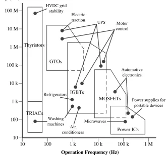
with these applications, are illustrated in Figure 2.1. However, the scope of work in this
thesis is limited to power transmission and distribution applications, i.e. 100 kVA and
above, and, as such, the following discussion will be in the context of this particular
application field.
In this Chapter, the power grid is first discussed, in order to provide the relevant
background information for this work, as well as outlining the expected future trends
of the grid. Next, the power electronics circuits that are required within the power
grid are discussed, along with the semiconductor devices that are used in these circuits.
carbide (SiC). The fundamental properties of SiC are discussed, to illustrate its advantages
offered over other semiconductor materials. In addition, some of its shortcomings and the
corresponding material challenges still being faced by researchers are presented. Finally,
a review of the current status of SiC power devices is undertaken.
100 M 10 M 1 M 100 k 10 k 1 k 100 10
10 100 1 k 10 k 100 k 1 M
Capacity (VA)
Operation Frequency (Hz)
TRIACs GTOs IGBTs MOSFETs Power ICs HVDC grid stability Thyristors Electric traction Refrigerators Washing machines Air conditioners Automotive electronics
Power supplies for portable devices
UPS Motor
control
[image:36.595.181.511.254.562.2]Microwaves
Figure 2.1: Applications of power electronics.
2.1
The Power Grid
The conventional power grid typically consists of three separate parts: generation,
end-user. The generators, which are typically large units installed in strategic locations for
operation with respect to the grid, are designed so as to produce relatively low voltages;
as such, the generated power undergoes a series of voltage transformations to increase the
voltage for efficient power transmission. The transmission system, which can be
consid-ered the backbone of the entire power system, allows power to be transferred from the
large generation plants to large consumption centres as well as other sub-transmission and
distribution systems. At the distribution end, the voltage is stepped back down to lower
voltages, for economic and safe power distribution to the end user, who is conventionally
considered as being a passive customer and does not contribute to the management of the
system in any way. In this Section, each of these subcomponents of the power grid are
discussed.
2.1.1
Power Generation
For many years, the conventional power grid has predominantly relied on the burning of
CO2 emitting fossil fuels for power generation, and continues to do so. However, with a
diminishing fossil fuel supply, not to mention the drive to drastically reduce global CO2
emissions as outlined in the Kyoto Protocol [5], it has become crucial that we look at
employing other resources for our electricity needs. Moreover, as the global population is
forecast to increase by around 25% between now and 2050 [6], it is logical to expect that
the level of our electricity demand will also increase. This problem is further compounded
by the increasing electrification in society - as an example, global sales of electric cars
are set to increase from around 2 million units in 2013 to around 10 million units in
2022 [7]. As a result, it is not hard to see why our electricity grid is in desperate need
reliable and secure in the coming decades.
For the replacement of fossil fuel power generation, renewable energy sources such as
wind, solar, wave and hydro are the most feasible options available to us. Nuclear fusion
is still a distant prospect, thus these previously mentioned sources of energy are currently
the only truly ‘clean’ forms of power generation. Encouragingly, many renewable energy
technologies today are well developed, reliable and cost competitive when compared to
conventional fuel generators. Furthermore, the cost of renewable energy technologies is
on a falling trend and is expected to fall even further as demand for the technology and
production levels increase. However, the successful large-scale integration of renewable
energy sources into the power grid is heavily dependent on power electronics, as will be
discussed in the subsequent Sections.
2.1.2
Power Transmission
As outlined in Chapter 1, the fundamental choice to make when considering a power
transmission installation is whether to employ AC or DC transmission. This decision is
based on an evaluation of transmission costs, technical considerations, and the
reliabil-ity/availability offered by the two alternatives. The overall cost of a transmission line is
comprised of two components: the capital investment required for the actual
infrastruc-ture, and costs incurred for operational requirements (i.e. losses). For similar voltage
insulation requirements, a DC line with two conductors has the same power capacity as
an AC line with three conductors of the same size. This means that, for a given power
level, a DC line requires smaller, simpler and cheaper infrastructure, and has reduced
conductor and insulator costs. Regarding the operational costs incurred, since there are
DC power transmission losses are reduced to approximately two-thirds of the comparable
AC system [8]. Furthermore, the absence of skin effect in DC lines also marginally reduces
the power losses compared to AC lines, and, lastly, dielectric losses are significantly lower
for DC transmission.
On the other hand, the cost for DC transmission terminals is significantly higher than
that for AC transmission terminals, due to the additional electrical components required
for voltage conversion. As such, it is typically the case that AC transmission is more
economical for short distances, but is more expensive for long transmission distances.
This is illustrated in Figure 2.2. It can be seen that there is a “break-even distance” that
signifies the point at which DC transmission becomes the most economical option. For
overhead lines, the break-even distance can vary from about 500 to 800 km depending on
the per unit line costs, whereas for a cable system the break-even distance is significantly
lower, approaching 50 km [8].
When considering the technical aspects of the transmission system, it becomes
ap-parent that DC transmission offers several advantages over AC transmission [8]. Firstly,
the power carrying ability of DC lines is unaffected by the transmission distance. This
isn’t the case for AC lines, the power carrying ability of whom is inversely proportional
to transmission distance due to power transfer limitations imposed by steady state and
transient stability. Secondly, whilst in an AC system reactive power control is required to
maintain a constant voltage at both ends of the line as the line loading is increased, DC
lines have no such requirement. Thirdly, in order to overcome the problems of line
charg-ing and stability limitations, line compensation is required for AC lines. Again, DC lines
have no such requirement. Fourthly, AC lines are constrained in that the interconnection
of two AC power systems requires that the line power and frequency of the two systems
Distance Costs
DC
AC
Breakeven distance
DC AC
AC line costs
AC terminal costs
[image:40.595.208.467.149.433.2]DC terminal costs DC line costs
Figure 2.2: Comparison of AC and DC transmission system costs (taken from [8]).
oscillations, fault level increases and disturbance propagation between the two systems
can occur. Due to the fast controllability of power flow in DC lines, these problems are
eliminated in DC transmission systems. Lastly, the issue of ground impedance, which is
present for AC transmission but is negligible for DC transmission, means that a DC link
can operate for extended periods using just one conductor with ground return; this is not
feasible for AC transmission.
Though the advantages of DC transmission are numerous, there are several problems
which limits its application for power transmission:
1. Expensive conversion equipment.
3. Generation of harmonics (due to the approximated DC voltage obtained from the
multi-phase converter).
4. Requirement of reactive power (for converter stations as opposed to transmission
lines).
5. Complex control system requirements.
However, significant work in the field of DC transmission has led to technological advances
aimed at overcoming the problems outlined above (with the exception of point 2). These
are:
1. Increase in the voltage/current ratings of thyristor cells.
2. Modular construction of thyristor valves.
3. Twelve-pulse converter operation, meaning reduced harmonics.
4. Use of force-commutation.
5. Application of digital electronics and fibre optics in the control of converters.
As a result of these technological advances, the reliability of DC systems has improved
while at the same time conversion costs have decreased. That said, costs still remain
rela-tively high; as such, HVDC systems are typically restricted to specialist applications such
as underground or underwater cables, long distance bulk transmission, asynchronous
con-nection of AC systems and stabilisation of power flows in interconnected power systems [8].
In addition, the use of conventional thyristor cells in the widely-used line-commutated
con-version (LCC) configuration restricts the flexibility of HVDC systems, due to the lack of
turn-off controllability. This results in poor power factors and considerable waveform
and filtering. However, the shortcomings of LCC can be eliminated by employing the
self-commutated conversion (SCC) technique, which utilises more advanced power electronics
devices with turn-on and turn-off capability. The role of power electronics in the power
grid is discussed in Section 2.2.
2.1.3
Power Distribution and the End-User
The final stage of the delivery of electricity to the end-user is the power distribution
network. This network typically consists of medium-voltage power lines in the range
1 kV to 75 kV [9], substations and pole-mounted transformers, and low-voltage
(sub-1 kV) distribution cabling, terminating at the electricity metering system of the end user.
The voltage levels used in distribution systems and their topologies vary from country
to country, and also from rural to urban areas. Due to the higher mains voltage used in
Europe when compared, for example, to the United States (230 V and 120 V respectively),
low-voltage substations typically supply a greater number of end users in Europe, as
power can be distributed over a greater distance with acceptably low power loss. In
addition, rural distribution systems typically use higher voltages than urban systems, due
to the greater distances covered by distribution power lines. As inferred previously, the
conventional power distribution system can be considered a ‘one-way system’, with power
distributed to the end-user but with no facility for power to be fed from the end-user
and back into the grid. This approach forms part of the concept of the “SmartGrid”,
2.1.4
The “SmartGrid” Concept
Though over the past few decades the development of power systems has been fairly
slow, recent years have witnessed much more significant changes to these systems. These
changes have occurred as a result of numerous factors, including the need for large-scale
integration of renewable energy sources, existing ageing assets, energy efficiency
require-ments and increasing concern regarding the security of these systems. So that security,
economy and efficiency demands are met whilst the operation of the power system
con-tinues to increase in complexity, a concept, referred to as the “SmartGrid”, has emerged.
Though there are many different views of the SmartGrid concept, a detailed definition
is given by the US Department of Energy, which defines the SmartGrid as “self healing,
enables active participation of consumers, operates resiliently against attack and
natu-ral disasters, accommodates all generation and storage options, enables introduction of
new products, services and markets, optimises asset utilisation and operates efficiently,
provides power quality for the digital economy” [10].
Central to the idea of the SmartGrid is the introduction of more advanced
informa-tion and communicainforma-tion technologies (ICTs), thus adding more intelligence to the power
grid. This has been made possible by recent developments of ICTs at acceptable costs,
which, only a few years ago, were not possible. This integration of ICTs spans the entire
hierarchy of the power grid, from smart metering systems at the end-user level, to
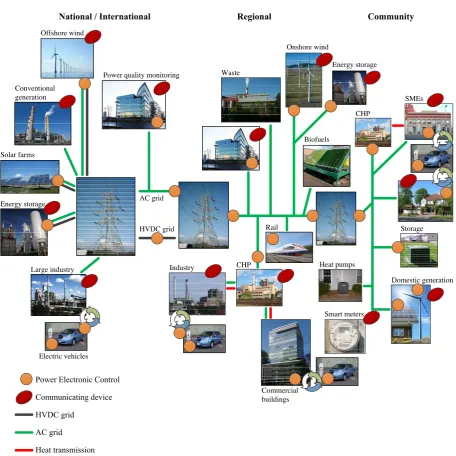
sys-tems used to control and optimise the power flow in HVDC connections. As illustrated
in Figure 2.3, in contrast to the conventional power grid system, the SmartGrid features
significant differences at the distribution and end-user levels. Though some renewable
energy units, such as large offshore wind farms, will be connected directly at the top-end
and medium-sized units will be integrated into distribution level systems. However, due
to the typically intermittent nature of energy sources such as wind and solar, and the fact
that the conventional distribution systems have not been designed to integrate a
signifi-cant number of generation units, it is crucial that intelligent management is incorporated
at this system level.
Significant changes are also underway in the once passive end-user segment, which,
conventionally, has not interacted dynamically with the power grid. Most notable is
the emergence of the previously mentioned smart meter, which wirelessly communicates
power usage and requirement data to the energy supplier, therefore regulating power with
up-to-the-minute demand. It is envisaged that, in time, the smart meter will create the
ability for electrical devices in the home to optimise their use based on a set of criteria,
and will also allow consumers to not only access usage information remotely, but also
control devices remotely; for example, to turn the heating on before the normal set time
because they are returning home early. Furthermore, the smart meter will also monitor
and control any electricity that consumers generate themselves, for example, by means of
solar panels.
Though there is little doubt that the SmartGrid methodology is the future of the power
grid, there are significant challenges that remain, but also commercial and sociological as
well as scientific and technological. Being outside the scope of this thesis, the
commer-cial and sociological challenges are not discussed herein, though are summarised in [10].
Considering the scientific and technological challenges that are being faced, these range
from understanding the interdependency between the digital and the electrical power
in-frastructures through to the integration and management of large-scale renewable energy
sources onto the grid. It is these ‘top end’ challenges that are being faced that bring us
SCC-Offshore wind
Conventional generation
Solar farms
Energy storage
Large industry
Power quality monitoring
Electric vehicles
HVDC grid AC grid
Onshore wind
Industry CHP
Smart meters Rail
Waste
Storage
Heat pumps
Domestic generation
Commercial buildings
Biofuels
CHP
[image:45.595.111.568.187.643.2]SMEs Energy storage
type voltage source converter (VSC) circuit topologies, and thus more advanced power
electronics, will be required. This is discussed in the next Section.
2.2
Power Electronics for Transmission Systems
Though it was the invention of the high-voltage mercury arc valve (which used mercury
vapour in a low pressure chamber to provide current transport and rectifying behaviour)
that initially paved the way for the development of HVDC transmission, it was the
in-troduction of solid-state power electronics, initially the thyristor, that really accelerated
the development of HVDC technology. It didn’t take long for these solid-state devices
to displace the use of mercury arc valves in new HVDC schemes across the globe, and,
as a result of substantial progress made in the ratings and reliability of thyristor valves
in the following years, the competitiveness of HVDC schemes vastly increased. More
recently, the introduction of the Insulated Gate Bipolar Transistor (IGBT) has enabled
far greater flexibility in power transmission due to its simple turn-off capability. Both of
these types of devices, and the power electronics circuits they are used in, are discussed
in this Section.
2.2.1
Requirements for Power Electronics Devices
In order for power electronics circuits to perform effectively, the semiconductor devices
used within these circuits need to be efficient (typically greater than 95% efficiency),
thus exhibiting minimal power losses. Power semiconductor devices are designed to be
operated as switches; when ‘on’, an ideal switch has zero voltage drop across it and will
carry any current imposed on it. Conversely, when ‘off’, the ideal switch will block the
![Figure 2.2: Comparison of AC and DC transmission system costs (taken from [8]).](https://thumb-us.123doks.com/thumbv2/123dok_us/9559427.460537/40.595.208.467.149.433/figure-comparison-ac-dc-transmission-costs-taken.webp)
![Table 2.1: The material properties of Si, C, 4H-SiC, 3C-SiC and GaN at 300 K [43].The mobility values shown for 4H-SiC and GaN are those along the a-axis.](https://thumb-us.123doks.com/thumbv2/123dok_us/9559427.460537/63.595.226.452.144.347/table-material-properties-mobility-values-shown-gan-axis.webp)