A Novel Implementation of Feynman Double
Gate Using Single Micro-Ring Resonator
Divya Dhawan, Mohit Khanna
Assistant Professor, Department of Electronics and Communication Engineering, PEC University of Technology,
Chandigarh, India
ME Student, Department of Electronics and Communication Engineering, PEC University of Technology, Chandigarh,
India
ABSTRACT
: U
ltrafast low-power all optical Feynman Double gate implemented using a single Silicon micro-ring resonator (MRR) has been presented in this paper, it is a notable improvement over previously available design that used two Si ring resonators for the same. The theoretical logic analysis is carried out using time domain coupled mode theory. The simulations are carried out for average pump pulse energy of 10pJ and duration 0.2ps and this design is optimized for carrying logical operations at 20Gb/s.KEYWORDS: Feynman Double gate, micro-ring resonator, time domain coupled mode theory, all-optical, low power
I. INTRODUCTION
Optical systems can bring revolutionary changes owing to low latency, high speed and virtually infinite bandwidth at such high bandwidths. Optical systems are also less susceptible to interference compared to electrical systems. Today in most of the networks logic operations are carried out using electrical logic/devices and the data is then transmitted optically, this optical to electrical conversion gives rise to high energy loss. Si-photonics has emerged as a promising candidate to circumvent these problems. On one side it offers advantages of optics i.e. high speed, parallelism and large bandwidth on other side it offers CMOS compatibility and dense integration, low weight and power. Latency can also be minimized by using Binary Decision Diagram. [1]
Conventional digital circuits inherently lose information, Landauer proved that every bit of information lost carries energy loss of kT log(2) Joules or 0.0172 eV at room temperature [2], which in itself may not seem much but this loss is only fundamental or ideal, real loss is many folds greater than it, secondly a chip contains million of logic gates on it. Hence there is a need to make circuits, thus the logic, reversible, for making them work at ultra low power. A switch is the building block of any logic circuit. Silicon MRRs are suitable for optical switching because of its compactness, advancements in fabrication.
II. RELATED WORK
The optical switching in MRRs has been proven experimentally in 1x1and 1x2 configurations [4,5] . And/Nand gates have been implemented using (1x1) MRRs only[5] . These had low switching speed ns-ms and thus the information bit rate was low few kbps. Soref and Caulfied proposed a structure having dual MRR, which used unidirectional signal propagation for cascadability hence the design required more switches. [6]. BDD based Silicon MRR is the best candidate for large scale integration, low power, low delay devices that can operate over large bandwidth.
III. RING RESONATOR THEORY
Si micro ring resonator employed in this design consists of a couple of straight waveguide and a circular waveguide as shown in fig.1. It has two input ports (input and add) and two output ports (through and drop). It uses two types of lasers at input port one responsible for pumping, being more powerful than the other and other is probe input, and these can be thought of as input to a digital gate, coupling effect takes place in the region which is close to both the straight and circular waveguide, thereby a part of the input enters into the ring.
Fig1.: Ring resonator
The intensity of photons at different ports is governed by the nature of Interference, which can be constructive or destructive depending on the optical path. If the probe frequency is in resonance with ring then it goes to drop port otherwise it goes to the through port. For the ring resonator to work as Xor gate a logic complementary to probe input is applied at the add port and at resonance the output is high at through port, for the circuit to work as switch no need to give input at add port. The optical path is variable as a phenomenon called two photon absorption, TPA, takes place and it is linked to the refractive index of the ring, hence the refractive index is changed, so does the optical path length. Hence for a given input (probe) the output is controlled or switched by the pump laser.
IV. MATHEMATICAL MODEL
The switching of add-drop MRR is modelled using time-domain coupled mode theory[11]. Ring is a source of energy, a lumped oscillator such that |A|2 is equal to the power of oscillator. The time rate of change in ring energy depends upon pump frequency, resonant frequency, pump input decay rate due to absorption and decay caused by coupling to external waveguide and coupling to input waveguide. Resonant frequency in itself is changed linearly because of change in refractive index caused by change in free carrier concentration by two photons absorption (TPA) and non-linearly because of the presence of high energy field inside the ring. Similarly decay rate is also increased significantly because of the increased carrier concentration. The mathematical equation governing the field inside ring is written below.[8-11]
( ) =− − − ∆ ( ) − ∆ ( ) ( ) (1)
−[ − ∆ ( )− ∆ ( )] ( )−[ + ] ( )− 2 ( )
Where is the amplitude of energy field inside the ring, square of which is equal to the energy, is the frequency of pump input is the initial resonance frequency corresponding to wavelengths of 1550.50nm and 1550.70nm respectively, ∆ is the change in resonance frequency due to linear effects, ∆ is the change in resonance frequency caused by non linear effects, =9.53*109 [11]is the initial rate of decay due to absorption,
∆ ∆ being the linear and non linear change in the rate of decay due to absorption respectively, are the respective decay due to energy lost in external coupling with input and drop waveguides. The non linear changes in resonant frequency and decay rate are described by equations (2) and (3) respectively. [11]
∆ =− | | (2) ∆ = | |
Where c is the speed of light in m/s, = 0.45∗10 / is the kerr coefficient, = 3.48is the refractive index Veff is the effective volume with area 450nm x 250nm radius 5µm and area / areaeff =0.82, Veff is more than
original ring volume on account of distortion in field near the corners, =0.79 / is the TPA coefficient.
TPA leads to generation in free carrier, which is counteracted by increase in recombination of free carriers governed by equation (4) [10]
( )
=∆ | |
ħ V −
( )
(4)
Where N(t) is the free carrier concentration per m3 at time t, ħ is the energy of photon of pump laser, = 15 [10] is the recombination time of free carrier, V is the volume of the ring.
The presence of free carrier is translated into change in refractive index and increased rate of absorption as stated in equation (5) and equation (6) [11]
∆ = ∆ + ∆ =− [8.8∗10 ∆ + 8.5∗10 (∆ ) . ] (5)
Where ∆ is the change in refractive index due to change in electron and hole concentrations, ∆ and ∆
respectively both ∆ and ∆ are equal to N(t) as the free carriers are generated solely by pump input. [11]
∆ = ∆ + ∆ = 8.5∗10 ∆ + 6∗10 ∆ (6)
Where ∆ is the change in absorption rate in per cm.
Change in refractive index and absorption coefficient are reflected back proportionately in the change in resonance frequency and rate of decay as shown by equation (7) and equation(8) [11]
∆ =− Γ∆ (7) ∆ =Γ ∆
2 (8)
Where ∆ is the linear change in resonance frequency and ∆ is the linear change in rate of decay,
Γ isaconstantwhosevalueis0.92.[11]
In order to find ( ) have been divided time into slots of 0.01fs and assumed that all parameters used in the above equations remain same within a time slot and all the change happens at the end of a time slot, which is a valid assumption as the length of time slot is million order magnitude lesser than the on time of pump laser. The advantage of this approach is there is no need to solve the differential equations for pump field and free carrier concentration as integration is changed to summation by this quantization of time. Subsequent values of pump field, are stored in an array and resonant frequency and rate of decay etc, equation (2) to (8), are updated every 0.01fs to be put in equation (1) till the pump laser is On.
The normalized energy field at through and drop ports of ring resonator can be defined it terms of coupling coefficient, phase after one revolution inside ring, and round trip loss as stated in equations (9) and equation (10). Though at first glance it may look simple to solve hence ring resonator is easy to model, the parameters on the right hand side are simply not known as such, but these are dependent on the strength of input itself, hence need to be derived from the equations (1) to (8) but at the time pump is off, in which all switching takes place, all the non linear effects cease to matter as they are proportional to fourth power of input field hence negligible due to weak probe laser, now phase varies due to reduction in refractive index caused by free carriers, these free carriers also increase the round trip loss. There is an exponential decay in free carrier concentration with time constant being 15ps which is reflected back in phase [13]
= −
∗
1− ∗ ∗ (9) =
− ∗
/ /
1− ∗ ∗ (10) t= (1-k2)0.5 (11)
Where k1 =k2= -0.3i, k1 and k2 are the coupling coeffient, / are the loss incurred in covering one and half revolutions inside ring respectively at loss of 1.2db/mm[12]. As the device is symmetrical values of are interchanged when the probe is applied from add port instead of input port.
The relation between phase and refractive index is described as: ∆ =∆ . 2 . / (12)
The wavelengths of probe inputs are different ie 1568.70nm [5] and 1532.70nm respectively, hence phase will be different
In the absence of pump field equation(4) is reduced to : N(t)= N0 e-t/τ (13)
N(t) is used to calculate both phase and ∆ using equations (5) and (6) . ∆ and intensity absorption coefficient 1.2db/mm is then used to calculate round trip loss . These values are then put in equations (9) and (10) to calculate through and drop energy fields.
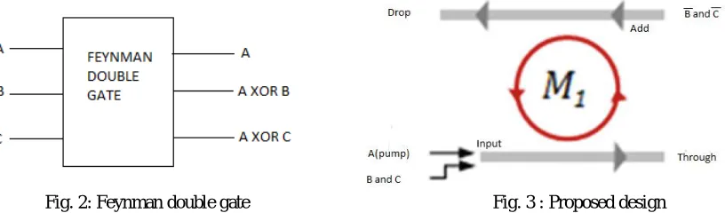
V. FEYNMAN DOUBLE GATE
Feynman double gate is a reversible gate with the outputs A, A xor B and A xor C, A is taken as impulse pump input while B and C are the probe inputs to two different ring resonators as shown in fig. 2. The vacuum wavelengths of both B and C were taken to be same[10] . In this paper the vacuum wavelengths of two probe inputs are different, as shown in fig. 6, hence the same may be given as input to one ring resonator instead of two and while in previous case probe and pump are separated from each other on the account of different wavelengths, same can be done in this case with two probe inputs. B, A and C are given through the input port while the inputs B’ and C’ are given through the add port as shown in fig.3. While generally the wavelength of probe input is close to the resonant wavelength of ring resonator and the free carrier generation due to pump causes the two to coincide, In this case the two input probes are in resonance with ring resonator in the absence of pump input and when the pump input is given the two probes are in the resonance with ring resonator no more. In other words owing to the choice of wavelengths the roles of drop and through ports are reversed in our design, which means in the absence of pump probe will go to drop port everything else being the same.
Fig. 2: Feynman double gate Fig. 3 : Proposed design
When the pump input is turned on it induces a large number of free careers, as high as the order of 1018 in the ring, and because of this the refractive index of resonator is reduced due to the plasma dispersion effect, absorption coefficient is also increased unpleasantly. So the efficiency is reduced as lesser number of photons is received at output ports. With reduction in refractive index the optical path is reduced and so does the resonant wavelength. In the absence of pump input these free carriers decay exponentially with time constant being 15ps and this time constant impose ultimate restriction on the speed of operation. All the non linear effects cease to matter once the probe input is turned off. Hence there is no need to numerically integrate and simulate the dynamic equations of ring resonator, equations (1) to (8) ; the analysis thereon is carried out using a much simpler set of linear equations which do not need to incorporate the techniques of numerical integration equation (9) onwards. Hence modeling of ring resonator becomes a way easier than it would have been. All one need to do is to incorporate the free carrier generated by pump and rate of absorption of both photons and free carriers in calculations.
A lot of research is being done towards reduction of free carrier lifetime, though the response time is faster than conventional electrical circuits, the virtually infinite bandwidth present because of operating at wavelengths of the order of 1micrometer can only be reaped fully if carrier recombination lifetime is reduced.
VI. RESULTS AND DISCUSSIONS
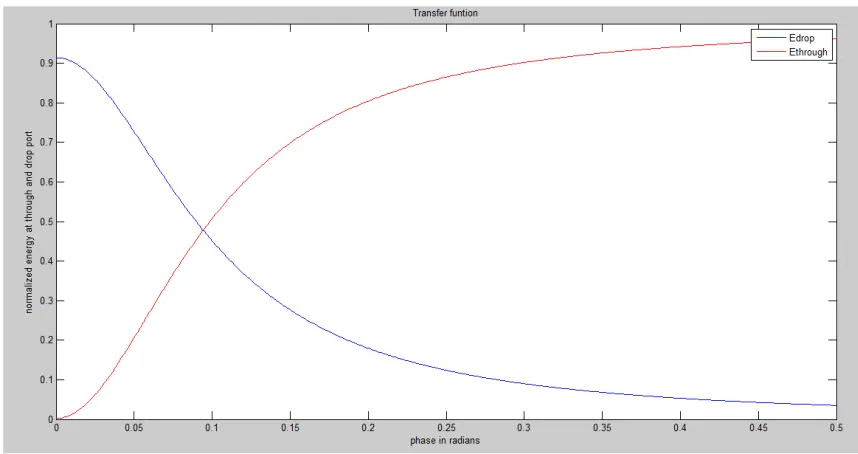
Square of energy field is equivalent to energy received at output ports. The relation between output energy and phase is graphically represented in fig. 4 after taking into account the equations (9) – (12). As shown in the figure at a phase of 0.091 radians the drop port and through port have the same output levels, it is at these points that the output is said to be switched with high on one side and low on other side. Though the output levels are periodic i.e. the graph copies itself
there any benefit available at larger phase(difference). From fig. 4 it is inferred that on/off ratio is more at 0 phase difference i.e. in the absence of pump field but the absolute value of high is more in the presence of pump input.
Fig. 4: Variation of output energy with phase at coupling coefficient=0.3 with loss =1.2db/mm
Fig. 5 shows the variation of output energy with coupling coefficient. It is required that output is high at drop port when the input wavelength is equal to the resonance wavelength of ring resonator hence value of k less than 0.1 are not permissible, ring resonator works fine for value of coupling coefficient ranging from 0.1 to 0.2 but the switching contrast is low, so generally the ring resonator is operated at coupling coefficients greater than 0.2 and switching contrast, on/off ratio, is high for these values as shown in fig.5
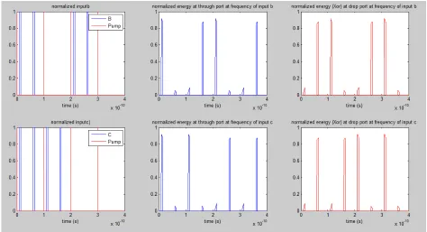
On applying the pump input of power both electron and hole concentrations are found to be to be 2*1018 /cm3 and ∆ to be 28/cm, pump input wavelength 1.555nm for 0.2ps, the results are consistent with [12] the observed value of 14.6/cm and free carrier concentration of 5*1017 on applying pump power of 1.5 mW. Fig. 6 shows the normalized energy of pump and probe inputs at add and input port and the normalized values observed at drop and through ports. These outputs are analogous to voltage levels in electronic or electrical circuits.
Fig. 6: Simulations of Feynman Double Gate
When probe is applied just after the pump input, then 1 is observed at through port however if probe is applied when the pump had not been on for more than 50ps the strength of free carrier inside ring is not enough to divert the probe to through port hence it passes through drop port. The probe inputs applied at add and input ports are complementary to each other. ON/OFF ratio is also found to be greater than 10dB from fig.6.
VII. CONCLUSION
Feynman double gate using single MRR has been presented, which offers improvement in terms of area as previously available design uses 2 MRRs for the same simulations of the proposed design are carried out in Matlab and the design is shown to perform correctly at a frequency of 20 Gb/s and uses very low pump power with low response time of 50 ps. Losses will also be reduced owing to the reduction in number of resonators. The On-Off ratio is also high (10dB).
REFERENCES
1. Xu, Q., Soref, R.: Reconfigurable optical directed-logic circuits using microresonator-based optical switches. Opt. Exp. 19, 5244–5259 (2011)
2. Landauer, R.: Irreversibility and heat generation in the computing process. IBM J. Res. Dev. 5, 183–191 (1961)
3. Bogaerts, W., De Heyn, P., Van Vaerenbergh, T., De Vos, K., Selvaraja, S.K., Claes, T., Dumon, P., Bienstman, P., Van Thourhout, D., Baets,
R.: Silicon microring resonators. Laser Photon. Rev. 6, 47–73 (2012)
4. Almeida, V.R., Barrios, C.A., Panepucci, R.R., Lipson, M.: All-optical control of light on a silicon chip. Nature 431, 1081–1084 (2004)
5. Xu, Q., Lipson, M.: All-optical logic based on silicon micro-ring resonators. Opt. Exp. 15, 924–929 (2007)
6. Caulfield, H.J., Soref, R.A.: Universal reconfigurable optical logic with silicon-on-insulator resonant structures. Photonics Nanostruct. 5, 14–20
(2007)
7. Sethi, P., Roy, S.: All-optical ultrafast adder/subtractor and MUX/DEMUX circuits with silicon microring resonators. In: Dolev, S., Oltean, M.
8. Sethi, P., Roy, S.: All-optical ultrafast switching in 2 × 2 silicon microring resonators and its application to reconfigurable DEMUX/MUX and reversible logic gates. IEEE J. Lightw. Technol. 32, 2173–2180 (2014)
9. Sethi, P., Roy, S.: Ultrafast all-optical flip-flops, simultaneous comparator-decoder and reconfigurable logic unit with silicon microring resonator switches. IEEE J. Sel. Top. Quantum. Electron. 20, 118–125 (2014)
10. Sethi, P., Roy, S.: Ultrafast All-Optical Reversible Peres and Feynman-Double Logic Gates with Silicon Microring Resonators. , LNCS 8911,
pp. 21–36, 2014. Springer-Verlag Berlin Heidelberg (2014)
11. C. Manolatou and M. Lipson, “All-optical silicon modulators based on carrier injection by two-photon absorption,” J. Lightw. Technol., vol. 24,
no. 3, pp. 1433–1439, Mar. (2006)
12. Tanay Chattopachyay “All-optical reversible network design using microring resonator”. IEEE IEEE J. Sel. Top. Quantum. Electron. VOL 51
(2015)
13. “Ring resonator: Theory and modelling”. The compendium, springer (2007)
BIOGRAPHY
Mrs. Divya Dhawan is currently working as Asst. Professor in ECE Department of PEC University of Technology Chandigarh, India. She has a teaching experience of nearly 18 years. She is a member of IEEE, ISTE, and IEI. Her research interests include Optical Communication, Photonics Systems and Digital system design.