353
Integrated Fine and Coarse Grain Clock Controller
1
T.Joby Titus, 2Dr.V.Vijayakumari, 3V.S.Sanjana Devi
1
Assistant Professor (Sr.Gr.) , 2 Professor, 3Assistant Professor 1
Dept of Electronics and Communication Engineering ,2
Dept of Computer Science and Engineering 1
Sri Ramakrishna Institute of Technology, Coimbatore-10 2
Er Perumal Manimekalai College of Engineering,Hosur 3
Dept of Electrical and Electronics Engineering 3
Sri Krishna College of Technology, Coimbatore-42.
Abstract—The clock network power is the major contributor of dynamic power and it limits the usage of integrated chips for low power applications. The previous researchers have suggested clock gating technique as it limits the switching activity by disabling the clock nodes. This clock gating is implemented with individual clock controller and modified further as fine grain clock controller. In our proposed work an architecture level modification to integrate fine and coarse grain controller to limit switching and leakage power for active and idle states.The data activity, clock distribution path and logic block are the design factor for architecture level with a small increase in circuit space.The fine grain clock is activated for individual clock nodes and the coarse grain clock activates the subsequent clock stages. The integration of clock controller identifies the shortest path and uses multiple clock nodes. This proposed model is analysed using Tanner Eda with benchmark circuit of 16-bit logic adder in nm-CMOS configuration. Around 24% of reduction in dynamic power and 20% reduction in leakage power with reduced delay is obtained in comparison with conventional clock controller network.
Index Terms—Fine grain clock, Coarse grain clock, buffer sizing, clock skew, multiple power modes, polarity assignment, multiphase.
Introduction
Technology scaling in CMOS technology leads to gradual increase in clock frequency and chip capability as a result, power dissipation becomes a complex design issue. Power consumption in CMOS technology circuits is classified in to two categories as dynamic power consumption and run time power consumption in sleep mode. The dynamic power consumption is mainly due to clock network switching, redundant clock transitions and activity of finite state machines. The basic methodology for reducing these parametric changes is by using clock gating. With increase in clock gating techniques the area utilization of clock controller network itself contributes to overall dynamic power.Sleep mode power depends on the supply voltage and current through the transistor. Power gating technique in CMOS processor technology is an effective technique to reduce leakage power.The run time power consumption in scaled devices of CMOS technology is limited by modifying the data path and providing supply voltage variation. For synchronous circuits, for every clock cycle there is a larger capacitance impact and clock signal is the major source of dynamic power consumption.The construction of clock network impacts on two concepts i.e) number of fan-out bits from logic network, number of flip flop and sharing of flip flops for common clock signal.To reduce the poweroverhead due to
effective fan out of bits it leads to increase in area overhead. The flip-flop grouping is followed based on the probability of correlation of flip-flop toggling. Many cases of clock gating techniques are applied to the first level of gate activation and the majority of redundant activation occurs only at subsequent stages. It is better to consider the clock activation at each nodes to avoid redundant clock activation and as the clock signal drives the flip-flop at far end an optimized data bus specific clock controller to be provided.[1]Abdulkadir Utku Diril, et.al, uses a voltage level conversion to obtain the threshold voltage for CMOS gates and this voltage conversion uses a level shifter with dual voltage supply. The interchange on high voltage gates with low voltage gates uses a variable threshold voltage for reduced power consumption. [2] Chao-Chyun, Chen et.al analyses the multiphase outputs of the divider in the DLL to obtain variable-phase clock to improve the performance of the device by a factor π/n, where n = delay line.
354
proposed that traditional clock gating is improved by an optimized bus specific clock gating with XOR gates and this reduces the flip-flop activity. A centralized fine grain architectural level clock gating is used for obtaining low power mode and in this mode no additional computational is used for generating clock enable signal. [5]Mohsen Riahi Alam, et.al, explains that the data path of finite state machine is controlled to obtain reduced power consumption.A fine grained approach is used for assigning polarity along with buffer size variation. Deokjin Joo, et.al [6]focussed on shortest path route and assign variable polarity to the multiple nodes.A multi-step switching scheme is used for achieving nanosecond-transient and fine-grained on- chip voltage regulation with digital low dropout regulator (DLDO).Fan Yang et.al [7] suggested that an adaptive control and multistep switching scheme provides a fast transient switching. Modification in finite state machine leads to disabling the logic network associated with it. The power and performance of the device depends on the type of controller used. To reduce the overall power consumption a variable clock controller is utilized at different levels of logic nodes. The superscalar processor is composed of large number of logic blocks and all these blocks are not activated for the same clock pulse. In the architecture level itself the designer can assign clock gating techniques to enable or disable the blocks at RTL design phase. The proposed design phase is analysed in architecture level for data path variation and circuit level for clock signal variation. The previous clock gating techniques are reviewed in section-II and the toggling rate of data variations with clock power is analysed. The clock gating conditions enables/disables the logic blocks irrespective of data variations. The unnecessary switching activity in logic network leads to increase in total power consumption of the device and considering these limitations a lowpower mode can be obtained by providing variation in clock activity, switching of data activity and the number of transistor used.The key contribution of our paper is by introducing an integrated fine grain and coarse grained clock controller. The fine grain controller manages the individual clock nodes to avoid undesirable timing, area and power overhead. This method provides a centralized approach to provide a coarse grained controller by combining fine grain clock nodes. The finite state machine involved in data path is activated based on the controller output.This paper is organized as follows, the previous clock gating techniques are explained in section II. In section III, the idea and model parameters required for proposed data is analysed. Section IV explains the proposed methodology. The experimental analysis for grained clock node controller for different nm
configurations are analysed and the results are presented in section V. This paper is concluded in section VI.
II. Previous Clock gating Methods
355
two or more clock cycles then the stability condition is used [R. Fraer et.al, 2008]. For large scale design, an observable don’t care condition is used for register transfer level of clock gating. The don’t care conditions are obtained from the multiplexer, buffer and activity states and the redundant computation is avoided.
The clock source is provided around the target domain and is connected through the clock controller with variable frequency activity to obtain better power savings. In order to disable the entire logic block it is efficient to disable based on the data activity. Based on this approach the subsequent logic node power is reduced to a greater extent compared to conventional clock methods.
III. Motivation and research background
In clock distribution network with clocked loads the amount of power consumed is about one third to one half of total device power. This indicates that clock source, clock distribution path and clock activity is the major contributors in clock network. Ideally for all sequential elements the clock signal should reach at the same time and in practice due to propagation delay in clock distribution path it is varied. The difference in clock arrival time is considered as clock skew and it leads to performance degradation and achieving zero skew is a difficult task. In LiLi et.al,2013 method of fine grain controller generates an enable signal based on flip-flop state and present data input and as it depends on flip-flop state it leads to greater clock skew.
Fig-1: Flip flop out and data driven activity
A solution to minimize clock skew and to disable low active clock nodes is done with two types of controller i.e.) fine grain clock controller and coarse grain clock controller. In fine grain controller instead of XORing the individual data state and the flip-flop output it is better to consider the data activity at each clock nodes and based on these data variations the clock signal at clock nodes are utilized. The average dynamic power estimated at the clock node can be expressed as
𝑃𝑐𝑙𝑘 = 0.5
𝑉𝐷𝐷2 𝑇𝑐𝑙𝑘
𝐶𝑒𝑓𝑓
Where VDD is the supply voltage, Tclk total clock time period, Ceff is the effective capacitance at clock nodes. The data driven gating techniques can be effectively utilized by considering the small change in data activity. In fine grain controller the next state flip-flop is disabled only due to the data variations at clock nodes. Consider the data inputs as {D0, D1…Dn} and the data activity is estimated as Dn⊕ Dn-1for t state clock cycles.
For stage-1 clock node
𝐸𝑛 = {(𝐷1⊕ 𝐷2)€(𝐷3⊕ 𝐷4) … … … (𝐷𝑛 −1⊕ 𝐷𝑛)
As the data activity varies the XOR output is modified which leads to change in enable signal. The enable signal activity for each clock nodes are varied and the choice of utilizing a common clock signal is based on the coarse grain controller.
IV. Proposed model Integration of Fine grain and coarse grain controller
A. Fine grain controller in active mode
Consider a data specific bus technique to design a controller for flip flop activation. During clock controller activation the clock node is provided with a common clock signal in which the enable for clock controller is chosen from the XORed data state. For 16 bit logic node there are 216data variations and the fine grain controller generates enable signal for 16 active state. In this technique an XOR gate output combined with clock signal activates the clock using dynamic logic gate.
Fig-2: Fine grain clock with common clock activity
B. Coarse grain clock controller
In coarse grain controller the subsequent clock nodes are activated based on flip-flop controller. During the clock time period the output of flip-flop are combined, in this one of the input is output of previous state flip-flop and the other is the enable signal for previous state. The combination of XOR gate fan-out generates an enable signal, which commonly serves a set of logic blocks. This technique provides feasibility in data variation and the enable signal generated provides common idle and active time period.
356
If fine grain controller alone is used then first stage clock nodes are controlled and if a coarse grain controller is used then the subsequent clock stages are activated. This integration technique provides a greater reduction in dynamic power and leakage current of the transistor with minimized propagation delay.
V. Experimental Results
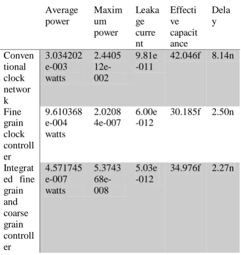
[image:4.595.43.265.263.374.2]The power and delay comparison of integrated fine and coarse grain controller with conventional method is shown in Table-1.The delay in clock activity is reduced from 8.14n to 2.50n.
Fig-3: Enable signal for clock activity
Table 1: Comparison of clock controllerswith conventional methods Average power Maxim um power Leaka ge curre nt Effecti ve capacit ance Dela y Conven tional clock networ k 3.034202 e-003 watts 2.4405 12e-002 9.81e -011
42.046f 8.14n
Fine grain clock controll er 9.610368 e-004 watts 2.0208 4e-007 6.00e -012
30.185f 2.50n
Integrat ed fine grain and coarse grain controll er 4.571745 e-007 watts 5.3743 68e-008 5.03e -012
34.976f 2.27n
VI. Conclusion
In this paper we propose to combine data activity based integration of fine grain and coarse grained controller for clock signal activity. We started with a fine grain
controller that activates the subsequent clock nodes based on random data activity.Combining different clock nodes and activating a common clock source leads to coarse grained controller. Experimental results analysed using Tanner EDA tool shows that integrated fine grain and coarse grain controller leads to a 24% reduction in dynamic power and 20% reduction in leakage power compared to conventional clock gating methods.
VII. ACKNOWLEDGEMENT
This research was supported and carried out at Department of ECE, Sri Ramakrishna Institute of Technology, Coimbatore. I would like to thank our management, Director (Academics), Principal and research supervisor for supporting us with the facility to carry out the research work.
REFERENCES
[1] Abdulkadir Utku Diril, “Voltage level shifter free design of Low power dual supply voltage CMOS circuits using dual threshold voltages,” IEEE VLSI SYSTEMS, vol. 13, no. 9, pp. 1103–1107, Sept. 2005.
[2] Chao-Chyun Chen,Jung-Yu Chang, Shen-Iuan Liu, “A DLL-Based Variable-Phase Clock Buffer,” IEEE Transactions on Circuits and Systems, vol. 54, no. 12, pp. 1072 – 1076, Dec. 2007.
[3]Ehsan Pakbaznia, “Design of a Tri-Modal Multi-Threshold CMOS Switch With Application to Data Retentive Power Gating,” IEEE VLSI SYSTEMS, vol. 20, no. 2, pp. 380–385, Feb. 2012.
[4] Li Li, Ken Choi, “Activity-DrivenFine-grained Clock Gating and Run Time Power Gating Integration,” IEEE VLSI SYSTEMS, vol. 21, no. 8, pp. 1540 – 1544, Aug. 2013.
[5] Mohsen Riahi Alam, “Power Efficient High-Level Synthesis by Centralized and Fine-Grained Clock Gating,”IEEE Computer-Aided Design of Integrated Circuits and Systems, vol. 34, no. 12, pp. 1954 – 1963, Dec. 2015.
[6] Deokjin Joo, “A Fine-Grained Clock Buffer Polarity Assignment for High-Speed and Low-Power Digital Systems,” ,”IEEE Computer-Aided Design of Integrated Circuits and Systems, vol. 33, no. 3, pp. 423 – 436, March 2014.
[7] Fan Yang, “A Nanosecond-Transient Fine-Grained Digital LDO with Multi-Step Switching Scheme and Asynchronous Adaptive Pipeline Control,” IEEE Journal of Solid-State Circuits, vol. 52, no. 9, pp. 2463 – 2473, Sept 2017.
[8] Shmuel Wimer, “Design Flow for Flip-Flop Grouping in Data-Driven Clock Gating,” IEEE VLSI SYSTEMS, vol. 22, no. 4, pp. 771 – 1544, April. 2014.
[image:4.595.41.287.425.685.2]357
[9] Jingwei Lu, “Fast Power- and Slew-Aware Gated Clock Tree Synthesis,” IEEE VLSI SYSTEMS, vol. 20, no. 11, pp. 2094–2103, Nov. 2012.