Abstract
MINEO, CHRISTOPHER ALEXANDER. Clock Tree Insertion and Verification for 3D
Integrated Circuits. (Under the direction of Dr. W. Rhett Davis)
The use of three dimensional chip fabrication technologies has emerged as a solution
to the difficulties involved with the continued scaling of bulk silicon devices. While the
technology exists, it is undervalued and underutilized largely due to the design and
verification challenges a complex 3D design presents. This work presents a clock tree
insertion and timing verification methodology for three dimensional integrated circuits
(3DIC). It has been designed in the context of and incorporated into the 3DIC design
methodology also developed within our research group. The 3DIC verification methodology
serves as an efficient means to perform all setup and hold timing checks harnessing the
power of existing commercial chip design and verification tools. A novel approach is
presented in which the multi-die design is temporarily transformed to appear as a traditional
2D design to the commercial tools for verification purposes. Various parasitic extraction
algorithms are examined, and we present a method for performing accurate 3D parasitic
extraction for timing purposes. We offer theoretical insight into the optimization of a 3D
clock tree for power savings and coupling-induced delay minimization. A practical example
of the 3DIC design and verification flow is detailed through the explanation of our research
group’s test chip, a nearly 140,000 cell 3D fast Fourier transform chip currently awaiting
Biography
Christopher Alexander Mineo was born on September 19, 1981 in Manhasset, NY.
For most of his life he has lived in northern New Jersey with loving parents Ron and Paula,
and wonderful sister Kim. Chris received the Bachelor of Engineering degree in Electrical
and Computer Engineering with a VLSI concentration from Rutgers, The State University of
New Jersey—New Brunswick in 2003. In the fall of 2003 he began the Master of Science in
Computer Engineering program at North Carolina State University in Raleigh. Shortly
thereafter, he joined the Methodologies for User-friendly System-on-a-chip Experimentation
research group under the advisement of Dr. Rhett Davis.
Since graduating from Rutgers University, Chris has worked at BAE Systems North
America in Wayne, NJ. There he primarily wrote VHDL to program FPGA’s for
communication systems. He also works at IBM in Research Triangle Park, NC. At IBM
Chris works with both the custom digital circuits VLSI teams and the timing teams on the
next generation PowerPC processor.
Chris currently works as a research assistant at NC State University on the 3DIC
project funded by DARPA. This project involves primarily the design of complex digital
systems, design tool modification and development, and design and verification methodology
Acknowledgements
I would first like to thank my parents and sister for the love and support they
continually give both on this project and everything else I am involved with. I surely could
never be where I am now without their encouragement. It is wonderful to know I can always
count on them no matter what is going on.
I certainly owe many thanks to Dr. Davis for the insight and motivation that has got
me to finish this project. He is an excellent advisor with genuine interest in all aspects of
chip design and enthusiasm that cannot help but rub off on those around him. He always
seems to be able to make himself available and takes a real interest in each of his students to
make sure they succeed.
I also thank Dr. Franzon for his interest in the areas of this work, for serving on my
thesis committee, and for being an advisor on the 3DIC research project. I thank Dr.
Rotenberg for also serving on my committee and looking at my work from a computer
architecture point of view. Thanks to Dr. Steer for also being a faculty advisor on the 3DIC
project and helping with the background knowledge about parasitic extraction.
I appreciate the help Hao Hua and Ambarish Sule, other members of my research
group, were always willing to give. They are also working on the 3DIC project; Hao helped
me a lot with the specifics of the 3DIC design flow and with making some of the flow charts.
Ambarish designed the FFT used as a test chip to demonstrate all of our work, and helped me
out also with the figures below and the specifics of the architecture of the test chip that I
I also definitely thank my friends for the support (and distraction) they provide. First,
my girlfriend Lana is always there to relax with, work with, and always seems to be proud of
me. My buddies from home are always ready to stop what they are doing when I come home
and are only a phone call away, thanks so much to Ryan, Mike, Kris, and the rest of you
guys. Thanks to Brandon, Kory, Dave, Samson and my friends around here for helping me
Table of Contents
List of Tables ... vi
List of Figures... vii
Chapter 1: Introduction ...1
Chapter 2: 3DIC Design Process ...7
2.1 3DIC Technology... 7
2.2 3DIC Design and Verification Flow ... 9
2.2.1 Inputs to the 3DIC Design and Verification Flow ... 9
2.2.2 Partitioning... 10
2.2.3 Via Insertion... 11
2.2.4 Floorplanning and Physical Design ... 12
2.2.5 Verification ... 14
2.3 Clock Tree Insertion ... 18
Chapter 3: 3DIC Timing Verification Methodology ...29
3.1 Inputs to the 3DIC Timing Verification Flow ... 29
3.2 SPEF File Merging ... 30
3.3 Circuit Simulation of Clock Tree... 34
3.4 Static Timing Verification ... 43
3.5 Timing Closure ... 48
Chapter 4: Parasitic Extraction ...50
4.1 RC Extraction... 50
4.2 Parasitic Extraction Algorithms... 51
4.3 Electromagnetic Field Solvers and Capacitance Matrices... 52
4.4 3D Extraction versus 2.5D Extraction ... 55
Chapter 5: Results and Analysis ...63
5.1 FFT Architecture... 63
5.2 Static Timing versus Circuit Simulation... 68
Chapter 6: Conclusion...73
List of Tables
List of Figures
Figure 1-1: The Four Valid Timing Arcs of an AND Gate ... 3
Figure 2-1: Cross Section of a 3D Process ... 7
Figure 2-2: 3DIC Design and Verification Flow ... 9
Figure 2-3: 3D Chain of Three Inverters ... 11
Figure 2-4: Cross Section of a 3D Via... 12
Figure 2-5: 3DIC Verification Flow ... 14
Figure 2-6: 3DIC Timing Verification Flow ... 17
Figure 2-7: Ideal Zero-Skew 8 Level H-Clock Tree with Buffers... 19
Figure 2-8: Pi Model of Interconnect with Driver and Load ... 20
Figure 2-9: Pi Model of Interconnect with Coupling Capacitors ... 23
Figure 2-10: FFT Timing Uncertainty Plot... 26
Figure 2-11: FFT Clock Power Consumption Plot ... 27
Figure 3-1: Simulation Based Timing Verification Flow ... 34
Figure 3-2: Static Timing Based Timing Verification Flow... 43
Figure 4-1: Capacitance Matrix Formulation [6]... 53
Figure 4-2: Example Net 1 in First Encounter... 55
Figure 4-3: Example Net 1 in Q3D... 56
Figure 4-4: Example Net 2 in First Encounter... 57
Figure 4-5: Example Net 2 in Q3D... 58
Figure 4-6: Inter-tier Via Modeled in Q3D... 59
Figure 4-7: Shielded Inter-tier Via Modeled in Q3D... 61
Figure 4-8: Winograd FFT Architecture... 62
Figure 5-1: FFT Tier A Clock Tree ... 64
Figure 5-2: FFT Tier B Clock Tree... 66
Chapter 1: Introduction
We are rapidly approaching the 35 nm technology mark where one billion transistors
will physically fit on a single traditional bulk silicon chip. The current trend of device
scaling in bulk silicon CMOS processes has been progressing for 30 years, but in order to
continue building high performance circuits, threshold voltages would have to shrink
proportionately. This is beginning to cause a number of other significant problems
previously unseen, including leakage current, noise susceptibility, and yield due to
manufacturing defects. Experts believe that if the trend of increasing chip complexity known
as Moore’s Law is to continue, the industry will undoubtedly turn to alternatives to classic
bulk silicon technology. Well known possibilities include double gate fully-depleted
silicon-on-insulator (SOI) devices, fin-FET transistors, and the topic of this paper, three-dimensional
SOI processes [1]. The 3D SOI processes are particularly appealing because they allow for
chips of higher complexity while also addressing the problem of increased wire delays in
today’s chips.
In modern technologies, interconnect in circuits has overtaken gate delay as the
dominant source of path delay in complex chips. Multiple dies (also known as tiers) in a
single integrated circuit (IC) package not only allow designers to fit more transistors—hence
additional functionality—in a chip, but also drastically reduce average interconnect length
between circuits. Shorter wires, and in turn smaller wiring capacitances, offer both
performance and power saving advantages over traditional two-dimensional processes. Our
research group tested these claims by fabricating a chip in such a 3D process, overcoming
multiple challenges in the process. One important challenge, on which this work is focused,
and verification methodology for three dimensional integrated circuits (3DIC) immediately
with the available tools. However, today’s design tools are based on 2D chip design. An
entire suite of design software is needed to bring a new chip to fruition in a competitive
amount of time; and we, like industrial chip designers, do not have the time to wait for
commercial tool vendors to address our needs.
Aside from the lack of 3D design features in tools, every chip designer is aware of the
shortcomings of modern design tools with how fast the industry is evolving. Many modern
day tools are the result of large companies acquiring a number of smaller companies and
doing their best to integrate all the tools together. As technologies evolve, the requirements
of design tools change and the electronic design automation (EDA) industry is often reluctant
to make the enormous time and financial commitment involved with redesigning a tool from
the ground up. Chip designers that have strict deadlines to meet certainly cannot rely on
EDA companies to release new tools or fixes for every difficulty they encounter. The result
is designers and in-house support teams regularly incorporating their own design
methodologies and custom EDA tool fixes into a standard design flow. Such is the case with
the recent introduction of three-dimensional IC manufacturing processes. In a 3DIC process,
separate dies are combined and interconnected within a single package. The dies are
fabricated on different wafers, quite possibly in different foundries. The wafers are brought
together, ground very thin, aligned, and stacked. Inter-tier vias are created, which much like
traditional vias, are vertical segments that connect metal layers. The inter-tier vias, however,
connect a metal layer in one die with a metal layer in another die and are significantly larger
than traditional vias. These inter-tier vias will be discussed in detail in chapter 2 and are
any of this, especially inter-tier connections. The problem that will be addressed here is how
to use commercially available EDA tools to reach timing closure on a complex synthesized
3DIC. A solution is presented in the form of a primarily manual methodology with complex
steps being automated in a variety of ways.
A
Y B
A B Y 0 0 0 0 1 0 1 0 0 1 1 1
A B0 Y0
A B0 Y0
A B1 Y
A B1 Y
A0 B Y0
A0 B Y0
A1 B Y
A1 B Y
1 2
3 4
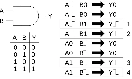
Figure 1-1: The Four Valid Timing Arcs of an AND Gate
We consider a chip to have met timing closure after examining each chip-level timing
arc in the entire chip, and ensuring that each arc passes all setup and all hold timing tests.
The simplest set of timing arcs is seen in figure 1-1. Any two-input, one-output gate has the
potential to have 8 timing arcs as shown. A timing arc is a specific path of signal
propagation from a transitioning input to a transitioning output while all other inputs are set
to constant values. An AND gate, for example, has just four valid timing arcs, since the ones
not boxed do not have transitioning outputs. In this chip-level work, the timing arc concept
is abstracted to the chip level, where each path can contain multiple gates. In this case the
starting point of a timing arc can be either the primary input to a chip or the output of a
register, and the ending point of a timing arc can be either the input of a downstream register
or the primary output of a chip. Therefore, in order to close timing we must check each
violations. This process will account for clock skew and assume a certain frequency of
operation.
The timing verification methodology for a 2D chip is well known and available EDA
tools are well-equipped to handle such a task. For single clock designs with no clock-gating,
cycle stealing or other timing tricks, the verification process is nearly pushbutton and is
mostly handled under the covers of complex tools. In essence, RTL for a design is often
coded in a hardware development language, synthesized into a gate-level netlist, then placed
and routed using a physical design tool. Once the design is placed and routed, we can extract
parasitic resistive and capacitive (and at times inductive) values for all interconnections
between gates. By combining this information with standard cell library files, a static timing
analysis program can efficiently determine delays for each timing arc and determine if it
meets timing. Timing tools can efficiently be used in a variety of ways and can even be run
in batches to make a large number of calculations through the use of custom scripts. The
amount of timing data that can be efficiently obtained using static timing tools is enormous
when compared to circuit simulation based tools such as Spice, at the expense of a small
degree of accuracy.
There are a number of difficulties that a designer faces in this timing verification
process when beginning to use a new technology, especially a 3D process. First of all,
designing the chip is more complex. Our research group has formalized the 3DIC design
flow; the major difficulty being that 3DIC’s have not yet been addressed by vendor tools.
We have created a design and verification methodology that resembles a 2D design flow to
such an extent that existing tools can be used. My contribution has been the clock tree
very important modifications to a 2D flow, mostly revolving around the fact that all tools
have to treat each tier as an unrelated chip. This creates complications in timing verification,
because many timing arcs travel between tiers and we need some way to time the design as a
whole. That is the main issue being addressed here, is how to reach timing closure in the
presence of a 3DIC design flow developed around traditional 2DIC design tools. A novel
approach is presented to accomplish this by operating on intermediate files to make a 3D
stack of interconnected dies appear as if it is a normal 2D chip to the design tools. Timing is
analyzed using two independent approaches, circuit simulation and static timing.
First we will discuss the 3DIC technology and examine the 3DIC design methodology
and 3DIC timing verification methodology on a high level, from a user’s perspective. For
simplicity we will discuss the design flow mainly as it pertains to the inputs to the timing
verification flow, and present a novel approach to optimizing the clock tree. In designing the
clock tree, we will examine how a specific 3D configuration can optimize the clock tree for
power consumption and delay uncertainty. Next we will dive into the timing verification
methodology again, but in deeper detail; all along the differences and similarities between the
proposed flow and the standard 2D flow will be addressed. Chapter 4 then serves to validate
the flow’s accuracy; there will be a discussion of RC parasitics in general and how they were
computed in this study. Finally, the results section will provide the reader with data showing
how closely the simulation versus static timing data match, and see how this methodology is
applied in a practical example. The 3DIC design flow and the 3DIC timing verification flow
work were used in the April 2005 submission of our research group’s FFT chip using the
MIT Lincoln Labs 3D FDSOI technology. The reasons for success will be investigated and
points of the 3DIC clock tree insertion and timing verification methodology will be
Chapter 2: 3DIC Design Process
2.1 3DIC Technology
It is important to go into some detail about a typical 3DIC fabrication process. The
design methodologies in the following discussions were created such that they would be
portable to any 3D process available with little or no modification. However, they were
designed with the MIT Lincoln Labs 180 nm FDSOI 3D process in mind because that is
currently the only set of 3DIC design rules available to universities, which we used to
fabricate the test chip to be discussed later. The essentials of this process are outlined by a
cross-sectional diagram in figure 2-1.
TIER C BURIED OXIDE
TIER B BURIED OXIDE
TIER A BURIED OXIDE
M1C
Patterned Back-Metal
M2C
M3C
WAFER BOND
WAFER BOND VIA BC
M1B
M3B
M3A
M1A M2B
M2A
VIA AB
The MITLL process uses three tiers, with three metal layers on each. It uses two different
types of inter-tier vias, a VIA AB and a VIA BC. VIA AB electrically connects metal layer 3
in tier A to metal layer 3 in tier B. VIA BC electrically connects metal layer 3 in tier C with
metal layer 1 in tier B. After all tiers have been fabricated, first the bottom tier, tier A, is laid
down. The next tier, tier B is then inverted so the devices are face down. This is a SOI
process, so all transistors exist on islands of silicon in a buried oxide. The buried oxide is
then ground thin, essentially to transparency. Using fabrication equipment the tier B wafer is
aligned and bonded on top of the tier A wafer. Then the locations for the instances of VIA
AB are identified, etched, and filled. After that, the same process is performed for tier C; it is
inverted, ground, aligned, bonded, and all VIA BC’s are created. On the back of the highest
tier is a back-metal layer. This serves primarily to contact ground vias for heat dissipation,
Synthesis Result (Normal Netlist)
Physical Design: CTS, Place & Route Partition
Partitioned Netlist (Merged Verilog
Netlist)
Via Insertion
Floorplan
pass
Merged 3D Layout and Extracted GDSII
Database.
DEF files & SPEF files with
Parasitic RC
Timing, Thermal & Physical Verification
fail
Tier Specific Netlist
Thermal/Signal Vias, Placed Module/IO Pad, Power Planning
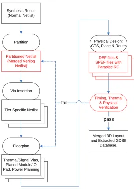
Figure 2-2: 3DIC Design and Verification Flow
2.2 3DIC Design and Verification Flow
2.2.1 Inputs to the 3DIC Design and Verification Flow
The 3DIC design and verification flow is a complex methodology, so at this point we
will outline the important details to understand the complications that a 3D technology
causes, specifically making note of the information we have to work with when verifying that
the chip meets timing. The overall 3DIC physical design flow developed by our research
group is shown at the highest level in figure 2-2. The timing verification methodology was
of flow charts will be referred to for clarity. Steps shown in red are of particular importance
and will be discussed again in detail as we continue. Steps shown in blue are complex steps
that have been automated through a variety of scripting languages. We represent user action
with an oval and important files as rectangles. Figure 2-2 shows the timing verification steps
in red. This methodology begins with completed and logically verified RTL Verilog code
that has been synthesized successfully into a Verilog netlist, just as would be done when
creating a 2D chip. This Verilog netlist is the “Synthesis Result” shown as the starting point
in the figure.
2.2.2 Partitioning
Now that we have a netlist for the entire design, we must decide which modules and
which gates will be placed on which tier. This process is shown as the “Partition” step. The
design is partitioned into tiers such that the average wire length across the design is
minimized. The quantity of vias is also a concern, because the inter-tier vias are rather large
and using too many of them results in a waste of chip area. We can see this in figure 2-3, a
3D rendering to scale of a chain of three CMOS inverters. The NMOS are shown in green
and the PMOS are shown in brown. The large orange and yellow structures contacted by the
grey metal 3 strips are the inter-tier vias. The input to the chain is on the bottom tier, and the
output on the highest tier. The partitioning step is largely automated with python scripts,
which write out an important file hereafter referred to as the merged Verilog netlist. This file
is shown in red in figure 2-2 because we use it as an input to the timing verification flow.
This file is written out for both verification purposes and use in other design steps. It
describes the entire design, but is broken up into hierarchy showing which gates are on which
Figure 2-3: 3D Chain of Three Inverters
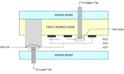
2.2.3 Via Insertion
In the “Via Insertion” stage, inter-tier via cells are instantiated in the design wherever
there is a connection between any two tiers designated by the newly added hierarchy.
Simultaneously, the single netlist is broken up into separate netlists, one file for each tier of
the design. Figure 2-4 shows the details of an inter-tier via and what is involved with
inserting one. The fabrication information for each tier must be submitted to the foundry
VIA Land cell on the lower tier. A VIA Cut consists of a via layer surrounded by and
partially overlapping a ring of metal. The electrical connection is made by the via going
through the metal ring. The VIA Land consists of a landing pad of metal and a via layer
coming down to meet it; each has associated design rules. The specifics of inter-tier via
creation are irrelevant here, but it is important to recognize that in order to fabricate one 3D
via there must exist an instance of VIA Cut in the layout for one tier, and in the tier
immediately below it, in the same location, an instance of VIA Land. This means that in the
“Via Insertion” step, we must split the merged Verilog netlist into separate files, and in order
to instantiate a via, one VIA Cut must be instantiated in one file and a corresponding VIA
Land in another file.
TIER X BURIED OXIDE
M1X M2X
M3X
WAFER BOND
WAFER BOND
To Higher Tier
To Lower Tier
VIA Land
VIA Cut
Figure 2-4: Cross Section of a 3D Via
2.2.4 Floorplanning and Physical Design
Referring back to figure 2-2, we can continue with the “Floorplan” stage. This step is
complicated because in three dimensions there are more options. We also have the added
task of inserting inter-tier vias that exist for the specific purpose of channeling heat out of
this stack of insulators. After the “Floorplan” step we are ready to let the EDA tools work
with the design more. There now exists a separate netlist for each tier of the chip, complete
with floorplanning decisions. Even the VIA Land and VIA Cut cells that have been
instantiated are treated by the 2D design tools the same as any other instantiated cell with
ports and abstracted circuit elements inside. Therefore, a physical design tool such as
Cadence’s First Encounter can handle the exact placement and routing of the cells in each
tier-specific netlist individually. In each tier we first place the cells, and then use First
Encounter’s built in clock tree synthesis tool to insert clock tree buffers into the layout. First
Encounter then routes each tier individually, and we can manually connect the clock tree
from each tier together. Upon completion, First Encounter writes out a set of important files
for each tier. For each tier a design exchange format (DEF) file and a standard parasitics
exchange format (SPEF) file is created. The DEF file is a type of netlist that includes
connectivity and floorplanning information; it completely describes the layout of the tier.
The SPEF file is also a netlist, but describes each segment of interconnect in detail. It gives
all resistive and capacitive values associated with each net. A complete description of a net
in a SPEF file lists each pin on each standard cell to which the net is connected. Then, it
breaks each straight jog of metal in the net into an RC Pi model. Each time a path turns at
90° a new segment with a Pi model is listed, whether the path is changing directions in the
same metal layer or turning out of its plane through a via. There is an option in First
Encounter to have the SPEF file include coupling capacitors separately in the parasitics,
work is complete, and what remains are several verification flows and intricacies to prepare
the design for submission to the foundry. We will next explore the verification step, which
includes the 3DIC timing verification methodology.
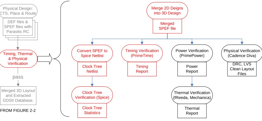
Merge 2D Deigns into 3D Design
Merged SPEF file
Convert SPEF to Spice Netlist
Timing Verification (PrimeTime)
Power Verification (PrimePower) DEF files &
SPEF files with Parasitic RC
pass
Merged 3D Layout and Extracted GDSII Database. Physical Design: CTS, Place & Route
Timing, Thermal & Physical Verification Thermal Verification (fReeda, Mechanica) Clock Tree Netlist Timing Report Power Report Thermal Report Clock Tree Verification (Spice) Clock Tree Statistics Physical Verification (Cadence Diva) DRC, LVS Clean Layout Files
FROM FIGURE 2-2
Figure 2-5: 3DIC Verification Flow
2.2.5 Verification
Figure 2-5 gives an overview of the verification methodology for a 3DIC. We can
start with the physical verification steps. Design rule checking (DRC) is fairly similar to that
of a 2D chip; when the DRC deck of design rules is being written it must include all design
rules having to do with the insertion of inter-tier vias, in addition to those having to do with
device construction and wiring for the specific process. Layout versus schematic (LVS)
checking is slightly more complicated because we need to physically compare the
preliminary schematic of the design with the completed layout to make sure there are no
short circuits or other mistakes that would result in the layout and schematic not having all
identical devices and connections. This means that we have to make the 3D chip appear as a
2D design to the LVS tool. This is done by again using the merged Verilog netlist from
2D netlist is critical to both the LVS step mentioned here and as a starting point for the
timing verification flow. The common idea behind the physical verification methodology is
that we have to analyze the design as a whole, not the tiers individually. In order to do this
we must make the complete 3D design appear as a 2D design to the EDA tools. We apply
this idea to the timing verification as well.
In figure 2-5, we can now look at the parts shown in red, which specifically represent
the timing verification flow. The power and thermal verification are handled by separately
using other Synopsys tools and tools developed within the university, which is outside the
scope of this paper. The timing verification is performed in two somewhat independent ways
in order to validate each other, as can be seen in figure 2-6. One way is by obtaining clock
tree data such as skew, slew rate, and insertion delay through Spice circuit simulations. The
same tasks that were performed by the simulations are then performed using static timing
analysis with Synopsys’ PrimeTime tool. We then use PrimeTime to time the design as a
whole to check for timing violations; paths of particular interest can then be reanalyzed using
Spice at the user’s discretion. Looking again at figure 2-6, we start with the SPEF files that
we have extracted for each tier. Through the use of a custom Perl script, spefmerger, we can
combine these files into one SPEF file such that it can be used to annotate the merged
Verilog netlist with parasitics. We use this merged SPEF file to perform a number of tasks.
First, a custom Perl script, spef2spice, has been written specifically to convert a SPEF file
into a Spice netlist. This way we can perform circuit simulations of interesting or important
parts of a design. Having a hierarchical Verilog netlist and a compatible SPEF file allows us
to use static timing to time however much of the design we desire. In this verification flow,
the whole design. It is the steps involved with this timing verification on which we focus in
chapter 3, by explaining figures 3-1 and 3-2 in detail.
The objective is to design a 3D chip using commercially available 2D EDA tools as
much as possible, and deviating from the 2D complex chip design flow as little as possible.
The idea is to produce the simplest method possible to successfully create a 3DIC
immediately. The design and verification processes for a 3D chip has now been summarized,
but before proceeding to the verification portion it is necessary to review how timing closure
is met for a 2D chip. The process is normally totally completed using a static timing analysis
tool. One complete Verilog netlist exists, and after placement and routing, there exists a
SPEF file with which the Verilog netlist can be back-annotated to include parasitics. The
clock tree is inserted using a physical design tool; some timing constraints are given to the
tool and it does its best to produce a clock tree that will meet the specification. The static
timer is fed some technology information about metal layers and parasitics, and files that
describe the timing properties of each cell in the standard cell library. All of this information
can be included in files adhering to the Synopsys Liberty (LIB) and Open Library Exchange
Format (LEF) standards. A member of a timing team then reads into the timing tool a LIB
file and a LEF file, a Verilog netlist, and the corresponding SPEF file. After that, more
timing constraints will need to be set, the complexity of which often varies with the
complexity of the design being timed. The user would typically specify the periods and duty
cycles of all clocks, arrival times of valid signals at primary inputs, and any special situations
such as false paths at the very least. In general the number of clocks in the design and how
often they interact with each other dictates how much effort setting up these assertions
they give the specified number of worst slack setup and worst slack hold timing arcs. If the
worst slack is positive, then timing is generally considered closed. Timing tools usually have
the option to receive their commands in the context of a language such as TCL (tool
command language), so if any more specific or other data besides worst slack paths is desired
it can be calculated and post-processed. The largest complication between this method and
what is available in a 3D flow is that this 2D flow needs to be modified to accommodate the
fact that the only available parasitic information is in three separate files. The next chapter
will now go into the details of the 3D timing verification flow.
Tier Specific SPEF File With Parasitic RC Tier Specific
SPEF File With Parasitic RC Tier Specific
SPEF File With Parasitic RC
Merged SPEF File Spice
Library Netlist File Merged Verilog Netlist
Determine Whether Timing Closure
Achieved
Clock Tree Statistics Timing Report
Merge Tier Specific SPEF Files
Perform Circuit Simulation of
Clock Tree
Perform Static Timing Analysis
Timing Data, Layout Files ready for GDSII
Extraction
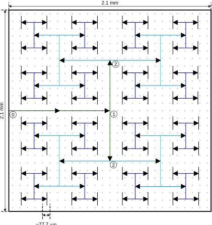
2.3 Clock Tree Insertion
We have outlined how to verify a clock tree that has been routed to multiple tiers, and
it is important to discuss how to build the optimal clock tree. Depending on application, we
will consider optimal to be either the clock tree with the lowest timing uncertainty, or the
clock tree which consumes the least power. The FFT clock tree was designed using First
Encounter’s clock tree synthesis tool almost entirely, but if it was necessary some custom
design work could have improved its performance; it makes a good example for the
following analysis. For the FFT a timing constraint file imposed some requirements on the
tool which it attempted to adhere to while inserting clock buffers and routing the clock tree.
The clock tree insertion tool automatically routes the clock tree to a pad on the perimeter of
the chip, so by inserting a clock tree automatically on each tier and forcing the clock pad to
be in the same spot on each tier, we can easily manually connect the signal on the tiers and
have a satisfactory clock tree. This method requires little designer effort, and as will be
shown, is not a bad one.
Many of the issues a designer faces when creating a 3D clock tree are the same as the
ones faced when inserting a 2D clock tree. For this reason, we will make some assumptions
that force us to concentrate on the optimizations that apply just to the 3D aspect of clock tree
synthesis. We will use the number of clock sinks in the FFT design and the dimensions of
each tier; we will assume the clock sinks are distributed uniformly across three tiers, and are
evenly spaced within each tier. Modern clock tree synthesis tools generally use some form of
an H-tree clock tree, so we will also assume an H-tree in order to analyze a tool-generated
clock tree. To distribute the clock we will assume an ideal zero-skew H-tree of eight levels;
an eight level H-tree in the described situation means that each last stage buffer has a fan-out
optimal designs generally have a fan-out of 4. This clock tree is shown in figure 2-7, and we
will assume that it is replicated in each of the tiers. The different levels of the clock tree are
shown in different colors, starting in dark green and fading to dark blue then black. This
leaves the question, of when we should branch into the third dimension. At this time we will
discuss both how to buffer the clock tree and where to place the inter-tier vias based on the
most critical objective.
2.1 mm
2.1 m
m
~77.7 µm
1 0
2
We will attempt to optimize the clock tree based on timing uncertainty and power
consumption by placing the inter-tier vias in an optimal location. For this analysis we can
say that we have the choice of branching to 3D at point 0 (at the perimeter), point 1 (after
level 1—between the dark green and green routes), point 2 (after level 2—between the green
and turquoise routes), and so on, as labeled in figure 2-7. In this clock tree, we have 9
choices of where to branch, points 0-8 although only 0-2 are labeled for simplicity. In this
decision there will be trade-offs because different branch points require different lengths of
wire and different quantities of inter-tier vias. For example, if we choose to branch at point 2
then we say levels 1 and 2 (the dark green and green routes) will only exist in the center tier
but all other routes exist in all tiers. However, if this was the case then we need 4 inter-tier
vias to distribute the clock, one going up and one going down at each point labeled 2.
Similarly, if we branch at point 0 then the entire clock tree is replicated on each tier but we
need only 2 inter-tier vias. However, first we will address another issue concerning wire
length, how to insert the buffers shown in figure 2-7. Too many buffers will result in a
drastic waste of power, but too few results in long insertion delays and large slew rates.
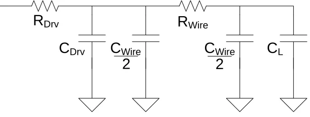
R
DrvC
DrvC
WireC
WireC
LR
Wire2
2
Figure 2-8: Pi Model of Interconnect with Driver and Load
In general we can determine the optimal length of interconnect between repeaters
line is represented as a Pi model with capacitance CWire and resistance RWire. The line is
driven by a gate with output resistance RDrv and output capacitance CDrv. The line is loaded
with another gate, the input capacitance of which is seen by the line as CL. According to the
Elmore Delay, the propagation delay along this RC network is td = 0.69·τ, where τ is the sum
of RC time constants along the path of interest as dictated by this timing approximation.
This model is shown in figure 2-8, and the calculation of τ for this network is:
(
)
⎟ ⎠ ⎞ ⎜ ⎝ ⎛ + + + ⎟ ⎠ ⎞ ⎜ ⎝ ⎛ += Wire L
Wire Drv Wire Drv Drv C C R R C C R 2 2
τ (1)
Certain substitutions can be made so that τ is a function of more general process parameters.
The substitutions include:
s r
R d
Drv = rd = driver resistance (Ω·μm)
s c
CDrv =3 o co = driver output capacitance (fF/μm) s
c
CL =3 g cg = load gate capacitance (fF/μm)
L r
RWire = w rw = wire resistance (Ω/μm)
L c
CWire = w cw = wire capacitance (fF/μm)
The driver resistance is for a micron of transistor width, assuming the resistance is due to the
one device in the gate that is on during a given transition. The s is microns of transistor
width, assuming minimum length, so RDrv is inversely proportional to device width. The
driver resistance can be found via a circuit simulation of an inverter. From the VDS vs. ID
curve we can find the instantaneous output resistance when VDS = VDD and when VDS =
VDD/2 and average the two. The driver output capacitance is directly proportional to device
width, and is dependent on the drains of all devices. We will assume that PMOS devices will
be sized twice as large as NMOS, which is where the coefficient of 3 comes from. The
an ideal current source forcing current into the drain while the source is grounded. The
simulation can measure VDS and subtract IDS from the ideal current source. This gives
enough information to use
dt dV C
I = to find the capacitance. The gate capacitance is found
in a similar way to the driver output capacitance, except by grounding the source and drain to
keep the device in cutoff while forcing current into the gate. The parasitic resistance and
capacitance of the wire vary with L, the length of wire being considered. The values are
generally obtained from the foundry-provided information about the technology. The
resistance of each metal layer is expressed as a sheet resistance in Ω/□. The capacitance can
be found by using the provided area and fringing capacitances. We assume minimum width
wires. Making the described substitutions into (1) and performing some expansion yields
(2): ⎥ ⎦ ⎤ ⎢ ⎣ ⎡ ⎟ ⎠ ⎞ ⎜ ⎝ ⎛ + + ⎟ ⎠ ⎞ ⎜ ⎝ ⎛ + + ⎟ ⎠ ⎞ ⎜ ⎝ ⎛ +
= c s
k L c k L r s c k L c s r k L c s c s r
k d w g w w g
w o d 3 2 1 3 2 1 2 1 3
τ (2)
The only difference, however, is that we substitute in k L
instead of just L, where k is the
number of repeaters that exist along the length of wire, L. This is because we really have a
collection of smaller wire segments separated by k buffers. We also multiply the entire
expression by k, which is the equivalent of adding up all of the τ’s for the entire line.
Minimizing τ will effectively minimize the delay along the line, and k is the parameter that
we are looking to vary to perform this optimization. Therefore, in (3) we take the partial
derivative of τ with respect to k, and set the result equal to zero to find the minimum τ.
(
)
02 1 3 2 2 = − + = ∂ ∂ k L c r c c r
k d o g w w
τ
In (4) the expression is rearranged into the form that gives the optimal number of repeaters to
insert in a length of wire, L.
(
)
w w g o doptimal r c
c c r k
L = +
⎟ ⎠ ⎞ ⎜ ⎝ ⎛ 6 (4)
It is important to note that in taking the derivative, s dropped out of the relationship. The
repeaters inserted will have to be sized considering delay, power, and slew rate, yet the
number of buffers that should be inserted is dependent upon process parameters and the
length of wire being buffered. This value should be taken as a guide when inserting buffers,
but cannot be followed literally first because the number of buffers to insert is very discrete,
but also because nets have different branches and fan-outs. Nevertheless, this provides a
good starting point, one that was used in figure 2-7.
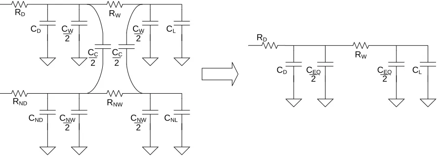
RD
CD CW CW CL
RW
CC CC
2
2 2 2
RND
CND CNW CNW CNL
RNW
2 2
RD
CD CEQ CEQ CL
RW
2 2
Figure 2-9: Pi Model of Interconnect with Coupling Capacitors
The simple model we have used so far, however, is inadequate to proceed with. For
the reasons to be described in the RC extraction chapter, we need to consider coupling
capacitances to decide when to split to 3D. When a wire has a close neighbor, a coupling
capacitance exists between them. The activity of the neighbor line can either speed up or
switching with or against the line of interest. To model this we can convert the coupling
capacitance and the wire ground capacitance to one equivalent ground capacitance.
The left side of figure 2-9 shows a segment of interconnect similar to figure 2-8, but
with the coupling capacitances connecting it to a neighboring net with parasitics marked with
an ‘N.’ The wire capacitance and the coupling capacitance from the figure are combined into
CEQ according to (5).
(
)
CW
EQ C C
C = + 1−β , and
2 DD N V V Δ =
β (5)
In (5) ΔVN = VN2 – VN1 if VN1 is the voltage of the neighboring net when the net of interest
begins to transition and VN2 is the voltage on the neighboring net when the net of interest
reaches a switching threshold of VDD / 2. In this case, the -1 ≤ (1-β) ≤ 3, so when 1-β = 3 CEQ
will be largest and the propagation delay will be longest. When 1-β = -1 CEQ will be smallest
and the propagation delay will be the fastest [3]. Using (5) we can convert the circuit on the
left side of figure 2-9 to the one on the right side for easier analysis. We will write the
Elmore Delay equation for the circuit on the right side of figure 2-9 two times, once for when
CEQ is at a maximum and once for when it is at a minimum. Subtracting these two values
and diving by two will give us the timing uncertainty in a segment of interconnect due to
coupling capacitances, assuming we have no knowledge of the activity on the neighboring
line.
Equations (6) and (7) show the maximum and minimum propagation delays that can
result from the circuit on the right side of figure 2-9.
(
)
⎥ ⎦ ⎤ ⎢ ⎣ ⎡ ⎟ ⎠ ⎞ ⎜ ⎝ ⎛ + + + + ⎟ ⎠ ⎞ ⎜ ⎝ ⎛ + += W C L
W D C W D D d C C C R R C C C R t 2 3 2 3 69 . 0
(
)
⎥ ⎦ ⎤ ⎢ ⎣ ⎡ ⎟ ⎠ ⎞ ⎜ ⎝ ⎛ − + + + ⎟ ⎠ ⎞ ⎜ ⎝ ⎛ + −= W C L
W D C W D D d C C C R R C C C R t 2 2 69 . 0
(min) (7)
All of the variables in (6) and (7) are calculated as described earlier, with the exception of CC
which was determined using an electromagnetic fields solver and assumed to vary directly
with wire length. However, that would be assuming that there is a neighboring net coupling
to the net of interest for its entire length. This is overly pessimistic so steps can be taken to
calculate the routing congestion of the design. The routing congestion calculated as an
percentage of occupied g-cell tracks after detail routing should be used as a multiplier to the
simulated coupling capacitance. From this information we can calculate the timing
uncertainty due to coupling capacitance in (8).
2
(min) (max)
inty d d
uncerta
t t
t =± − (8)
The parasitic data for a 3D via is available from the simulations to be discussed in chapter 4.
Using this we can model a 3D via the same was as we modeled the interconnect in figure 2-9,
and also calculate the timing uncertainty introduced by each inter-tier via using this method.
Because splitting the clock tree and distributing it to 3D at different points results in different
wire lengths and different numbers of inter-tier vias, splitting to 3D at different points results
in different amounts of total timing uncertainty in the clock tree. We can add together all of
the uncertainties to find a total timing uncertainty, and this would be a good value to
optimize, but we cannot take this value too literally. First of all, accurate values of rd, co, cg,
rw, cw, and cc are difficult to obtain. Next, there is not necessarily a register-register data path
between each set of storage elements. Furthermore, even if there is a register-register path
timing uncertainty when branching to 3D at each possible point, we can draw some important
conclusions.
FFT Timing Uncertainty
0 0.1 0.2 0.3 0.4 0.5 0.6 0.7 0.8 0.9 1
0 2 4 6 8
Clock Tree Levels Before Split to 3D Proportion
of Max Uncertainty
Figure 2-10: FFT Timing Uncertainty Plot
Using the described method to calculate timing uncertainty due to coupling
capacitance, we can obtain the data in figure 2-10. Since the timing uncertainty due to
coupling capacitance on wiring is much greater than that due to coupling capacitance on 3D
vias, the graph shows that in our case it is most beneficial to split to three dimensions as
close to the clock sinks as possible. The most useful information to draw from figure 2-10 is
reduce the uncertainty by less than 10%. If the clock tree is split at any place other than at
the perimeter, point 0, significant designer effort will be required. This analysis shows that
there is significant benefit to customizing the clock tree, but a lot of designer effort would
likely be required to achieve this benefit. In addition to the designer effort, the landing pad
for a 3D via is 25 μm2, so there could be very significant area increases; splitting at point 8
adds 256 3D vias to the design. The decision of where to split to 3D depends on the amount
of slack in the timing and area budgets, and the amount of designer effort that can be
afforded. We will now also examine how the power consumption varies with the split point.
FFT Clock Power Consumption
0 0.1 0.2 0.3 0.4 0.5 0.6 0.7 0.8 0.9 1
0 2 4 6 8
Clock Tree Levels Before Split to 3D Proportion
of Max Power
The clock net is one of the most power hungry nets in a chip, because it is typically
very large and switches on every cycle. The equation to calculate the power consumed by a
net is 2 0 1
2 1
→ = V fCα
P DD . If we are trying to optimize where to split to 3D, we cannot
control the supply voltage, operating frequency, or probability of a 0→1 transition.
Therefore, we control the capacitance on the net only, so the power consumed is directly
proportional to the total capacitance on the net. By the same rationale as the timing
uncertainty calculations, we can calculate the total power consumed by the clock tree for
each of the possible locations we could choose to split to 3D. Such a plot is shown in figure
2-11. We see that branching into three dimensions close to the clock sinks also helps to
conserve power, again because the 3D vias have less capacitance than the interconnect.
There is also a similar trend regarding how much designer effort and added area is needed to
Chapter 3: 3DIC Timing Verification Methodology
The design flow laid out so far proves to have been a success because as far as the
tools are concerned, we are designing several independent 2D chips. It is through user
interaction and processing steps in between EDA tool steps that the seemingly independent
chips are made compatible with one another and can be interconnected to form a 3DIC. Like
the physical design DRC / LVS verification, we intend to verify timing by treating the design
as a whole and making the multi-tier design appear as a 2D chip.
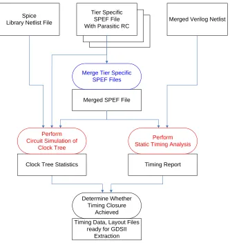
3.1 Inputs to the 3DIC Timing Verification Flow
This section begins the detailed explanation of the timing verification flow shown in
figure 2-6. The figure shows the input data and output data, along with the necessary tool
executions. Besides the theoretical clock tree analysis, this was my main contribution to the
3DIC design and verification methodology. To begin timing verification, there are five
essential inputs that must be prepared. These are shown on the top row of figure 2-6, the
high level diagram of the timing verification flow. From the design flow, we need the
tier-specific SPEF files (there are three in this case), the merged Verilog netlist, and the Spice
library netlist file. The Spice library netlist file is normally used only by those working on
the standard cell library specifically, and contains a Spice netlist for each cell that is in the
design. Continuing with figure 2-6, the first actual step in the timing verification process is
to merge the tier-specific SPEF files. This step is in blue because it has been automated and
will be discussed shortly. With the aforementioned inputs and the merged SPEF file, we can
then calculate timing data via two independent paths, the static timing analysis path, and a
circuit simulation path. We will use the similarity in results between these two methods to
each of them in greater detail. After all timing reports and such have been generated, we can
determine whether the chip meets timing, or if we need to iterate back through part of the
design process.
3.2 SPEF File Merging
Merging the tier-specific SPEF files into a single SPEF file is an important task but
has been automated with the spefmerger. The script can take up to one hour for a design
with 140,000 cells, but heavily depends on the complexity of the design and what parasitics
exactly are being extracted. To run the code, one must execute the script with four command
line arguments. A path to the SPEF file for each tier (three in our case) and a name for the
design as a whole must be supplied. When completed, and used to back-annotate the merged
Verilog netlist with parasitic information, we can once again make a 3D design appear as a
2D design so that we can operate on it with EDA tools. Theoretically, the spefmerger is
fairly simple. We first take the SPEF file from each tier and concatenate them together
section by section into one file. We must take care to change all net and instance names such
that there is no name aliasing, and then remove the 3D vias and insert propagate segments in
their place to maintain the electrical connection. However, there are a number of
complications. For the reasons to be discussed, the spefmerger is specific to the MITLL 3D
FDSOI technology and the 3DIC design flow developed by our research group. The timing
verification flow, however, is structured such that the spefmerger can easily be modified or
replaced to accommodate a slightly different 3D process or different design flow without
upsetting the surrounding steps.
Primarily, the spefmerger must follow every single convention assumed by the code
and instances are changed during floorplanning and merging, because of tier placement,
position in a re-powering tree, if connected to a pad cell, etc. Also, there are naming
consistency problems that arise between Verilog and SPEF files which are normally taken
care of under the covers of other tools but become our responsibility here. There are certain
characters that sometimes must be escaped in each type of file because they have special
meanings, and hierarchy delimiting characters in one type of file can create an illegal net
name in the other. There is quite a bit of translation in the names alone to associate the
parasitics with the correct net.
We also must be selective about which nets from the individual tiers we include in the
merged SPEF file for fear of duplicating nets, such as those connected to pins that were
instantiated for the sole purpose of creating re-powering trees. Also having to do with name
mapping and aliasing problems is the way that the SPEF file refers to nets and instances. At
the top of the file there is the “NAME_MAP” section. Here every instance and net in the
design is given a number; from that point on the net or instance is referred to by that number
preceded by an asterisk (*). Therefore, we need to also avoid net/instance number aliasing
when merging the files. Also, when the parasitics of a net are described, that one net number
is broken down into many subnets. For example, net *1 may be broken down into *1:1, *1:2,
*1:3, etc., all of which are connected by different resistances to maintain the same electrical
connections as *1, and all of which could have different capacitances. If an inter-tier via
connects net *1 in tier A with, for example, net *5 in tier B, we would have first offset *5 in
tier B so that the net is referred to as *(5+x) where x is the total number of nets and instances
in tier A so that *5 in tier B could not alias with *5 in tier A. Then we would have found the
are the same net. Then we must offset all of the subnet assignments in the tier B portion of
the net so that they do not share any subnet numbers with the tier A portion of the net, or else
we would be shorting together parts of the net and lose parasitics that we should be
accounting for.
After the naming conventions are settled, there is the task of actually removing the
3D via and joining the nets that were joined by the 3D via. First we need to identify a 3D
via, which we cannot do solely using net names. If we were to identify which nets in one tier
were connected to a net in another tier only by some sort of suffix added to the net name, we
would not know which specific subnet to make the connection at. Instead we need to use net
name suffixes and standard cell library names. In our research group’s standard cell library,
all 3D via cells (and only 3D via cells) had names starting with ‘V’ so that was used to
identify a 3D via cell and the specific net subnets it was connected to. Then we use the net
names to know which net in another tier is connected to the current net. Unfortunately this is
one reason that this code is specific to a standard cell library, albeit an easily modifiable one.
Perhaps the most obvious problem is that we need to insert a parasitic resistance and
capacitance for the 3D via. Seeing as current EDA tools have no notion of 3D vias we
certainly cannot extract the parasitics of one using design tools. Instead, we needed to
perform electromagnetic field simulations to determine the parasitics of an inter-tier via.
This was as interesting and accurate approach, which we will discuss in the RC extraction
chapter later. Assuming we can now replace the 3D via with an interconnect Pi model, how
we connect the nets from each tier, i.e. if we need to add subnets or modify existing ones,
depends on how the RC network is connected to the 3D via cell and whether there was
ability to handle coupling capacitors. For future integration of a crosstalk analysis tool into
the 3DIC verification methodology, we would need to supply a merged SPEF file that
includes coupling capacitors. While experiments have shown timing runs to be accurate with
lumped ground capacitances, this also gives the user the option to include coupling effects in
timing calculations.
The last complication with the spefmerger to be discussed here has to do with run
time. Based on the fact that it is not uncommon for SPEF files to be two million lines long or
longer, the code dealing with them is difficult to write. It must not load too much into
memory and must avoid traversing the entire file more than once or else run time would grow
too high. The code is also writing out a file that contains all the information in each
tier-specific SPEF file, which was normally between five and six million lines in our case. To
avoid the problems that were just explained and others, there were a number of complications
that result in a lot of bookkeeping during program execution. This, combined with the fact
that it was written in Perl which is an interpreted, as opposed to compiled, language already
(Merged or Tier Specific) SPEF File
Select and Format Nets of Interest List
Nets of Interest
Generate Spice Netlist
Spice Netlist
Create Test Environment
Run Spice on Circuit Segment
Raw Simulation Data
Find Skew and Slew Rates Spice
Library Netlist File
Spice Library Netlist File, Tier Specific SPEF Files
With Parasitic RC, Merged SPEF File
Determine Whether Timing Closure
Achieved Clock Tree Statistics
Perform Circuit Simulation of
Clock Tree
Spice Deck
Timing Data, Layout Files ready for GDSII
Extraction
Clock Tree Statistics FROM FIGURE 2-6
Figure 3-1: Simulation Based Timing Verification Flow
3.3 Circuit Simulation of Clock Tree
Figure 2-6 shows that at this point we can “Perform Circuit Simulations of the Clock
determine the specific performance of a placed and routed clock tree. Using a circuit
simulator we will find the skew of the clock tree, the minimum and maximum slew rates at
the clock sinks, and the insertion delay. It is first important to note that this figure makes no
mention of a clock tree in particular and that it does not specify whether we are working with
one tier individually or the design as a whole. The extraction and simulation methodology
shown in figure 3-1 will work for any circuit or segment of a circuit. It is based on
spef2spice, which when written was intended for use with clock trees but can also be used on
any other part of a circuit. It can be used to easily extract a portion of a parasitics file and
translate that to a Spice netlist for circuit simulation of any path that is of particular interest.
Furthermore, it is recommended that this flow actually be performed on the clock tree several
times independently, once for each tier and then once for the design as a whole. According
to the design methodology, the clock tree was created on each tier independently, so we
should analyze them individually first. That way we can determine whether a specific tier’s
clock tree is performing worse than the others, or if one tier’s clock tree has a particularly
long or short insertion delay that ruins the overall performance of the clock tree. Afterwards,
of course, it is necessary to analyze the clock tree as a whole. The flow will be described as
if we were running the design as a whole, but the process is the same for an individual tier.
After obtaining the merged SPEF file, we must determine which nets are to be
included in the simulation. In the case of the clock tree, the user must just create a list of the
nets that make up the clock tree. This is slightly more cumbersome for a simulation of a data
path, but it is generally easiest to create a list of the nets in a clock tree using unix
commands. A single command such as:
would very quickly write to a file called clocknets_merged each clock net listed in the SPEF
file. The second “grep” command in the line removes all of the clock buffer and inverter
instances before writing to the file; it is assumed that in the instance name instances are
differentiated from one another using I1, I2, I10, etc. Some formatting changes using a text
editor may still be necessary because later stages expect a file containing net names, one per
line, with nothing but the net name on the line.
Next we are ready to use the Spice library netlist file discussed earlier, the merged
SPEF file, and our list of nets of interest to create a Spice netlist. This step is automated by
the spef2spice Perl script mentioned earlier. Unlike the spefmerger, this code is not specific
to a particular technology or design methodology. A valid SPEF file contains all parasitics of
cell to cell interconnect and tells which subnet is connected to which pin of all standard cells
the net is connected to. Therefore, between the SPEF file and the Spice library netlist file,
we have enough information to construct a netlist. The script generates a Spice netlist that
includes each net listed in the nets of interest list. It also instantiates every standard cell with
at least one output and one input pin connected to nets in the nets of interest list, i.e. every
standard cell instance that exists between any two nets of interest. The Spice library netlist is
included with an .include statement in the Spice deck, so whenever the script needs to
instantiate a standard cell it can simply instantiate it using a .subckt Spice statement.
In order for a standard cell library to be useful, it must be characterized. This
normally consists of a large number of circuit simulations (such as Spice as in our case) on
each cell individually to find the delay of each timing arc in it over a broad range of
temperature, capacitive loading, input slew rate, etc. conditions. This information is then
calculating timing data for a large design made up of these cells. The Spice library netlist file
is normally created as an intermediate step in library characterization and would be obtained
from library developers. However, we can use it because it contains separate netlists of
every cell in the library. So long as we can reference this file from our Spice deck we can
easily instantiate cells in our Spice netlist.
Using the Spice library netlist works well for simple clock trees where the only cells
that need to be instantiated are inverters and clock buffers. In more complex trees with clock
gating, the data phase input to the clock gate may not be listed as a net of interest, in which
case that input to the gate would be labeled as a floating node and a warning message would
be printed to the screen. Such also is the case when this code is used on a data path, and
inputs to cells along the data path are nets not listed in the nets of interest list. Those inputs
also would be wired to a new net labeled as a floating node. It would then be the user’s
responsibility to edit the netlist by hand to drive those floating nodes with stimuli such that
the desired transitions along the path would result. After the netlist is created the user is
prompted with the question:
Do you want to measure skew to a pin that is common to several cells?
The user can reply “y” or “n”, the latter of which causes the run to terminate. Replying “y”
will prompt the user for the reference node. The reference node must be one of the nets
listed in the nets of interest; this net will be considered the source of the signal of which the
skew is being measured. To measure clock skew, we would enter “clk” or whichever
node/pin the voltage source driving the clock is connected to. After that, the user is
prompted for the standard cell pin to measure to. This is the name of the pin in the standard
Measure statements are then inserted to measure from the net assigned to be the reference
node, to each sink. Assuming we are analyzing a clock tree, this is effectively finding the
insertion delay. Hard coded into the script are statements that will measure rising to rising
and falling to falling transitions. Minor modifications would allow the script to work with
inverting logic paths, but this way we keep Spice from trying to measure transitions that do
not exist. When measuring insertion delay we measure from the 50% mark of the source’s
transition to the 50% mark of the sink’s transition. Measure statements are also written to
measure the rising and falling slew at each clock sink. For these inverting versus
non-inverting logic is irrelevant because the signal is measured against itself. The .measure
statements record all data over the first clock period, so long simulation times are generally
not needed.
Depending on the application, the user may choose to deviate from the default
settings in spef2spice. At the top of the code, there are three parameters the user can modify,
but they are generally not changed often so are not command line options. There exists a
variable called $use_pin_caps. The LIB file lists pin capacitances for each cell that are
included in the SPEF file separately from the wiring capacitances. Normally this variable
would be set to a 1 so that this pin capacitances from the LIB file would be included, but
when they can be ignored by setting $use_pin_caps to a 0. Like the spefmerger, this code
also can accommodate coupling capacitances. However, this poses a similar problem to
instantiating the cells. At times when coupling capacitors are used in the SPEF file a
capacitor appears between a net you intend to extract and one you do not. The net you do not
extract would not be in the simulation, and thus we would have a floating node. This