International Journal of Innovative Technology and Exploring Engineering (IJITEE) ISSN: 2278-3075, Volume-8 Issue-7 May, 2019
Abstract: This paper represents the different scan chain techniques which will be used to detect the faults in different benchmark circuits. The fault testing is done using Synopsys Tool such as Design Compiler, DFT Compiler, Prime Time and Tetramax. The prime time generates the critical path delay report which is read by Tetramax tool to insert the fault in the circuit and accordingly the faults are detected. Basically scan chain techniques are used to detect the faults in design but the advantage of these techniques is that they will also help in power reduction as represented by the analysis.
Index Terms: Scan chain, benchmark circuit, design compiler, DFT compiler, primetime, tetramax, fault detection.
I. INTRODUCTION
Testing is very important to increase the speed of device. As the technology node is decreasing, the stuck at faults detection is not sufficient to tell about the quality of product manufactured or under processing. Thus many other strategies are used together with stuck at faults such as transition faults. The testing can be done through tetramax tool. Main motive of testing is to check that our design will work according to specification or not. Consequence of noise is the main contribution for speed failure when using a technology called submicron [13]. Hence the faulty models and testing approach adapted to detect the faults in the chip. Delay defects are active and observed only by travelling the signals passing by the circuit. Most of the techniques used for delay testing are applied to combinational part of the design. Timing information will be required by the circuit for critical path and this is taken by prime time and can create a path delay report by invoking pt2tmax.tcl in the primetime tool. Many paths that cannot be sensitized, affect the performance of the circuit such that the detection of faults on them is independent of delays outside the target path. Hence, if we ignore these paths that results in a contribution to a low fault coverage of path delay. Design and synthesis for testability techniques used for improving the delay faults testability results in a high area and large number of extra primary inputs.
II. LITERATURE SURVEY
B. Pandey et al. explains that there are different types of clock gating techniques like latch free, latch based, flip flop based technique. In latch free approach there is an additional input
Revised Manuscript Received on May 10, 2019
Sakshi Sharma, Electronics and Communication Department, Jaypee
Institute of Information Technology, Sector 62, Noida, India.
Gaurav Verma, Electronics and Communication Department, Jaypee
Institute of Information Technology, Sector 62, Noida, India.
signal applied which is called „enable‟ to control clock input applied to sequential circuit. In this method RTL design contains an AND gate. There is a main disadvantage of using latch free clock gating technique is that glitch occur in this design, so second clock gating technique which is called latch based technique is used. In this technique latch is added into the design, but there is also a disadvantage of using this technique is that this will not be supportable on vertex-6 because of latches present in this technique, so next technique is used, in this technique instead of latch, flip flop is used [1]. M. P. Dev et al. shows the usage of gating techniques in sequential design [2]. J. Yadav et al. shows the application of gating techniques [3]. B. Pandeyet al. explains how clock gating techniques are implemented on FPGA [4]. D. Stroobandt et al. explains that what are benchmark circuits and generation of benchmark circuits. ISCAS provide different types of benchmark circuits like ISCAS‟85, ISCAS‟99/ITC‟99. ISCAS‟85 and ISCAS‟99 are the series of different sequential circuit and structural circuit. All benchmark circuits have some fixed flip flops, gates, lines etc [5]. X. liu, M. S. Hsiao et al. shows benchmark b01 circuit, analog and mixed signal will be tested by the standard benchmark circuit called B-01. This is the circuit which use finite state machine for comparing serial flow. As a sequential circuit contain clock, this circuit will also contain “clock” input because B-01 circuit is sequential circuit. Clock will used to control the flip flop present in design [6]. B. P. S. Tomar et al. explains that clock gating technique is used to reduce the power of the circuit which occurs due to input clock and logic switching, in this clock input is controlled by an additional input signal called enable. For testing of mixed and analog signal, benchmark circuits are used. Author used latch free technique in this paper. B01 benchmark circuit consumes some dynamic power that‟s why clock gating technique is used to reduce that power consumption. This technique used an additional signal called enable signal which is used to control the clock. Normally at 1 Hz, involvement of clock power is 1.92% of overall dynamic power. When clock gating technique is used, contribution of clock power is 38.75% of overall dynamic power. This concludes that clock gating is used for power reduction [7]. Most of the researchers talk about architectural techniques like pipelining, parallelism and clock gating techniques for power reduction [12, 14-16] but here we demonstrate that scan chain techniques can also used for power reduction. We apply muxed-D scan and clock scan techniques on different benchmark circuits and also detect transition and stuck at faults.
III. TECHNIQUES USED
Scan chain techniques are used in this paper. There are two input sources which are
Performance Analysis and Fault Detection of
Benchmark Circuits using Synopsys Tool
used by scan cell. First input is data input and another one is scan input. Input “data” is operated by circuit logic while another cell output is used to drive the second input which is called scan input. Scan chain will be formed by joining the first scan cell input to primary input and last scan cell output to the primary output. There is mechanism which is used to select the input sources in such a way that scan cell will work in two manners. First mode is normal mode and second one is shift mode. In normal mode data input is used and in shift mode scan input is used. There are two types of scan cell design which are used in this paper and these techniques are listed below:
A. Muxed – D Scan Cell
[image:2.595.312.549.200.350.2]There are different storage elements which are used by logic circuits, but mainly D flip flop is used. The main function of D flip flop is to transfer to the output which is present at input. Muxed D scan cell is used for the replacement of D storage element. Muxed-D scan consist a multiplexer and F flip flop as shown in Fig 1. Multiplexer will contain scan enable (SE) input which is used to select input as scan input (SI) and data input (DI). If scan enable (SE) input is 0 then it means scan cell will work in normal mode DI is selected. When the clock is high the then value present on data input captured by D flip flop. If scan enable input is 1 then it means scan cell will work in shifting mode and SI is selected. The data which is present in D flip flop will be shifted using SI.
Fig 1: Muxed-D scan cell and its sample waveforms Muxed-D scan cell is compatible with modern designs, this is the basic advantage of using muxed-D scan cell. Multiplexer will add in the design which will provide more delay, this is the disadvantage of using this scan cell technique.
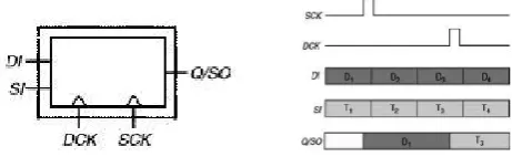
B. Clocked Scan Cell
Clocked scan technique is same as muxed D scan technique. Here also there is a replacement of D flip flop with muxed-D cell. In this there are also two input, first one is data input (DI) and second one is scan input (SI). As in muxed-D scan uses single clock for the selection of two different input, in this two independent clocks are used for the selection of Data input and scan input. First clock is data clock (DCK) and second clock is shift clock (SCK). DCK is used in normal mode to store the data which is at DI to clocked scan cell and SCK is used in shifting mode for shifting the data present in scan input to clocked scan cell as shown in Fig 2.
Fig 2: Clocked-scan cell and its sample waveforms
There is no performance degradation on the input when clocked scan techniques is used. This is the major advantage of this technique. Additional shift clock routing is necessary for using this technique, this is the major disadvantage.
IV. TESTMETHODOLOGY
[image:2.595.59.279.376.445.2]For the detection of fault in digital circuits following tools and techniques are used as shown in Fig 3. The Synopsys tools used to detect the fault in the circuit. For delay testing in digital circuits Design Compiler, DFT Max, Prime Time, Tetramax are used.
Fig 3: Test methodology
The tool which is used for the synthesis of HDL design is design compiler. Design compiler tool is used to synthesize the HDL design to gate level design. It is used for the estimating the area, power and speed. DFT compiler tool is used for the testing [10]. Scan chain is done through this tool. After that primetime tool is used for generation of path delay report [11]. This report is given to tetramax tool which is used to detect the fault in the design. Stuck at faults and transition fault models are supported by tetramax [9].
V. IMPLEMENTATIONOFBENCHMARK
CIRCUITS
There are some benchmark circuits which are used in this paper like B-01 Benchmark circuit, B-02 Benchmark circuit and B-03 Benchmark circuit. Implementation of these benchmark circuits are shown below:
A. B-01 Benchmark Circuit
Analog and mixed signal will be tested by the standard benchmark circuit called B-01. This is the circuit which will use finite state machine for comparing serial flow [5]. The schematic benchmark B-01 circuit is shown in Fig 4.
[image:2.595.315.548.640.832.2] [image:2.595.59.290.682.753.2]International Journal of Innovative Technology and Exploring Engineering (IJITEE) ISSN: 2278-3075, Volume-8 Issue-7 May, 2019
This schematic will contain four inputs and two outputs. As a sequential circuit contain clock, this circuit will also contain “clock” input because B-01 circuit is sequential circuit. Clock will used to control the flip flop present in design. “line 1” and “line 2” are single bit input whose serial flow is to be compared. There is one more input which is “reset”, it will also a single bit input. When reset input is 0 then both output will attains logic 0. Output “outp” which is the result of xoring of line 1 and line 2. Output “overflow” will attain logic according to finite state machine. The schematic which is obtained by the synthesis of B-01 design is shown in Fig 5.
Fig 5: Schematic of B-01 circuit
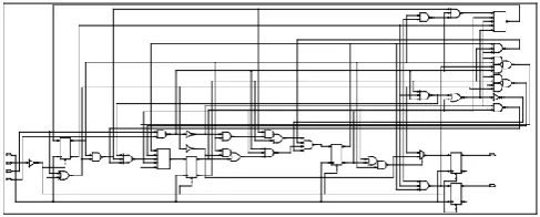
[image:3.595.307.555.121.246.2]It can be done through the synopsis tool i.e. design compiler. Design compiler will also used to estimate the power, area and time. This circuit has 49 gates, 110 lines, 2 primary inputs, 2 primary outputs and 5 flip flops. Scan chain can be inserted through the tool DFT compiler. Schematic after scan chain insertion is shown in Fig 6.
Fig 6: Schematic of B-01 circuit after scan chain insertion
B. B-02 Benchmark Circuit
[image:3.595.49.288.194.308.2]The schematic of B-02 Benchmark circuit is shown in Fig 7.
Fig 7: B-02 Benchmark Circuit
In this schematic there are 3 inputs and 1 output. Benchmark B-02 circuit is the sequential circuit so there is
one “clock is used to control the flip flop in the design, “linea” is also an input and there is one more input which is “reset”, it will also a single bit input. Output “u” is a finite state machine that recognizes BCD number. The schematic which is obtained by the synthesis of B-02 design is shown in Fig 8.
Fig 8: Schematic of B-02 circuit
It can be done through the synopsis tool i.e. design compiler. This circuit has 28 gates, 70 lines, 1 primary input, 1 primary output and 4 flip flops. Scan chain can be inserted through the tool DFT compiler. Schematic after scan chain insertion is shown in fig 9.
Fig 9: Schematic of B-02 circuit after scan chain insertion C. B-03 Benchmark Circuit
The schematic of B-03 Benchmark circuit is shown in Fig 10.
Fig 10: B-03 Benchmark Circuit
[image:3.595.308.554.334.446.2] [image:3.595.50.294.424.522.2]Fig 11: Schematic of B-03 circuit
[image:4.595.309.545.62.163.2]It can be done through the synopsis tool i.e. Design compiler. This circuit has 149 gates, 141 lines, 4 inputs, 4 outputs and 30 flip flops. Scan chain can be inserted through the tool DFT compiler. Schematic after scan chain insertion is shown in Fig 12.
Fig 12: Schematic of B-03 circuit after scan chain insertion
VI. RESULT
The result section shows the performance analysis of all that circuit which were used in this paper.
A. Power Analysis
Power is reduced after the scan chain insertion shown below:
Table 1: Analysis of power
Techniques B-01
Power (uW)
B-02 Power
(uW)
B-03 Power
(uW)
DC 22.217 15.81 137.79
Muxed-D 21.216 15.47 126.13
Clocked Scan 20.736 15.32 125.23
Benchmark B-01 circuit normally consume 22.217 uW power, after insertion of muxed-D scan cell technique power is reduced to 21.216uW and than after applying clocked scan cell technique power will reduced to 20.736uW. Benchmark B-02 circuit normally consume 15.81uW power, after insertion of muxed-D scan cell technique power is reduced to 15.47uW and than after applying clocked scan cell technique power will reduced to 15.32uW. Benchmark B-03 circuit normally consume 137.79uW power, after insertion of muxed-D scan cell technique power is reduced to 126.13uW and than after applying clocked scan cell technique power will reduced to 125.23uW.
B. Timing Analysis
[image:4.595.49.293.246.369.2]Speed of circuit is also increased by using scan chain techniques is shown in Table 2.
Table 2: Timing Analysis Technique
s
B-01 Time (ns)
B-02 Time(ns)
B-03 Time(ns)
DC 8.73 6.57 9.69
Muxed-D 7.87 5.96 9.36
Clocked Scan
6.98 4.79 8.97
Benchmark B-01 circuit normally take 8.73ns, after insertion of muxed-D scan cell technique time is reduced to 7.87ns and then after applying clocked scan cell technique time will reduced to 6.98ns. B-02 circuit normally take 6.57ns, after insertion of muxed-D scan cell technique time is reduced to 5.96ns and than after applying clocked scan cell technique time will reduced to 4.79ns. B-03 circuit normally take 9.69ns, after insertion of muxed-D scan cell technique time is reduced to 9.36ns and than after applying clocked scan cell technique time will reduced to 8.97ns.
C. Area Analysis
Comparison of area is shown in Table 3.
Table 3: Area Analysis
Techniques B-01 Area B-02 Area B-03 Area
DC 722.024 443 3050
Muxed-D
773.97 545 3470
Clocked Scan
753.52 513 3560
Area will be increased after insertion of scan chain techniques. There will always be tradeoff between area and power.
Fault detection can be done through tetramax tool. Tetramax ATPG supports ATPG as well as fault simulation for scan based path delay fault testing [8]. Tetramax supports fault model such as stuck at faults, transition fault. Path report generated by prime time is given to tetramax to detect the fault in design.
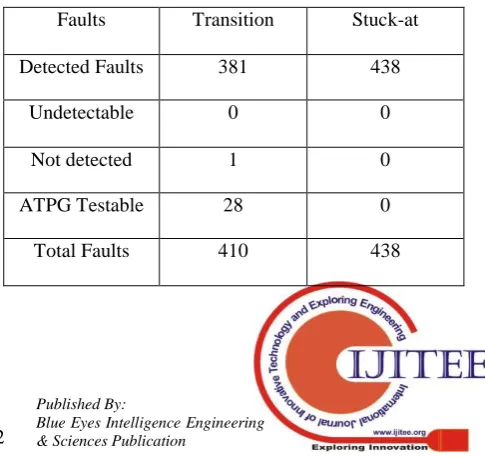
Transition and stuck at faults for B-01 circuit is shown in Table 4.
Table 4: Fault Detection for B-01 circuit
Faults Transition Stuck-at
Detected Faults 381 438
Undetectable 0 0
Not detected 1 0
ATPG Testable 28 0
[image:4.595.50.289.494.605.2] [image:4.595.303.546.607.836.2]International Journal of Innovative Technology and Exploring Engineering (IJITEE) ISSN: 2278-3075, Volume-8 Issue-7 May, 2019
Fault Coverage 93.92% 100%
Table 4 shows that there are total 410 transition faults out of which 381 faults are detected, 1 fault is not detected and there are 28 ATPG testable faults. Test coverage of the design is 92.93%, total 438 stuck at faults and all faults are detected. Test coverage of the design is 100%. Transition and stuck at faults for B-02 circuit is shown in Table 5.
Table 5: Fault Detection for B-02 circuit
Faults Transition Stuck-at
Detected Faults
390 313
Undetectable 0 0
Not detected 0 0
ATPG Testable
20 0
Total Faults 410 313
Fault Coverage
95.12% 100%
[image:5.595.55.284.428.600.2]Table 5 shows that there are total 410 transition faults out of which 390 faults are detected and 30 ATPG testable faults. Test coverage of the design is 95.12%, total 313 stuck at faults and all faults are detected. Test coverage of the design is 100%. Transition and stuck at faults for B-03 circuit is shown in Table 6.
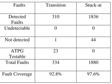
Table 6: Fault Detection for B-03 circuit
Faults Transition Stuck-at
Detected Faults
310 1836
Undetectable 0 0
Not detected 1 44
ATPG Testable
23 0
Total Faults 334 1880
Fault Coverage 92.8% 97.6%
Table 6 shows that there are total 334 transition faults out of which 310 faults are detected, 1 fault is not detected and there are 23 ATPG testable faults. Test coverage of the design is 92.8%, total 1880 stuck at faults out of which 31836 faults are detected, 44 faults are not detected. Test coverage of the design is 97.6%.
VII. CONCLUSION
This paper presents application of scan chain techniques using the synopsis tool. As testing is very important to increase speed of design or circuit, this paper explains the detection of transition and stuck at faults. However, it has been observed that the application of these techniques also helps in reduction of power. After applying scan chain
techniques, the transition and stuck at fault are detected and power reduction also takes place as observed from the analysis. So, scan chain technique is very effective in fault detection as well as reducing the power of design
.
REFERENCES
1. B. Pandey and M. Pattanaik, “Clock Gating Aware Low Power ALU Design and Implementation on FPGA”, 2nd International Conference on Network and Computer Science (ICNCS), Singapore, Vol. 2, No. 5, pp. 341-345, April 1-2, 2013. 2. M. P. Dev, D. Baghel, B. Pandey, M. Pattanaik, A. Shukla,
“Clock Gated Low Power Sequential Circuit Design”, IEEE
Conference on Information and Communication
Technologies(ICT), pp. 440-444, 11-12 April, 2013.
3. B. Pandey, J.Yadav, N. Rajoria, M. Pattanaik, “Clock Gating Based Energy Efficient ALU Design and Implementation on FPGA”, International Conference on Energy Efficient Technologies for Sustainability-(ICEETs), Nagercoil, Tamilnadu, pp. 93-97, April 10-12, 2013.
4. B. Pandey and J. Yadav, J. Kumar, “”, 5th International Conference on Computational Intelligence nd Communication Networks, November 11, 2013.
5. D. Stroobandt, P. Verplaetse, J.V Campenhout “Towards synthetic benckmark circuits for evaluating timing driven-CAD tools”.
6. X. liu, M. S. Hsiao, S. Charravarty, P. J. Thadikaran, “Novel ATPG Algorithms for Transition Faults”, The Seventh IEEE European Test Workshop, Proceedings, pp. 47 – 52, May 2002. 7. B.P.S. Tomar, V. Chaurasia, J. Yadav, B. Pandey “Power
Reduction of ITC‟99-b01 Benchmark Circuit Using Clock Gating Technique”, International Conference on Computational Intelligence and Communication Networks, pp. 423 - 427, September 27 – 29, 2013
8. A. K. Majhi and V.D. Agrawal, “Delay Fault Model and Coverage”, Proceedings of the VLSI Design Conference, pp. 364-369,6 August, 2002.
9. Synopsys “Tetramax® ATPG User Guide Version
H-2013.03-SP4”, September 2013.
10. Synopsys “Design Compiler® User Guide Version E-2010.12”, December 2010.
11. Synopsys “Prime Time ® User Guide Version E-2016.12”, December 2016.
12. G. Verma, R. Kumar, V. Khare, “Regression based FPGA power estimation tool (FPE_Tool) for embedded multiplier block”, International Journal of Information Technology (Springer), pp. 1-4, 2018.
13. D. K. Gupta, V. K. Gupta, M. Chandra, G. Verma, “Real-Time Implementation of Parallel Architecture Based Noise Minimization from Speech Signals on FPGA”, Wireless Personal Communications, vol. 103, no. 3, pp. 1941 – 1963, Dec. 2018. 14. G. Verma, M. Kumar, V. Khare, “Low Power Synthesis and
Validation of an Embedded Multiplier for FPGA Based Wireless Communication Systems” Wireless Personal Communications, vol. 95, issue 2, pp. 365-373, July 2017.
15. G. Verma, M. Kumar, V. Khare, B. Pandey, “Analysis of Low Power Consumption Techniques on FPGA for Wireless Devices” Wireless Personal Communications, vol 95, issue 2, pp. 353-364, July 2017.
16. G. Verma, C. Dabas, A. Goel, M. Kumar and V. Khare, “Clustering Based Power Optimization of Digital Circuits for FPGAs”, Journal of Information and Optimization Sciences (Taylor & Francis), vol. 38, no. 6, pp. 1029-1037, Oct 2017.
AUTHORSPROFILE
Gaurav Vermais working as an Assistant Professor (Senior Grade) in the Department of Electronics and Communication Engineering, Jaypee Institute of Information Technology, Sector-62 campus, Noida (UP), India. He has got around 13 years of experience in academics and industry. He has completed his completed his M.Tech. from IIT Kharagpur in the field of embedded systems & design and Ph.D. in Low Power Estimation Model for FPGA Implementations from JIIT, Noida. Before that, he has served various engineering colleges and industries at different positions. He has authored and co-authored around 70 research papers in
SCI/SCOPUS/Peer Reviewed Journals and