Pseudospark-based electron beam and Cherenkov maser experiments
H. Yin, G. R. M. Robb, W. He, A. D. R. Phelps, A. W. Cross, and K. Ronald
Department of Physics and Applied Physics, University of Strathclyde, Glasgow, G4 0NG, United Kingdom 共Received 13 April 2000; accepted 28 August 2000兲
Detailed experimental results from the first free-electron maser experiment to use a pseudospark-based electron beam are presented in this paper. These include the design and realization of a pseudospark-based electron beam source and Cherenkov maser experiment. A pulsed, 70–80 kV, 10 A electron beam was obtained from the hollow cathode discharge phase of an 8-gap pseudospark共PS兲discharge. The beam was used to produce coherent microwave radiation via a Cherenkov interaction between the electron beam and the TM01 mode of a 60-cm long alumina-lined waveguide. A gain of 29⫾3 dB was measured and an output power of 2⫾0.2 kW in the frequency range 25.5–28.6 GHz. Results from numerical simulations of the Cherenkov amplification are also presented and found to be consistent with the experimental results. © 2000
American Institute of Physics. 关S1070-664X共00兲02412-5兴
I. INTRODUCTION
Free-electron masers have been of general interest for over 20 years and discharges have been studied for much longer. The pseudospark discharge is, however, a more re-cently recognized class of discharge1,2capable of producing electron beams with the highest combined current density and brightness of any known type of electron source.
A pseudospark discharge is a low pressure gas discharge in a hollow cathode and a planar anode configuration oper-ating on the left-hand branch of a characteristic breakdown curve which is similar to the Paschen curve for parallel elec-trodes. It is distinguished from other discharge modes by two main interesting features:共1兲The extremely rapid共and trig-gerable兲current rise共rise time typically several tens or hun-dreds of ns兲after application of a voltage;共2兲the generation of electron and ion beams during both the current rise and final high current phase. The pseudospark discharge offers the possibility of fast, high repetition rate, high power clos-ing switches3,4 and electron beam sources of high current density (⬎104 A cm⫺2), very high brightness 共up to 1012 Am⫺2rad⫺2), small beam diameter (⬍4 mm兲, very low emittance 共tens of mm mrad兲, and variable duration共tens to hundreds of ns兲.5,6It is therefore potentially very attractive as an electron beam source for high power generators of elec-tromagnetic radiation, such as free-electron lasers 共FELs兲,7 cyclotron autoresonance masers 共CARMs兲,8 and Cherenkov masers.9–13
While there has been a great deal of experimental inves-tigation of the pseudospark discharge characteristics and the microwave radiation accompanying the passage of its elec-tron beam through a low pressure gas,14,15 the experiment reported here is different in that the pseudospark-sourced electron beam has for the first time been applied in a free-electron maser device.16This experiment involved a Cheren-kov maser amplifier driven by an electron beam of 10 A, 70–80 keV, and diameter 3 mm from an 8-gap pseudospark discharge system. A resonant Cherenkov interaction between this beam and the TM01 mode of an alumina-lined wave-guide in the frequency range 25.5–28.6 GHz allowed
ampli-fication of low power broadband microwave radiation emit-ted by the pseudospark discharge and resulemit-ted in a measured gain of 29⫾3 dB. The article is organized as follows. The experimental apparatus is described in Sec. II and Sec. III presents the experimental results. In Sec. IV, the simulations are compared with the experimental results, and finally the conclusions are drawn in Sec. V.
II. EXPERIMENTAL SETUP
A schematic outline of the pseudospark-based Cheren-kov maser amplifier is shown in Fig. 1. The main compo-nents of the experiment are the pseudospark-based electron beam source, the magnetic field for beam transport, the Cher-enkov interaction region, electrical/beam diagnostics, and the microwave launching/diagnostic system.
The design of the pseudospark discharge was determined by the conditions needed for the hollow cathode effect17and the required holdoff voltage of the discharge gap. The pseudospark discharge chamber consists of a planar anode, a planar cathode with an adjustable cylindrical hollow cavity, and several sets of Perspex insulators and intermediate elec-trodes of 6.5-mm thickness. The Perspex insulator disks have inner and outer diameters of 5.5 and 120 mm, respectively, with a convex shape to extend the surface flashover length both inside and outside. Both the anode and cathode have an on-axis hole of 3 mm diameter. The hollow cathode cavity was made of stainless steel with outer and inner diameters of 63 and 50 mm, respectively, and was length adjustable. The discharge chamber and external storage capacitor was charged by a ⫺100 kV, 40 mA dc Glassman power supply via a 1.6 M⍀ charging resistor. The amplitude of the charg-ing voltage, which determined the energy of the extracted electron beam, depended on the gas pressure inside the dis-charge chamber. The external capacitor共428 pF兲consisted of three chains of capacitors in parallel to reduce the inductance in the charging circuit. Each chain consisted of seven 15-kV, 1000-pF capacitors connected in series. The electron beam was transported and guided from the discharge chamber to the Cherenkov interaction region by the magnetic field of an
5195
81-cm long conventional solenoid. The Cherenkov interac-tion took place in a cylindrical waveguide, 4.75 mm in ra-dius, lined with a 1.75-mm thick and 60-cm long layer of dielectric共alumina,⑀r⫽9.5). The microwaves generated by the Cherenkov maser were launched into free space by a well-matched and tapered cylindrical output horn for detailed analysis. The background vacuum requirements were ob-tained using a pumping system in the form of a two-stage rotary pump and an oil-diffusion pump. The pumping system was located at the output end of the maser connected via a glass ‘‘T-piece’’ chamber. The space around the Cherenkov maser system was shielded by an x-ray protection wall sisting of 7-mm thick lead or 40-cm thick high-density con-crete.
In the maser system, the presence of the dielectric in the waveguide reduces the phase velocity of the electromagnetic waves, allowing a resonant interaction to occur between a TM or HE waveguide mode and the rectilinear electron beam. The beam is described as rectilinear because when the beam of 3⫻10⫺3mm in diameter was guided by a magnetic field of 10⫺1T, its azimuthal velocity was found to be⬃106 ms⫺1, which is much smaller than its longitudinal velocity of 1.5⫻108 ms⫺1. Coherence of the generated radiation arises due to bunching of electrons in phase with respect to the electromagnetic wave. For values of the beam and wave-guide parameters relevant to this experiment, the force ex-erted on the electrons by the waveguide mode was domi-nated by the resonant space-charge force, so the maser operated in a Raman-type regime, with strongest amplifica-tion of the waveguide mode expected when it was resonant with the slow space-charge wave of the beam, i.e., when the angular frequency,, and the axial wave number, kz, of the
waveguide mode satisfy the relation
⬇kzvz⫺ p
␥ , 共1兲
wherevz is the axial electron velocity,␥⫽1⫹兩eV兩/m0c2 is the relativistic factor, p⫽
冑
e2ne/⑀0␥m0 is the plasma fre-quency, neis the electron density, V is the beam voltage, and e and m0 are the electronic charge and rest mass, respec-tively.and kz must also, of course, satisfy thecharacteris-tic equation for a dielectric-lined cylindrical waveguide, which for a TM0n mode is共see the Appendix for the deriva-tion兲
⑀␣2I0共␣2a兲 ␥1I1共␣2a兲
⫽J0共␥1a兲Y0共␥1b兲⫺J0共␥1b兲Y0共␥1a兲
J1共␥1a兲Y0共␥1b兲⫺J0共␥1b兲Y1共␥1a兲 ,
共2兲
where␥12⫽⑀ 2/c2⫺kz2, ␣22⫽kz2⫺2/c2, a is the inner ra-dius of the dielectric, b is the outer rara-dius of the dielectric,⑀ is the dielectric constant of the liner, and Jm(x), Ym(x) and Im(x) are mth-order Bessel functions of the first kind, the
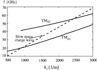
second kind, and modified Bessel functions of the first kind, respectively. Figure 2 shows the slow space-charge mode of the electron beam and the TM01and TM02waveguide modes for this Cherenkov maser experiment. From this diagram, a resonant interaction would be expected to occur around 21 GHz with the TM01mode and around 55 GHz with the TM02 mode.
The vacuum pressure and gas pressure were measured 110 cm away from the anode near the vacuum pump port and at the anode, respectively, by two active Pirani gauge heads and recorded on a two-channel digital display. The charging voltage was measured by an instantaneous capacitive voltage probe. The discharge current was monitored by an in-line current viewing resistor共CVR兲of resistance 0.066⍀.
[image:2.612.53.414.54.133.2]Fast electron beam diagnostics were designed, con-structed, and calibrated, having response times typically of a few ns, which permitted time-correlated observation of the evolution of the electron pulse parameters. The electron beam parameters measured included the beam current共using a compact Rogowski coil upstream from the interaction re-gion兲and the transported beam current共using another com-pact Rogowski coil downstream from the interaction region兲. The microwave radiation generated by the Cherenkov maser was launched by a tapered cylindrical output horn for detailed analysis. The microwave pulse duration and tempo-ral profile from the PS-based Cherenkov maser amplifier were obtained by monitoring the output of a rectifying crys-tal detector with an oscilloscope. The basic microwave mea-surement system, screened in a metal box, was composed of
FIG. 1. Cherenkov maser experimen-tal configuration.
[image:2.612.353.518.612.732.2]Ka-band共26.5–40 GHz兲or W-band共75–100 GHz兲 compo-nents starting with a small microwave receiving horn fol-lowed by a directional coupler, attenuators, waveguide, and crystal detectors. Two methods were used to identify the frequency range of the Cherenkov radiation. One technique used a series of in-waveguide cutoff filters, and the other used an interferometer. From the first method both the fre-quency and the energy distribution were obtained. The inter-ferometer was used to further confirm the frequency of the maser output.
The radiation mode pattern 共i.e., the field distribution and the power distribution兲measurements of the Cherenkov maser were conducted by scanning a radially polarized de-tector in a circular path centered on the aperture of the output horn while repeatedly pulsing the maser device. The field distribution and the power distribution are dependent on the distance from the launching antenna to the detector, which can be divided into three identifiable regions without sharp boundaries including the reactive near-field region共Rayleigh field兲, the radiating near-field region 共Fresnel region兲, and the far-field region共Fraunhofer region兲. The power distribu-tion measurements were conducted in the far-field region. For the Cherenkov maser, the diameter of the output horn was 6 cm and the dominant frequency of the source was about 25.5 GHz (⫽1.18 cm兲 and the far-field conditions required that the launching and receiving antennas should be separated by larger than 61 cm. Therefore, the detector was placed 1 m away from the launching horn. A reference de-tector system was detached and placed at a fixed position through the entire mode scanning experiment to compensate for random fluctuations in the maser output.
III. EXPERIMENTAL RESULTS
The pseudospark共PS兲discharge process was studied by monitoring the time-resolved voltage and current. The mea-sured time-correlated PS discharge voltage and current dis-played the three stages of a pseudospark discharge: 共1兲 Townsend discharge; 共2兲hollow cathode discharge; and共3兲 conductive pseudospark discharge. The Townsend discharge in the PS gives rise to a plasma, i.e., a virtual anode, extend-ing from the anode toward the cathode region. After enterextend-ing the hollow cathode region, the plasma, with almost the full anode potential, forms a high field sheath surrounding the hollow cathode surface and gives rise to a very fast increase in the emission current. A high current axial electron beam, consisting mainly of electrons from the hollow cathode re-gion behind the cathode hole, is formed during this hollow cathode discharge stage. Afterward, the discharge transfers to the final conductive phase, in which the cold cathode sur-face facing the anode takes over the whole discharge current with a very high current produced at a low acceleration po-tential until the gap is shorted.18–20
The upper part of Fig. 3 shows a typical record of the time-correlated PS discharge voltage and beam current. The beam current was recorded by a Rowgowski coil located 6 cm away from the pseudospark anode as shown in Fig. 1. A collimator of 3 mm aperture and 6 m in length separated the pseudospark anode from the beam current monitor and was
present throughout all the experiments. The duration of the hollow cathode phase of the PS discharge was adjustable between 10–50 ns. The electron beam extracted in the hol-low cathode stage had a current of 10–100 A with an accel-eration potential close to the applied voltage. The electron beam from the conductive PS discharge had a current of 100–1000 A with beam energy of a few hundred eV.
To obtain a stable, high-quality electron beam, essential for coherent microwave generation, care must be taken with appropriate gas feed and pump points and circuit parameters such as the external capacitance value, etc. Also, in order to achieve the PS hollow cathode effects our experiments showed that共1兲the cathode hole diameter should be chosen to be in the range of the cathode thickness (⬃3 mm兲; and共2兲 the hollow cathode cavity depth should have a minimum value equivalent to the thickness of the cathode.
The operation of the whole maser system is described as follows: The maser system was originally evacuated down to 2–3 mtorr at the discharge chamber and ⬃0.01 mtorr at the pumping port. The pumping port was connected at the end of the output horn using a glass T-piece chamber. Argon gas was fed into the system from the anode side at a very slow rate of 1 mtorr/s through a very fine controlled needle valve until a desired gas pressure was reached and balanced by adjustment of the needle valve. The high voltage applied across the pseudospark chamber was increased slowly until breakdown occurred. To achieve a self-pinched, high current electron beam, it was essential to match the applied charge voltage and chamber gas pressure so that the dis-charge operated in the pseudospark regime. Our experiments showed an empirical relation of VB⫽(0.20⫾0.05)
⫻p⫺4.02⫾0.18d⫺1.77⫾0.01, where VBis the breakdown voltage
[image:3.612.347.528.54.203.2]of the pseudospark discharge in kV, and p and d are the pressure in torr and the cathode–anode separation in centi-meters, respectively. The self-pinched electron beam was ex-tracted from the anode hole of the 8-gap pseudospark dis-charge chamber just before breakdown occurred and then guided along the beam tube to the Cherenkov interaction region, where the beam interacted with the modes of the dielectric lined waveguide, and the resonant wave was am-plified to a few kilowatts from a low power level of a few watts. The microwave radiation generated in the interaction
region was guided a further 60 cm in a cylindrical vacuum waveguide before being launched into free space by the coni-cal output horn. The microwave radiation was then diag-nosed by a screened and calibrated microwave diagnostic system situated in the far field of the antenna.
Microwave radiation was detected successfully from this first pseudospark-based dielectric Cherenkov maser ampli-fier. The temporal profile of the microwave output radiation from the maser is shown in the lower part of Fig. 3, time correlated with the electron-beam current and voltage pro-files. It was found experimentally that significant microwave radiation was generated only when the dielectric was present in the interaction space, although if there was no dielectric in the cylindrical waveguide, then a very small microwave emission was detected. It was also found that the microwave signal was independent of the guide magnetic field over the range 0.13 to 0.26 T, which ensured that the interaction did not depend on the cyclotron frequency of the electrons. Fur-ther frequency measurements and the scanned mode profile TM01 were consistent with the simulations, showing strong coupling with the correct mode for a Cherenkov interaction. In addition, two components of the microwave pulse were observed corresponding to the two energy components of the electron beam during the pseudospark discharge breakdown. Another interesting result was the discovery that the small microwave emission was always present even without the guide B-field or dielectric lining in the waveguide. These results demonstrated that the maser magnification grew from the emission from the PS discharge itself.14,15
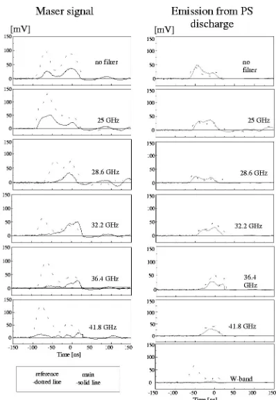
The frequency range of the microwave radiation from the Cherenkov maser amplifier was measured by applying different cylindrical cutoff filters in the waveguide and com-paring this signal with a signal from a nonfiltered reference detector. Using this method, both the Cherenkov maser out-put and the emission from the PS discharge were analyzed. Figure 4 shows the results with cutoff filters for both the emission from the PS discharge and the Cherenkov maser output signal when the applied discharge voltage was fixed at
⬃75 kV. The waveforms in Fig. 4 were acquired by a digi-tizing oscilloscope in an averaging mode of 5 shots. The results showed that the emission from the PS discharge had a wide frequency distribution but below the W-band 共62.5 GHz兲cutoff frequency. In the presence of the dielectric, the microwave output had typically two frequency components: one was between 25 and 28.6 GHz, and the other between 28.6 and 41.8 GHz. By normalizing the Cherenkov maser output signals in Fig. 4, an averaged, normalized microwave output was obtained for each cutoff filter configuration and is shown in Fig. 5. By comparing the time evolution of the beam voltage with the averaged maser output spectrum, it was found that the lower frequency microwave signal corre-sponded to a 70–80 keV beam energy from the hollow cath-ode discharge regime and the higher frequency microwave signal to the lower energy beam from the conductive phase of the pseudospark discharge. This increase in frequency with decreasing beam energy is consistent with a Cherenkov interaction mechanism.
An additional method for frequency analysis in the Cher-enkov maser was the use of an interferometer. The
interfer-ometer in a detecting box consisted of a specially made, T-shaped Ka-band rectangular waveguide junction with a
back-stop adjustor. The movement of the back-stop adjustor changed the phase of the standing wave structure in the waveguide, hence giving rise to a periodic variation of the output amplitude from the detector. The period of the output is expected to beg/2. Here,g/2 is the in-guide wavelength
of the wave to be measured. The wave frequency can then be calculated by using the following equations:
f⫽
2⫽
kc
2⫽
c
2
冑
k⬜ 2⫹k储2, 共3兲
k⬜⫽ a; k储⫽
2
g
, 共4兲
[image:4.612.338.537.50.338.2]where a is the larger dimension of the rectangular wave-guide. For a Kaband waveguide a is equal to 7.112 mm. In FIG. 4. The results with cutoff filters for both the emissions from the PS and the Cherenkov maser output signal.
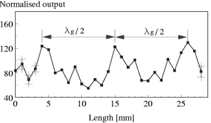
[image:4.612.330.549.614.730.2]the experiment, to reduce shot-to-shot instabilities of the measurement, a reference signal was recorded and used to normalize the main signal in each position of the back-stop adjustor; five normalized signals were averaged. A typical measurement result at an applied potential of ⬃75 kV was analyzed against the length of the back-stop adjustor and is shown in Fig. 6. From Fig. 6, g was measured to be⬃21
mm, corresponding to a frequency of 25.5 GHz. This result further confirmed that the radiation has spatial coherence.
To verify the mode of operation as TM01, the far-field output radiation pattern from the conical output horn which had an aperture diameter of 60 mm was measured. The out-put antenna pattern associated with the azimuthal E-field component was measured to be independent of the presence of the dielectric and close to zero, confirming the operation of a TM mode. Figure 7 shows the measured pattern associ-ated with the radial E-field component of the radiation with a relative error of 4% and a systematic error in the radial angle measurement of ⬍2°. The measured pattern was in good agreement with the results from bench experiments in which a 27 GHz TM01 microwave signal was launched using the same horn. Fraunhofer diffraction theory predicts a maxi-mum at 7.5°, which is in close agreement with both the Cherenkov maser experiment and bench measurements.
In order to calculate the gain of the maser amplifier, both the input power and output power of the maser amplifier were measured. The input power and output power were ob-tained by integrating the power densities over space. The integrations were completed by numerically integrating the
normalized mode profiles and multiplying with the measured maximum power density. In the experiment, there was no external input seed signal from an external microwave radia-tion source. The microwave emission from the PS discharge acted as the input signal to the amplifier, i.e., the input signal to the Cherenkov maser was generated by the pseudospark discharge itself and was consistent with experiments con-ducted by Liou et al.14 and Ramaswamy et al.,15 who ob-served a similar broadband low-power microwave signal from a pseudospark discharge. As shown in Fig. 5, the emis-sion from the PS discharge had a much wider frequency range 共22–50 GHz兲than the maser output 共mainly between 25–28.6 GHz兲. The emission from the PS discharge was also scanned and found to have similar symmetric mode profiles in both Eand Er. The total power of the emission from the
PS discharge was calculated to be 93⫾25 W in the whole frequency range of 22–50 GHz. In the frequency range of 25–28.6 GHz, the fraction of the emission power from the PS was measured to be approximately (2.7⫾0.6)% using a series of waveguide cutoff filters 共an example is shown in Fig. 4兲, resulting in an input power of 2.7⫾1.3 W to the maser at the frequency of maser amplification. With the di-electric present the maser signal was scanned and found to have a TM01 profile. The power of the maser signal was measured using a method similar to that for the background signal. Power from the Cherenkov maser amplifier of 2.0 ⫾0.2 kW was measured without considering any losses within the detecting system. The gain of the maser was there-fore calculated to be 29⫾3 dB.
The observed and measured frequency was found to be 20% higher than that predicted by the resonance condition for 70–80 keV beam energy in Fig. 2. This discrepancy is probably due to charging of the dielectric liner.13 A relative spectral energy distribution was obtained and approximately 65% of the radiation was found to lie in the 25–28.6 GHz frequency band.
IV. SIMULATIONS
A. Introduction
To complement the experimental investigations of the Cherenkov maser, a three-dimensional numerical simulation code was developed. The code integrates the Lorentz equa-tions of motion for the electrons self-consistently with Max-well’s wave equation for a single TM0n waveguide mode in the steady-state limit where the relative slippage of the ra-diation with respect to the electron beam is neglected, as in Ref. 21. It includes the effect of resonant space-charge forces and electron velocity spread.
B. Electromagnetic field evolution
We now derive equations which describe the evolution of the amplitude and phase of a TM0n mode due to its inter-action with a beam of electrons.
Maxwell’s equations in an isotropic medium can be writ-ten as
[image:5.612.69.283.54.179.2]ⵜ•D⫽, 共5兲
[image:5.612.61.292.592.731.2]FIG. 6. Frequency identification by an interferometer.
FIG. 7. Far-field mode pattern scan of the radial component Ercompared
ⵜ•B⫽0, 共6兲
ⵜ⫻E⫽⫺B
t , 共7兲
ⵜ⫻H⫽J⫹D
t . 共8兲
Taking the curl of 共8兲, using the vector identity
ⵜ⫻共ⵜ⫻A兲⫽ⵜ共ⵜ•A兲⫺ⵜ2A,
and applying共6兲and共7兲, we obtain
冉
ⵜ2⫺ 1c2
2
t2
冊
H⫽⫺ⵜ⫻J. 共9兲We assume that the electric and magnetic fields of the waveguide mode, Erad and Hrad, are of the form given by
共A2兲 and共A3兲 共see the Appendix兲, with the exception that the complex mode amplitude is now a slowly varying func-tion of space and time, i.e., G⫽G(z,t), where
冏
Gt
冏
Ⰶ兩G兩 and冏
G
z
冏
Ⰶk兩G兩,and that the transverse structure of the modes as described by
e and h is unaffected by the presence of the electron beam.
This allows共9兲to be written as
冉
2 z2⫺1
c2 2 t2⫺
2
冊
Hrad⫽⫺ⵜ⫻J.As Hrad⫽Hˆ for TM0n modes, we can write
1
2
冉
2 z2⫺1
c2
2 t2⫺
2
冊
共G共z,t兲ei(kz⫺t)兲h⫹c.c.
⫽Jz r ⫺
Jr
z , 共10兲
where we have again assumed azimuthal symmetry, i.e., /⫽0. Using the slowly varying envelope approximation
冉
2 z2⫺1
c2
2 t2⫺
2
冊
共G共z,t兲ei(kz⫺t)兲⬇2ik
冉
G z ⫹
c2k
G
t
冊
ei(kz⫺t)⫹
冉
2c2⫺k
2
冊
Gei(kz⫺t),共10兲becomes
ik
冉
Gz ⫹
c2k
G
t
冊
hei(kz⫺t)⫹c.c.⫽
冉
Jz r ⫺Jr z
冊
.共11兲 As we have assumed azimuthal symmetry, the current and charge densities driving the electromagnetic field will therefore correspond to those of thin charged rings, as shown in Fig. 8.
[image:6.612.322.525.52.195.2]The form of the current density J can be deduced from Fig. 8. Each electron represents a ring of charge q with 兩q兩
Ⰷ兩e兩, i.e.,
J⫽⫺
兺
j⫽1 N
qj
␦共r⫺rj兲
2r ␦共z⫺zj兲, 共12兲
where qj⫽2r0 j, r0 jis the initial radius of each ring and
is the linear charge density of each ring. can be deter-mined from the fact that in our steady-state model, N rings cross a fixed point z in one wave period, so that
I⫽
兺
j⫽1 Nqj
2⫽j
兺
⫽1 Nr0 j.
After evaluating the sum, this can be rearranged to give and consequently qj
qj⫽
4r0 jI
Nrb
, 共13兲
where rb is the electron beam radius. Defining J˜ as
J ˜⫽ 1
冕
0 2Je⫺i(kz⫺t)d共t兲, then
J ˜z⫽⫺
兺
j⫽1 Nqj
␦共r⫺rj兲
2r e
⫺i(kz⫺tj), 共14兲
J ˜r⫽⫺
兺
j⫽1 Nqj vr j vz j
␦共r⫺rj兲
2r e
⫺i(kz⫺tj), 共15兲 and Eq.共11兲becomes
ikdG dzhe
i(kz⫺t)⬇
冉
˜Jzr ⫺ikJ˜r
冊
, 共16兲where we have averaged over a wave period and dropped the time derivative of G, i.e., we assume steady-state amplifica-tion, so G⫽G(z). Substituting 共14兲 and 共15兲 in 共16兲, we obtain
dG dz h⫽
i
2k
兺
j⫽1 Nqj
冉
␦
⬘共
r⫺rj兲2r ⫺
␦共r⫺rj兲
2r2
⫺ikvr j vz j
␦共r⫺rj兲
2r
冊
e⫺i(kz⫺tj).
Multiplying both sides by er*and integrating over the entire
waveguide cross section gives
[image:6.612.51.301.536.669.2]冉
2冕
her*r dr冊
dG dz⫽ i
2k
兺
j⫽1 Nqje⫺i(kz⫺tj)
冕
冉
␦⬘共
r⫺rj兲⫺␦共r⫺rj兲 r
⫺ikvr j vz j␦共
r⫺rj兲
冊
er*dr. 共17兲Now
2
冕
her*r dr⫽k⑀0Q,where Q is the mode-dependent constant defined in 共A18兲. Therefore,共17兲reduces to
dG dz⫽
i
2k2⑀0Q j
兺
⫽1 Nqje⫺i(kz⫺tj)
⫻
冕
冉
␦⬘共
r⫺rj兲⫺␦共r⫺rj兲 r ⫺ikvr j vz j␦共
r⫺rj兲
冊
er*dr.共18兲 Consider the integral on the right-hand side 共RHS兲 of 共18兲. Using the fact that
er⫽
⫺ik
␣2 2
dez2 dr ⫽
⫺ik
␣22 I0
⬘共
␣2r兲,then
冕
er*共r兲␦⬘共
r⫺rj兲dr⫽⫺der* dr冏
r⫽rj
⫽⫺ikI0
⬙共
␣2r兲.Now, y⫽I0(x) satisfies the modified Bessel equation
d2y dx2⫹
1
x d y dx⫺y⫽0,
so solving for d2y /dx2 it can be shown that
冕
er*共r兲␦⬘共
r⫺rj兲dr⫽ik冉
I1共␣2rj兲 ␣2rj ⫺
I0共␣2rj兲
冊
.It is now straightforward to show that the integral on the RHS of共18兲reduces to
冕
冉
␦⬘共
r⫺rj兲⫺␦共r⫺rj兲 r ⫺ik
vr j vz j␦共
r⫺rj兲
冊
er*dr⫽⫺ik
冉
I0共␣2rj兲⫹i k␣2
vr jvz jI1共␣2rj兲
冊
,so that共18兲becomes
dG dz ⫽
1 2k⑀0Q
兺
j⫽1N
qje⫺i(kz⫺tj)
冉
I0共␣2rj兲⫹i k
␣2vr jvz jI1共␣2rj兲
冊
.Substituting for qj using 共13兲gives
dG dz ⫽
2I
k⑀0rbQ
冓
r0 j
冉
I0共␣2rj兲⫹ ik␣2
vr j vz j
I1共␣2rj兲
冊
⫻e⫺i(kz⫺tj)
冔
, 共19兲where
具
. . .典
is an average over the entire electron ensemble. This equation describes the evolution of the complex ampli-tude of a TM0n mode due to its interaction with a beam of electrons.C. Space charge
In addition to the radiation fields of the waveguide mode, the electrons will also experience forces due to space-charge fields. The analytical description of space space-charge forces in two or three dimensions is in general complicated and demanding in terms of the computer time and memory required. In this section we derive expressions for the reso-nant ac space-charge fields using a simplified model.
As in the previous sections, we assume azimuthal sym-metry. The charge density is therefore of the form
⫽⫺
兺
j⫽1 N
qj
␦共r⫺rj兲
2r ␦共z⫺zj兲
⫽⫺
兺
j⫽1 N
qj␦共r⫺rj兲
2r ␦共t⫺tj兲. 共20兲
Assuming that the charge density can be written as
⫽1 2共˜ e
i(kz⫺t)⫹c.c.兲,
multiplying both sides by e⫺i(kz⫺t) and integrating overt
from 0→2 gives
˜⫽1
冕
0 2e⫺i(kz⫺t)d共t兲
⫽
兺
j⫽1 N
qj
␦共r⫺rj兲
2r
e⫺i(kz⫺t) vz j
. 共21兲
From Gauss’s law,
ⵜ•Esc⫽ ⑀0,
so writing Escas
Esc⫽12E˜
scei(kz⫺t)⫹c.c.,
and assuming that the space-charge field acts only in the z direction, i.e., Esc⫽Esczˆ, then it can be shown, using 共21兲, that
E
˜sc⫽⫺i ˜
k⑀0⫽ i k⑀
兺
jqj␦共r⫺rj兲
2r
e⫺i(kz⫺t) vz j
. 共22兲
Note from共22兲that E˜scis infinite at r⫽rj. In order to
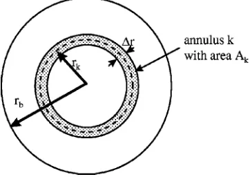
con-sider these rings as being the centers of Nr annuli, each of
equal thickness ⌬r⫽rb/Nr. The central radius of the kth
annulus is
rk⫽共k⫺ 1 2兲⌬r,
initially, so that k⫽1 is the innermost annulus, and k⫽Nr is
the outermost annulus. The initial area of the j th annulus is given by
Ak⫽
冉
rk⫹ ⌬r2
冊
2⫺
冉
rk⫺ ⌬r2
冊
2⫽2rk⌬r. 共23兲
We will average the space-charge force over the cross-sectional area of each annulus Ak so
Eksc
¯⫽ 1
Ak
2
冕
rk⫺⌬r/2 rk⫹⌬r/2
Escr dr
⫽2ik⑀0A
k
兺
j⫽1 Nkqj
e⫺i(kz⫺t) vz j
⫹c.c.,
where Nkis the number of rings lying in annulus k, i.e., with rk⫺⌬r/2⬍rj⬍rk⫹⌬r/2. Using the definition of qj in 共13兲
and the fact that in a given annulus k, ro j⫽rk for all j
⫽1, . . . ,Nk, this then becomes
Eksc
¯⫽ iINr
k⑀0rb2N
兺
j⫽1 Nke⫺i(kz⫺t) vz j
⫹c.c. 共24兲
Note that if all electrons remain within a distance ⌬r/2 of
their initial radial position, then Nk⫽N/Nr always, and共24兲 takes the particularly simple form
Eksc
¯⫽ iI
k⑀0rb2
冓
e⫺ivz
冔
k⫹c.c., 共25兲
where
具
. . .典
kis an average over the electrons within the kthannulus. Note that the space-charge field in one annulus acts only on the electrons within that same annulus and has no influence on the electrons in other annuli. Under most con-ditions, 共24兲 and 共25兲 should be almost equivalent. A case where 共25兲 would not be a good approximation would be when there is a strong dc space-charge field, and a weak guide magnetic field. In this case, the beam will spread radi-ally and the number of electrons in each annulus will change substantially from their initial values. For the parameters in
this paper, the effect of dc space-charge fields are dominated by that of the guide field and can be neglected.
D. Electron dynamics
In order to describe the interaction between the electron beam and the TM0n waveguide mode self-consistently, it is necessary to describe the motion of the electrons under the action of the fields of the waveguide mode, the space-charge fields, and the guide magnetic field B0. The force on the jth charged ring making up the electron beam is determined by the Lorentz equation
Fj⫽⫺qj共E⫹vj⫻B兲, 共26兲 where vjis the velocity of each electron comprising the ring and the electric field E is a superposition of the radiation electric fields, Erad, as given by 共A2兲 and共A9兲, and the ac space-charge field, Esc, as given by共25兲. The magnetic field
B is a superposition of the radiation fields, Brad, as given by
共A3兲and共A9兲, and the guide magnetic field B0⫽B0zˆ. This force determines the positions (rj) and scaled
mo-menta (uj⫽␥jvj) of the electrons共rings兲via drj
dt ⫽
uj
␥j 共
27兲
duj dt ⫽
Fj mj
⫽⫺ qj
mj
冉
Erad⫹Esc⫹uj
␥j
⫻共Brad⫹B0兲
冊
, 共28兲 where uj⫽␥jvj, mj⫽qjme/兩e兩 is the mass of the j th ring, me is the mass of a single electron, and ␥j⫽(1⫹兩uj兩2/c2)1/2 is the relativistic factor.
As we are describing a steady-state amplifier, it is con-venient to change the independent variable from t to z, via
d/dt→vzjd/dz so that 共27兲and共28兲become dtj
dz⫽
␥j uz
j
, 共29兲
drj dz⫽
urj uzj
, 共30兲
duj dz ⫽⫺
兩e兩 mevzj
冉
Erad⫹Esc⫹uj
␥j⫻共
Brad⫹B0兲
冊
. 共31兲 Equations 共29兲through共31兲, in combination with Eqs. 共19兲 and共25兲, form a closed system of equations which allows a self-consistent description of the Cherenkov interaction be-tween an electron beam and a TM0n waveguide mode. [image:8.612.84.265.57.185.2]E. Results
Figure 10 shows a graph of the predicted output power from the Cherenkov maser as a function of interaction length for the TM01 and TM02 modes when the beam energy is 75 keV and current is 10 A. Only these two modes lie within the frequency range of the radiation emitted by the PS discharge. The microwave power at z⫽0 was assumed to be 3 W for both modes. The electron beam was assumed to be a per-fectly collimated solid beam, with an axial velocity spread (⌬vz/vz) of 3%, and a radius of 1.5 mm. It can be seen
[image:8.612.329.558.465.566.2]from Fig. 10 that the TM01mode at⬃ 21 GHz is amplified strongly, attaining a power of ⬃3.4 kW at z⫽60 cm, whereas the power in the TM02mode at ⬃55 GHz remains around its initial level. These simulations support the inter-pretation of the experimental results as microwave amplifi-cation via a Cherenkov interaction between the high-quality electron beam and the TM01 mode of the dielectric-lined waveguide.
V. CONCLUSIONS
In conclusion, we have presented the first measurements of coherent electromagnetic radiation generation in a free-electron maser using an free-electron beam from a pseudospark discharge, which were consistent with the results from the simulations showing strong coupling with the correct mode for a Cherenkov interaction. The microwave radiation was generated by Cherenkov amplification of the broadband emission from the pseudospark discharge. A microwave emission of around 100 W from the PS discharge was mea-sured in the frequency range 20–50 GHz with a percentage of 共2.7⫾0.6兲% in the frequency range 25.5–28.6 GHz. The frequency of the microwave output after the Cherenkov ma-ser interaction was measured to be mainly around 25.5 GHz and the dominating mode was identified as being TM01. The duration of the microwave pulse was approximately 80 ns, with a peak power of around 2⫾0.2 kW. The gain of this amplifier was measured as 29⫾3 dB. The microwave output was found to be insensitive to the magnitude of the applied magnetic field, which was varied from 0.13 to 0.26 T. The observed frequency, 25.5 GHz, was found to be slightly higher than that predicted by the resonance condition for the above beam parameters and the cold alumina-lined wave-guide共21 GHz兲. This discrepancy could be explained as the effect of either the charging of the dielectric liner or the beam loading effect on the transverse structure of the TM waveguide mode.
Future fundamental aims would be to improve the per-formance of the pseudospark discharge with respect to mi-crowave power, pulse repetition frequency, and further in-vestigation of the transportation of this novel electron beam in the low pressure gas-filled interaction region. This work
could potentially lead to a whole series of novel microwave sources and amplifiers employing a pseudospark-based high-density, high-brightness electron beam.
ACKNOWLEDGMENTS
H.Y. would like to thank the Engineering and Physical Sciences Research Council 共EPSRC兲and the Committee of Vice-Chancellors and Principals of the Universities of the United Kingdom and the University of Strathclyde for finan-cial support so that this work could be started and continue. Assistance from P. Aitken and C. Whyte is also gratefully acknowledged.
APPENDIX: DIELECTRIC WAVEGUIDE MODES
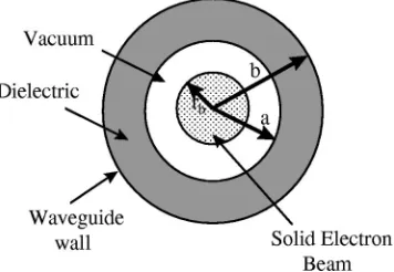
1. TM0nmodes
A diagram of the cross section of a dielectric lined cir-cular waveguide is shown in Fig. 11. In the absence of any charges or currents, Maxwell’s wave equation for the electric field is
冉
ⵜ2⫺ 1c2
2 t2
冊
Erad⫽0. 共A1兲
Let us assume that the radiation electric field in the wave-guide is of the form
Erad⫽1 2共Ge
i(kz⫺t)e共r,兲⫹c.c.兲, 共A2兲
and that the magnetic field in the waveguide is of the form
Hrad⫽12共Ge
i(kz⫺t)h共r,兲⫹c.c.兲. 共A3兲
In these expressions, G is a constant complex amplitude and
e,h are complex mode vectors.
We restrict our analysis to azimuthally symmetric TM0n modes. Substituting共A2兲into共A1兲, it can be shown that for TM0n modes, the z component of e, ez, satisfies the relation
冉
ⵜ⬜2⫹冉
⑀ 2c2⫺k
2
冊冊
ez共r兲⫽0. 共A4兲
As these modes are azimuthally symmetric, i.e., e ⫽e(r), the transverse derivative in the expression above
[image:9.612.73.275.54.186.2]re-duces to
FIG. 10. Calculated output power of TM01and TM02modes as a function
of z.
[image:9.612.349.527.58.181.2]ⵜ⬜2⫽ 2
r2⫹
1
r
r,
so 共A4兲becomes
冉
2 r2⫹1
r
r⫹
2
冊
ez共r兲⫽0, 共A5兲
where 2⫽⑀2/c2⫺k2. Equation 共A5兲 is a form of Bessel’s equation of order 0, so ezis a linear combination of
zeroth-order Bessel functions, i.e.,
ez1⫽A1J0共1r兲⫹B1Y0共1r兲 when a⬍r⬍b, 共A6兲
ez2⫽J0共2r兲⫹B2Y0共2r兲 when 0⬍r⬍a, 共A7兲 where1,22 ⫽1,2⑀1,22/c2⫺k2and A
1, B1, and B2are con-stants which are determined by the boundary conditions to be shown shortly.
2. Characteristic equation
The transverse field components can be obtained from the longitudinal field components 共A6兲 and 共A7兲 using the relations
h⬜⫽1
2共i⑀⑀0zˆ⫻ⵜ⬜ez兲,
e⬜⫽ 1
2共ikⵜ⬜ez兲,
so that the field components in each region can be written as:
共i兲 Region 1: dielectric (a⬍r⬍b)
er1⫽ ik
1共A1J0
⬘共
1r兲⫹B1Y0⬘共
1r兲兲, hr1⫽0e1⫽0, h1⫽ ⑀0⑀1
k er1
ez1⫽A1J0共1r兲⫹B1Y0共1r兲, hz1⫽0;
共A8兲
共ii兲 Region 2: vacuum (0⬍r⬍b)
er2⫽ ik
2
J0
⬘共
2r兲, hr2⫽0e2⫽0, h2⫽ ⑀0⑀2
k er2 ez2⫽J0共2r兲, hz2⫽0.
共A9兲
As r→0, Ym(2r)→⬁ for all m so B2⫽0 in order that the fields remain finite at all points across the cross section of the waveguide.
In order to determine the arbitrary constants A1, and B1, we must use the boundary conditions on E and H, at the boundaries r⫽a and r⫽b. At r⫽a, the vacuum/dielectric
boundary, the continuity of h implies that
⑀1
1共A1J0
⬘共
1a兲⫹B1Y0⬘共
1a兲兲⫽ ⑀1 2J0
⬘共
1a兲, 共A10兲and the continuity of ez implies that
A1J0共1a兲⫹B1Y0共1a兲⫽J0共2a兲. 共A11兲
At r⫽b, the dielectric/perfect conductor boundary, the
con-tinuity of ez implies that ez(r⫽rb)⫽0, so
B1⫽⫺
J0共1b兲
Y0共1b兲A1. 共A12兲
Substituting 共A12兲in共A10兲implies that
A1⫽ J0共2a兲Y0共1b兲
J0共1a兲Y0共1b兲⫺J0共1b兲Y0共1a兲 ,
whereas substituting共A12兲in共A11兲implies that
A1⫽ ⑀2 ⑀1
1 2
J0
⬘共
2a兲Y0共1b兲J0
⬘共
1a兲Y0共1b兲⫺J0共1b兲Y0⬘
共1a兲 .For these two expressions to be consistent, it is necessary that
⑀12J0共2a兲共J0
⬘共
1a兲Y0共1b兲⫺J0共1b兲Y0⬘共
1a兲兲 ⫽⑀21J0⬘共
2a兲共J0共1a兲Y0共1b兲⫺J0共1b兲Y0共1a兲兲,共A13兲 which is the characteristic equation for a TM0n mode.
In order to have a resonant interaction between the TM0n mode and an electron beam, the phase velocity in region 2
共vacuo兲must be less than c, so we consider only cases where 2
2⬍0. Defining
2⫽i␣2, and using the fact that
Jm共ix兲⫽imIm共x兲,
where Im(x) is a modified Bessel function of the first kind,
then the characteristic equation for the TM0n modes 共A13兲 becomes
⑀␣2I0共␣2a兲共J1共1a兲Y0共1b兲⫺J0共1b兲Y1共1a兲兲 ⫽1I1共␣2a兲共J0共1a兲Y0共1b兲⫺J0共1b兲Y0共1a兲兲.
共A14兲
3. Power
The flow of electromagnetic power across a surface is determined by the z component of the Poynting vector, de-fined as
S⫽E⫻H,
when integrated over the surface, i.e., waveguide cross-section area. Note that as electromagnetic energy propagates inside the dielectric, it is necessary to integrate over both regions of the dielectric, i.e., from r⫽0→b. The power at a
position z is therefore
P⫽
冕
A共E⫻H兲zdA. 共A15兲
For a TM0nmode, E⫽Errˆ⫹Ezzˆ and H⫽Hˆ , so共A15兲
becomes
P⫽2
冉
冕
0a
Er2H2r dr⫹
冕
ab
where we have used the fact that Er and H are azimuthally symmetric. Recalling that Er and H can be written in the form
Er⫽ 1 2Ge
i(kz⫺t)e
r⫹c.c., H⫽ 1 2Ge
i(kz⫺t)h
⫹c.c.,
the above can then be rewritten as
P⫽
2兩G兩 2
冉
冕
0 a
共er2h*2⫹er*2h2兲r dr
⫹
冕
a b
共er
1h*1⫹e*r1h1兲r dr
冊
.Now, from共A8兲and共A9兲
er1,2⫽ k
⑀0⑀1,2h1,2,
so
P⫽兩G兩2 k
⑀0
冉
冕
0 a兩h2兩2
⑀2 r dr⫹
冕
a b兩h1兩2
⑀1 r dr
冊
. 共A16兲Substituting for h
1,2 using 共A8兲 and 共A9兲 and setting ⑀2 ⫽1,⑀1⫽⑀ gives
P⫽12k⑀0Q兩G兩2, 共A17兲
where
Q⫽a
2
␣2
2 共I0共␣2a兲 2⫺I
1共␣2a兲2兲⫺ ⑀
1 2
J02共2a兲
共J0共1a兲Y0共1b兲⫺J0共1b兲Y0共1a兲兲2 ⫻关共J0共1a兲Y0共1b兲⫺J0共1b兲Y0共1a兲兲2⫹共J
0共1b兲Y1共1a兲⫺J1共1a兲Y0共1b兲兲2兴a2
⫹2关共J0共1b兲Y1共1a兲⫺J1共1a兲Y0共1b兲兲共J0共1a兲Y0共1b兲⫺J0共1b兲Y0共1a兲兲兴
a
1
⫺关J0共1b兲Y1共1b兲⫺J1共1b兲Y0共1b兲兴2b2] 共A18兲
is a mode-dependent constant.
1
M. A. Gundersen and G. Schaefer, Physics and Applications of
Pseudo-sparks, NATO ASI Series B, 219共Plenum, New York, 1990兲.
2K. Frank and J. Christiansen, IEEE Trans. Plasma Sci. 17, 748共1989兲. 3G. F. Kirkman and M. A. Gundersen, Appl. Phys. Lett. 49, 494共1986兲. 4
H. Riege and E. Boggasch, IEEE Trans. Plasma Sci. 17, 775共1989兲.
5
E. Boggasch and M. J. Rhee, Appl. Phys. Lett. 56, 1746共1990兲.
6W. Benker, J. Christiansen, K. Frank, H. Gundel, W. Hartmann, T. Redel,
and M. Stetter, IEEE Trans. Plasma Sci. 17, 754共1989兲.
7T. C. Marshall, Free Electron Lasers共Macmillan, New York, 1985兲. 8
S. J. Cooke, A. W. Cross, W. He, and A. D. R. Phelps, Phys. Rev. Lett. 77, 4836共1996兲.
9D. S. Lemons and L. E. Thode, Phys. Rev. Lett. 56, 2684共1986兲. 10J. E. Walsh, T. C. Marshall, and S. Schleshinger, Phys. Fluids 20, 709
共1977兲.
11
W. Peter and E. Garate, Phys. Rev. A 45, 8833共1992兲.
12W. B. Case, R. D. Kaplan, J. E. Golub, and J. E. Walsh, J. Appl. Phys. 55,
2651共1984兲.
13
E. Garate, R. Cook, P. Heim, R. Layman, and J. E. Walsh, J. Appl. Phys.
58, 627共1985兲.
14R. Liou, H. Figueroa, A. H. McCurdy, G. Kirkman-Amemiya, R. J.
Temkin, H. Fetterman, and M. A. Gundersen, Appl. Phys. Lett. 61, 2779
共1992兲.
15K. Ramaswamy, W. W. Destler, and J. Rodgers, J. Appl. Phys. 83, 3514
共1998兲.
16H. Yin, W. He, G. R. M. Robb, A. D. R. Phelps, K. Ronald, and A. W.
Cross, Phys. Rev. ST Accel. Beams 2, 020701共1999兲.
17G. Schaefer and K. H. Schoenbach, in Ref. 1, Chap. 21, p. 55. 18
P. Choi, R. Aliaga, and B. Blottiere, Appl. Phys. Lett. 63, 2750共1993兲.
19
M. P. Alberta, J. Derouard, L. C. Pitchford, N. Ouadoudi, and J. P. Boeuf, Phys. Rev. E 50, 2239共1994兲.
20A. Anders, S. Anders, and M. A. Gundersen, Phys. Rev. Lett. 71, 364
共1993兲.