ABSTRACT
CAI, AILING. Wide band gap semiconductor optical waveguide. (Under the direction of Professor John F. Muth)
This dissertation involves the design, fabrication and characterization of wide band gap semiconductor optical waveguide devices. Prism coupling was used as the primary characterization method to obtain design parameters of the refractive index and propagation loss of the wide band gap semiconductor materials such as c-plane, a-plane GaN and ZnO grown on c-plane, r-plane sapphire. AlxGa1-xN alloys and ZnO co-doped with nitrogen, tellurium and chromium diffused sapphire waveguides were also
investigated. The simulation and layout of optical waveguide devices, including 1x2 GaN splitters, Mach-Zehnder interferometers and asymmetric twin waveguide devices, were performed using a commercial software package using the beam propagation method. As-grown GaN materials were characterized by using cathodoluminescence, optical transmission measurement, atomic force microscopy and prism coupling. GaN waveguides, 1x2 splitters and Mach-Zehnder interferometers were fabricated and tested at visible wavelengths using HeNe and a tunable Argon laser. The end faces of the waveguide chips were polished by using the sample preparation techniques used in transmission electron microscopy. The morphology of the rib waveguides were
WIDE BAND GAP SEMICONDUCTOR OPTICAL
WAVEGUIDE
By
Ailing Cai
A dissertation submitted to the Graduate Faculty of North Carolina State
University in partial fulfillment of the requirements for the Degree of
Doctor of Philosophy
ELECTRICAL ENGINEERING
Raleigh, NC
2005
Approved By:
______________________________
Professor John F. MuthChair of Advisory Committee
___________________________________ _________________________________
Professor Salah M. Bedair Professor Veena Misra
DEDICATION
BIOGRAPHY
Ailing Cai, was born in Beijing, P. R. China. In 1992, she received a Bachelor’s of
Science in Applied Physics from Beijing University of Aeronautics and Astronautics. In
2000, she received a Master’s of Science in Materials Science from Southwest Missouri State
University. In August of 2000, she began her Ph.D. studies in Electrical Engineering at
North Carolina State University, and defended her dissertation on July 28 of 2005. Under the
advisement of Professor John Muth, she studied wide band gap semiconductor optical
ACKNOWLEDGMENTS
I gratefully acknowledge the contributions of many people to support the research
work described in this dissertation. First, I would like to thank my advisor, Dr. Muth, for
guiding my research. His encouragement and enthusiasm have helped me throughout my
Ph. D. study. I gained great knowledge under his advisement. I would also like to thank the
other committee members, Dr. Bedair, Dr. Narayan, Dr. Johnson and Dr. Misra for serving
on my committee and for their contributions to my research.
I would like to thank Dr. Gerhold for supporting the project and helpful discussion on
the device simulation. I also would like to thank Dr. Johnson’s group for growing GaN
samples used in fabricating waveguide devices. I would like to thank Dr. Narayan’s group
for providing ZnO co-doped with tellurium and nitrogen samples. I would also like to thank
SVT associates for providing a-plane GaN and ZnO samples. I would also like to thank Dr.
El-Masry for providing support for polishing samples. I appreciate the time Joe Matthews
has spent teaching me valuable process knowledge to fabricate the waveguide devices. I
would like to thank Dr. Voitenko for interesting discussion and help on optics. I would like
to thank my fellow graduate students—Dr. Xingquan Liu, Dr. Meredith Reed, Fude Liu,
Andrew Oberhofer, Anuj Dhawan, Yoganand Saripalli, Hugh Porter, Xiyao Zhang, Patrick
Wellenius, Daryl Fothergill, and Christian Mion, John Holland and David Nackashi for help
and support. Finally, I would like to thank my family in China for their continued support
and encouragement throughout my Ph. D. study. I would like to thank my husband, Hugh,
TABLE OF CONTENTS
Pages
LIST OF TABLES... viii
LIST OF FIGURES ... ix
Chapter 1 INTRODUCTION...1
1.0 Introduction...1
1.1 Outline of the dissertation...7
1.2 References...10
Chapter 2 REVIEW OF OPTICAL WAVEGUIDE BASICS...14
2.1 Three-layer asymmetric dielectric slab waveguides ...14
2.1.1 Transverse electric(TE) mode...16
2.1.2 Transverse magnetic field(TM) mode...19
2.2 Rectangular dielectric waveguides ...20
2.3 Graded-index waveguides...24
2.4 Numerical method for solving arbitrary shaped waveguides ...26
2.4.1 Finite difference method...27
2.4.2 Finite element method...27
2.5 Numerical method for the propagating wave...28
2.6 References...30
Chapter 3 WIDE BAND GAP OPTICAL PLANAR WAVEGUIDE ...32
3.1 Using prism coupling to characterize the optical properties of materials...32
3.3 Refractive indices of a-plane GaN grown on r-plane sapphire ...40
3.4 Changes in ordinary and extraordinary refractive indices of doped ZnO...49
3.4.1 Experimental procedures ...50
3.4.2 Results and discussions...52
3.5 Refractive indices of ZnO thin films grown on r-plane sapphire ...57
3.5.1 Experimental details...58
3.5.2 Results and discussions...59
3.6 Fabrication and characterization of chromium-diffused waveguides...63
3.6.1 Experimental details...65
3.6.2 Results and discussions...66
3.7 Characterization of ZnO grown on Cr-diffused sapphire waveguide...72
3.8 Propagation loss of GaN materials at wavelength of 632.8 nm...75
3.9 Summary...80
3.10 References...82
Chapter 4 SIMULATION OF OPTICAL WAVEGUIDE DEVICES...85
4.1 Y-junction splitter ...85
4.2 Mach-Zehnder interferometer...87
4.3 An example simulation of a 1.5 µm Mach-Zehnder interferometer ...92
4.4 Asymmetric twin-waveguide of GaN wide band-gap materials...99
4.5 Mask layout...111
4.5.1 Mask layout of the 1x2 GaN splitters ...112
4.5.2 Mask layout of Mach-Zehnder interferometers ...113
Chapter 5 CHARACTERIZATION AND LIGHT COUPLING INTO
WAVEGUIDE DEVICES...120
5.1 Materials growth and fabrication ...120
5.2 Materials and devices characterization ...122
5.3 Coupling system design ...129
5.4 Calculation of theoretical coupling coefficient...147
5.5 Laser light coupled into waveguide devices ...152
5.5.1 Light coupled into the GaN rib waveguides ...152
5.5.2 Light coupled into 1x2 GaN splitters...154
5.5.3 Light coupled into Mach-Zehnder interferometers...160
5.6 References ...164
Chapter 6 CONCLUSION AND FUTURE DIRECTIONS...165
6.1 Summary of work performed...165
LIST OF TABLES
Pages
Table 3-1 Fitting results of Cauchy dispersion relationship for GaN and AlxGa1-xN
materials...39
Table 3-2 Lattice constants of c-, a-plane GaN, ZnO, and c-, r-plane sapphire...41
Table 3-3 Growth conditions for as-grown ZnO (A3), ZnO doped with nitrogen (A1,
A2 and C2), ZnO doped with tellurium (B1), ZnO doped with nitrogen and
tellurium (C1)...51
Table 3-4 Fitting results of Cauchy dispersion relationship for as-grown ZnO (A3),
ZnO doped with nitrogen (A1, A2), ZnO doped with tellurium (B1), ZnO
doped with nitrogen and tellurium (C1) films, post-annealed ZnO( A3ann) in
a furnace and ZnO doped with nitrogen (A2ann, C2) annealed in the furnace,
in situ at 750 oC for 1 hour respectively ...56
Table 3-5 Fitting results of Cauchy dispersion relationship of TEmin and TEmax for a-
plane ZnO film...61
Table 5-1 Parameters used for polishing the two end-face of the sample ...122
Table 5-2 Refractive indices and film thickness measured by prism coupling system ...124
Table 5-3 Beam spot sizes at different locations for single mode lensed fiber and
coreless lensed fiber...142
Table 5-4 Design parameters of the coupling system with the BK7 ball lens based on
the simulation results and the matrix calculation...146
Table 5-5 Design parameters of the coupling system with the sapphire ball lens based
LIST OF FIGURES
Pages
Figure 1-1 A schematic diagram of the optoelectric integrated circuit ...8
Figure 2-1 The three-layer dielectric waveguide structure ...15
Figure 2-2 TE mode in the asymmetric waveguide ...17
Figure 2-3 The graphical plot of the Equation 2.19 for a three layer asymmetric
Waveguide ...19
Figure 2-4 The cross section view of a dielectric rectangular waveguide is represented
in Marcatili’s method...21
Figure 2-5 Mode conversion in a 3-D optical waveguide...22
Figure 2-6 A guide mode in a graded index is to be oscillatory in high-index regions and
exponentially damped in low-index regions...24
Figure 3-1 Prism coupling system setup...34
Figure 3-2 Index ellipsoid of GaN without an applied electric field ...37
Figure 3-3 Optical absorption spectra of GaN and AlxGa1-xN materials, where x=0, 0.18,
0.27, 0.34, 0.38 and 1...38
Figure 3-4 (a) Ordinary refractive indices (b)extraordinary refractive indices of GaN
and AlxGa1-xN materials change with wavelengths in the visible region ...40
Figure 3-5 (a) GaN crystal structure, (b) a-plane GaN grown on r-plane sapphire ...41
Figure 3-6 (a) SEM image of the a-plane GaN and (b) the c-plane GaN (note the
Figure 3-7 Reflectivity of TE polarized light changes a function of incident angles for (a)
GaN film with thickness of 1.315 µm, on a miscut r-plane sapphire. (b) for a -plane GaN sample with thickness of 8 µm. In the thicker film there was also an anomalous double dip in the reflection spectrum ...44
Figure 3-8 Refractive indices for TE mode change with angle for sample with thickness
of 8µm represented by the green curve, for sample with thickness of 1.31 µm represented by the red curve. Theoretical fit for equation (3.3) with
experimental data of maximum and minimum refractive indices of TE
mode for the thick (8 µm) and thin (1.31 µm) samples, represented by the pink and blue curves, respectively. The black curve is the theoretical fit by
using ordinary and extraordinary refractive indices of c-plane GaN...45
Figure 3-9 The dispersion of the refractive indices for TE and TM modes change with
wavelength for (a) a-plane GaN with thickness of 8 µm and c-plane GaN (b) a-plane GaN with thickness of 1.318 µm and c-plane GaN ...47 Figure 3-10 (a) CL image of the a-plane GaN with thickness of 8 µm, (b) a SEM image
of the GaN sample with thickness of 1.315 µm...48 Figure 3-11 (a) A typical XRD pattern of ZnO thin film, (b) low resolution TEM image
of as-grown ZnO doped with nitrogen sample (A2) and (c) low resolution
TEM image of as-grown ZnO sample ...52
Figure 3-12 AFM images of as-grown ZnO and ZnO doped with nitrogen film, where
a) is ZnO (A3) film, b) is the ZnO doped with nitrogen (A2) film in the size
ZnO doped with tellurium (B1) and ZnO doped with nitrogen and tellurium
(C1) films at RT. (b) Refractive index measurements at 632.8 nm of as-grown
ZnO (A3) and post annealed ZnO (A3ann), ZnO doped with nitrogen
(A2ann, C2)...54
Figure 3-14 The ordinary (a) and extraordinary (b) refractive indices of as-grown
ZnO (A3), ZnO doped with nitrogen (A1), ZnO doped with tellurium (B1),
ZnO doped with nitrogen and tellurium (C1) films fit to the Cauchy
dispersion relationship ...56
Figure 3-15 (a) XRD θ-2θ scan for a 1.0-µm-thick ZnO film grown on r-plane sapphire. (b) X-rayφ-scans for ZnO ((1010)and sapphire (0006) reflections ...59 Figure 3-16 (a) The refractive indices of the a-plane ZnO film for the TE mode
waveguide propagating in the plane at an azimuthal angle θ with respect to
the c-axis of the ZnO film (b) refractive indices of TEmin, TEmax and TM of
a-plane ZnO thin film and no, ne of c-plane ZnO thin film fit to the Cauchy
dispersion relationship ...61
Figure 3-17 Important energy levels of Cr3+ in ruby. The separation between 2A and
levels are 29 cm-1, not to scale...64
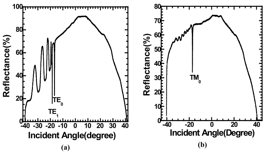
Figure 3-18 (a) TE polarized light coupled into Cr doped sapphire waveguide, (b) TM
polarized light coupled into Cr doped sapphire waveguide...67
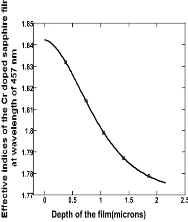
Figure 3-19 The effective indices change as a function of doping profile ...68
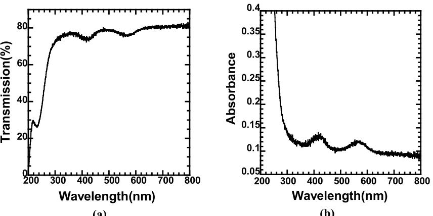
Figure 3-21 (a) Transmission spectrum of Cr doped sapphire waveguide (b) Absorbance
spectrum of Cr doped sapphire waveguide...70
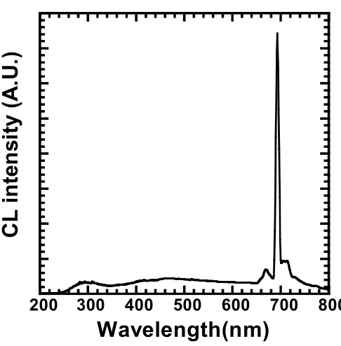
Figure 3-22 Cathodoluminescence of Cr diffused sapphire waveguide ...71
Figure 3-23 Light is coupled into the Cr-diffused waveguide...71
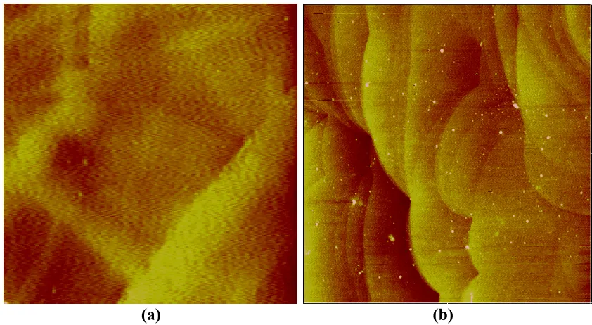
Figure 3-24 AFM images of ZnO thin film grown on (a) sapphire (0001), (b) Cr-
diffused sapphire in the scan size of 5 µm by 5 µm...73
Figure 3-25 (a) optical transmission spectra of ZnO grown on Cr-diffused sapphire, ZnO
grown on c-plane sapphire and Cr-diffused sapphire. (b) Absorbance spectra
of ZnO grown on Cr-diffused sapphire, ZnO grown on c-plane sapphire and
Cr-diffused sapphire...74
Figure 3-26 Reflectivity changes as a function of incident angles for ZnO grown on
Cr-diffused sapphire, ZnO grown on c-plane sapphire and Cr-diffused sapphire
samples...75
Figure 3-27 Reflectivity of TE polarized light changes as a function of incident angle
for (a) Al0.3Ga0.7N sample (b) Mg:GaN sample...76
Figure 3-28 Light intensity changes as a function of distance for Al0.3Ga0.7N sample ...77
Figure 3-29 Light intensity changes as a function of distance for Mg:GaN sample ...78
Figure 3-30 AFM images of (a) Al0.3Ga0.7N and (b) Mg:GaN samples in scan size of
10 µm by 10 µm...79 Figure 4-1 A transverse modulator has voltage applied perpendicular to the direction of
light propagation ...90
Figure 4-3 The cross section view of the single mode GaN Mach-Zehnder interferometer
structure at the input...93
Figure 4-4 The mode profile of the Mach-Zehnder interferometer at the input ...93
Figure 4-5 (a) The mode profile of the input of the Mach-Zehnder interferometer without
SiO2 buffer layer (b) The mode profile of the input of the Mach-Zehnder
interferometer with 0.4 µm buffer layer of SiO2...94 Figure 4-6 The half-splitting angle of the Y-branch is defined. (Note the difference in
X and Z scales.)... 95
Figure 4-7 Output power of one arm of the Y-branch splitter change as a function of the
half splitting angle...96
Figure 4-8 The Mach-Zehnder interferometer with constructive interference at the output
obtained without applied voltages ...97
Figure 4-9 Refractive index change profile obtained with applied voltages of 18V ...98
Figure 4-10 Output power of the Mach-Zehnder interferometer change with applied
Voltages ...99
Figure 4-11 The top view of the asymmetric twin-waveguide structure ...100
Figure 4-12 The image shows the cross section view of the laser portion of the
asymmetric twin waveguide structure. The color bar is the normalized
refractive inde ...102
Figure 4-13 The amplitude profile of the first super mode in the ATW structure
changes with different layers ...103
Figure 4-14 (a)The amplitude profile of the second super mode in the ATW structure
super mode in the ATW structure change with the thickness of layers...104
Figure 4-15 The cross section view of the first supermode profile obtained from the
BPM ...105
Figure 4-16 Effective refractive indices change as a function of the width of the active
waveguide ...106
Figure 4-17 Effective refractive indices change as a function of the width of the passive
waveguide ...107
Figure 4-18 Powers transfer from the active waveguide to the passive waveguide along
the propagation direction ...107
Figure 4-19 Cross section view of the contour map of the mode 00 at Z=0 µm ...109
Figure 4-20 Cross section view of the contour map of the power transferred from the
active waveguide to the passive waveguide at Z=350 µm...110
Figure 4-21 Cross section view of the contour map of the power confined in the passive
waveguide at Z=460 µm ...111
Figure 4-22 Mask layout of the 1x2 GaN splitters ...113
Figure 4-23 Cross section view of the processing flow of the Mach-Zehnder
interferometers (a) ridge etching by BCl3, (b) depositing SiO2 as the buffer
layer for metal electrode, (c) Ohmic contact etching, (d) Schottky contact
deposition, (e) Ohmic contact deposition ...114
Figure 4-24 Mask layout of ridge etching of Mach-Zehnder interferometers by using
R-Soft software ...115
Figure 4-25 Mask layout of SiO2 buffer layer for Mach-Zehnder interferometers ...116
Figure 5-1 (a) Cathodoluminescence spectrum of GaN materials, (b) Optical
transmission spectra of GaN materials with Al0.25Ga0.75N and Al0.3Ga 0.7N
materials as lower cladding...123
Figure 5-2 Reflectivity changes as incident angle changes ...124
Figure5-3 (a) 5µm by 5 µm scan of as–grown GaN (b) 5µm by 5 µm scan of GaN after dry etching ...125
Figure 5-4 An AFM image of the ridge profile of GaN waveguide in the scan size of 20 µm by 20 µm ...126
Figure 5-5 The cross section view SEM image of the input of the GaN waveguide...127
Figure 5-6 A SEM image of the GaN splitter...128
Figure 5-7 A SEM image of the transition region of the GaN splitter ...128
Figure 5-8 A coupling system consisting of a lensed fiber and a ball lens, where p0 is the input plane located at the beam waist of the lensed fiber, p1 is the output plane...131
Figure 5-9 This set up is used to align the lensed fiber and the ball lens ...133
Figure 5-10 The lensed fiber is aligned with the ball lens...133
Figure 5-11 (a) An image of a lensed-fiber taken by using a SUMITOMO splicer, (b) a microscopy image of the lensed-fiber in the refractive index matching fluid...135
Figure 5-13 The far field pattern of laser light at a wavelength of 632.8 nm propagates
through the lensed fiber formed by the single mode fiber (a) at 5 inches
away from the tip of the lensed fiber, (b) at 10 inches away from the tip of
the lensed fiber...137
Figure 5-14 The far field pattern of the laser light at a wavelength of 632.8 nm
propagates through the lensed fiber formed by the coreless fiber (a) at 5
inches away from the tip of the lensed fiber (b) the coreless fiber at 10
inches away from the tip of the lensed fiber ...138
Figure 5-15 (a) The far field pattern of the laser light at a wavelength of 632.8 nm
propagates through the lensed fiber formed by a coreless lensed fiber
connected to a straight coreless fiber with length of 1 mm fused to a single
mode fiber. (b) Schematic view of the coreless lensed fiber was fused to
the coreless fiber connected to the single mode fiber ...138
Figure 5-16 Mode profiles of laser light at wavelength of 632.8 nm was traveling
through the single mode lensed fiber in (a) the single mode fiber part,
(b) in the deformed lensed fiber region, (c) at the end of the lensed fiber,
(d) at 114.4 µm away from the tip of the lensed fiber ...140
Figure 5-17 Mode profiles of laser light at the wavelength of 632.8 nm was traveling
through the coreless lensed fiber in (a) the single mode fiber part, (b) the
coreless fiber region, (c) at the tip of the lensed fiber, (d) at further way
distances from the tip of the lensed fiber ...141
Figure 5-18 Propagation of Gaussian beam through a ball lens. The dimensions of the
Figure 5-19 The fundamental mode profile of the ridge waveguide at wavelength of
1.55 µm are (a) in x direction, (b) in y direction...148
Figure 5-20 (a) The Gaussian beam waist radius changes as a function of Z-Zw, (b)
The Gaussian beam curvature changes as a function of Z-Zw ...150
Figure 5-21 Coupling efficiencies change as a function of (a) axial and (b) transverse
displacement ...151
Figure 5-22 The coupling setup for GaN waveguide devices...153
Figure 5-23 Light at a wavelength of 632.8 nm is coupled into the GaN waveguide ...153
Figure 5-24 Light at a wavelength of 632.8 nm is coupled into the 1x2 GaN waveguide
splitter ...154
Figure 5-25 Coupling setup is used for imaging the end face of the 1x2 GaN splitter
Chip...155
Figure 5-26 By shining the light directly to the end face of the GaN splitter chip, images
were taken, (a) outputs of a 1x2 GaN splitter with distances of 125 µm
between the two bright spots, (b) outputs of two different splitters, the
distance between them are 250 µm...156
Figure 5-27 (a ) An image of the output of a splitter when light is coupled into the
splitter, (b) far field pattern of the light propagates through the splitter...157
Figure 5-28 The Laser light with a wavelength of 514.5 nm is coupled into a 1x2 GaN
splitter ...158
Figure 5-29 Shows the far field pattern of modes of the 1x2 GaN splitter at a wavelength
of 514.5 nm ...158
Splitter...159
Figure 5-31 Light with a wavelength of 476.5 nm propagates in the 1x2 GaN splitter ..160
Figure 5-32 Laser light at a wavelength of 632.8 nm is coupled into the Mach-Zehnder
interferometer...160
Figure 5-33 Light at a wavelength of 514.5 nm is coupled into the Mach-Zehnder
interferometer...161
Figure 5-34. The output image of the GaN Mach-Zehnder interferometer (a) by shining
light directly to the end face of the chip, (b) by coupling the laser light at
wavelength of 514.5 nm into the Mach-Zehnder interferometer...162
Figure 5-35. The far field pattern of the laser light propagating through the GaN
Mach-Zehnder interferometer at a wavelength of 514.5 nm changes with
temperature decreasing (a) at the beginning of 1s, at the end of 1s, (c) at
the beginning of 2s and (d) at the end of 2s...163
CHAPTER 1
INTRODUCTION
1.0 Introduction
In this dissertation, Gallium Nitride (GaN) waveguide devices such as straight waveguide, 1x2 splitters, Mach-Zehnder interferometers and Asymmetric Twin-Waveguide (ATW) are designed based on the simulation results by using beam propagation method (BPM) software. GaN straight waveguide, 1x2 splitters and Mach-Zehnder interferometers are fabricated. Visible light is coupled into GaN waveguide devices. This is a first attempt to study GaN optoelectronic devices integration on the sapphire substrate. The light coupling issues for small dimension of GaN waveguide devices with large numerical apertures are addressed. The emphasis of the study is experimental research and development of GaN optoelectronic integration. The objective of this dissertation is to provide insight on GaN waveguide devices design and challenging issues related to GaN-based optoelectronic waveguide devices.
spectrum. In addition, they are potential materials for high temperature and high power electronic devices due to their wide band gap energy, wurtzite structure, good thermal conductivity and high break down voltage. GaN-based heterojunction bipolar transistor (HBT) and heterojunction field-effect transistor (HFET) technologies are also being investigated intensively for microwave applications4, in particular, high electron-mobility transistor (HEMT) devices have been most successful5.
The properties of group-III nitride semiconductors were first investigated in the 1970s by Pankove and others6,7. Researchers were successful at synthesizing GaN crystals with efficient blue and UV photoluminescence and cathodoluminescence. However, they were unable to grow smooth epitaxial films suitable for heterostructure or to achieve the acceptor doping of p-type GaN based materials.
Significant progresses in GaN semiconductor studies were made in the 1980s. Amano and co-authors proved that the growth of smooth GaN films was possible by using a very thin buffer layer of AlN at the GaN and sapphire interface8. The buffer layers serve to relax the lattice mismatch strain and to promote 2D growth. Therefore, they improve the quality of GaN films on lattice–mismatched substrates such as sapphire.
Nakamura fabricated a GaN p-n junction light emitting diode1. On November 1993, Nichia announced the first commercial blue GaN LED’s1.
In 1996, InGaN multi-quantum-well(MQW) structure laser diodes were fabricated from III-V nitride materialsfor the first time by Nakamura and colleagues11. In 1998, the high-power InGaN-based blue laser diodes with a long lifetime were demonstrated by Nakamura. The threshold current densities of these laser diodes were 1.2 kA/cm2. The threshold voltages as low as 4.3 V have been achieved. The output power is as high as 420 mW per facet under room-temperature continuous wave operation12.
More recently, for use in electronic device application, a high performance double-heterostructure AlGaN/GaN field effect transistor with gate length of 0.4 µm grown on SiC (0001) substrate has been achieved. The maximum transconductance of the HFET transistor is 180 mS/mm. The high electron mobility of the 2D electron gas, excellent current
saturation characteristics and pinch-off characteristic have obtained up to a high temperature of 400 oC13,14. By employing InGaN as a channel layer instead of GaN, the
AlGaN/InGaN/GaN double heterostructure with higher carrier density and stronger carrier confinement has been investigated15. The enhanced HFET device performances are expected. Also, high performance of AlGaN/GaN HEMT with gate length of 0.2 µm can reach maximum drain current density and extrinsic transconductance as high as 1.4 A/mm and 266 mS/mm, respectively16.
the low resistance metal contacts to GaN semiconductors, especially p-type, and materials with high Al percentages of AlGaN semiconductor are needed to improve the efficiency of the GaN-based electrical and optical devices. The third issue, which is of important to the research of this project, is the challenge of coupling. In visible spectrum region, in order to design single mode GaN waveguide devices, the rib width of GaN waveguide structures is in the submicron range. The mode field diameter is small. This reduction in size is due to order of magnitude scaling with the wavelength relative to comparable infrared optoelectronics. Also, large refractive index difference between the GaN and sapphire substrate results in large numerical aperture of GaN waveguide devices. Even worse, the mode field diameter of fiber is larger than the mode field diameter of the GaN waveguide, since the refractive index difference of the core and cladding layer is small. Numerical aperture of the fiber is small compared to GaN waveguide. In order to efficiently couple the laser light into the GaN waveguide devices, the phase and amplitude distribution of the fiber and GaN waveguide mode need be matched.
A fourth issue of consideration, no attempts have been made to produce integrated optical circuits on GaN. The development of GaN-based light emitting diodes,
ZnO is II-VI semiconductor compound, which is similar to GaN, with band gap energy of 3.37eV at room temperature and wurtzite crystal structure. ZnO is another promising material for application in electronic and optoelectronic device structures in the ultraviolet (UV) to vacuum-UV(VUV) spectral region18. ZnO has exciton binding energy of 60 meV19, which is large. For ZnO, the electro-optic coefficients of γ33 (for TE wave) and γ13 (for TM wave) at wavelength of 632.8 nm are 2.6 pV/cm and -1.4 pV/cm when c-axis is in the a-plane, respectively. A-plane ZnO thin film is also an important material for acousto-optic20, piezoelectric21 and optical modulator22 device applications when it is grown on
r-plane(1102)sapphire substrate.
Historically, the primary devices in optoelectronic integrated circuits are based upon III-V semiconductor materials. Optoelectronic integrated circuits (OEIC’s) consist of photonic components and electronic components on the same chip. Because of their
potential of achieving compactness, high performance as well as low costs, they are attractive for optical communication systems. Monolithic integration of optical amplifiers with
waveguides and lasers has been fabricated in GaAs and InP-based materials23. For example, integration of laser and waveguide using a twin-guide(TG) structure has been realized on InP-based materials24. A fully integrated 1.55 µm wavelength continuously tunable
Several other non-semiconductor materials have been widely applied in integrated optical circuit and optoelectronic circuits. Lithium niobate oxide (LiNbO3) is an important material for integrated optical devices due to large electro-optic coefficients and forming low
loss waveguide. The largest electro-optic coefficient for LiNbO3 is
r
33 with value of 30.9pm/V at wavelength of 0.633 µm30. When an electrical filed is applied along the z-axis of LiNbO3, a change in refractive index in z direction is proportional to the applied field, the
proportional constant is
r
33. This is referred to the linear electrooptic effect. By using theelectrooptic effect, LiNbO3 can be used in modulation and switching functions. The directional coupler, Mach-Zehnder interferometer, the polarization modulator have been widely studied. A major drawback of LiNbO3 is that lack of direct materials integration ability onto the same substrate with semiconductor lasers and high-speed electronic devices.
Compound semiconductor alloys such as gallium-aluminum arsenide (AlxGa1-xAs) and indium-gallium arsenide-phosphide (In1-xGaxAsyP1-y) are well applied in integrated
optical devices and optoelectronic integrated circuits. For GaAs,
r
41 is 1.1 pm/V atwavelength of 0.9 µm. Although their electro-optic coefficients are lower than LiNbO3, they can be integrated with lasers, detectors, switches, electro-optic modulators, field effect transistors and high speed electronics on the same substrate. Also, by engineering of the GaAs based and InP based materials forming quantum wells structures, based on the free carrier induced refractive index change and electro-absorption induced refractive index change effects, switches and modulators with high performance can be realized.
GaN-based optoelectronic devices, such as, InGaN-AlGaN LEDs, GaN
sapphire substrate. Also, GaN based-waveguide devices are transparent in the visible and near infrared optical spectra. GaN materials grown on sapphire as dielectric waveguide with large refractive index differences provide advantages to make small sized, compact optical devices and interconnections. The modal confinement is strong due to the high refractive index difference between the core and cladding layers waveguide.
A monolithic, dual-wavelength blue/green light emitting diode consisting of two InGaN/GaN multi-quantum-well segments separated by a p++/n++ GaN tunnel junction has been demonstrated31. The linear electro-optical coefficient of wurtzite GaN was reported. At
632.8 nm, the electro-optical coefficients of
r
33 andr
31 are 1.91 and 0.7 pm/V, respectively32.By utilizing the effect of thin-film induced refractive index change, GaN channel waveguide have been investigated33. Their potential applications as the waveguide coupler for optical communication in infrared region have been investigated34. Propagation loss of GaN-based ridge waveguide at wavelength of 488 nm was measured35. These advancements in GaN based materials motivate the new development of monolithic integrated optical circuits using Ga(In,Al)N materials.
1.1 Outline of the dissertation
optoelectronic devices. The scattering losses of GaN materials are also critical for
waveguide devices. The less scattering losses of the GaN materials, the better performance of the waveguide devices is to transmit light. Using the knowledge of the refractive index and scattering losses data, it is possible to fabricate and characterize the GaN waveguide devices. This can demonstrate that the advantages of GaN on sapphire waveguide devices employed in compact interconnection due to the large refractive index difference between the core and cladding layer, which lead to better model confinement and less radiation bending loss.
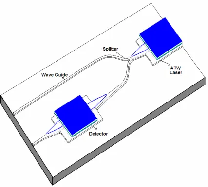
The subject of this dissertation is to advance the state of the art of visible optical integrated circuits conceptually first. This is shown in Fig. 1-1.
The design and theory of the asymmetric twin-waveguide (ATW) structure will be presented, as well as a fabrication of Mach-Zehnder interferometer. ATW structure design integrates the application of GaN for optical pumping into sapphire. ATW structure is an important element as a mode converter in optoelectronic integration. In order to obtain high performance of GaN ATW structure, a GaN laser needs to be made first. From GaN
optoelectronic circuit design point view, ATW structure of GaN materials is one of the key devices need be addressed.
In the present study, refractive index of GaN related materials as an important parameter for optoelectronic devices design are investigated systemically. ZnO materials have similar band gap energy and crystal structure to GaN. The refractive index of ZnO and related materials are investigated due to the close band gap energy and in plane lattice constants. Finally, GaN waveguides, 1x2 splitters and Mach-Zehnder interferometers devices are fabricated and characterized. The new coupling system consisting of the lensed fiber and a ball lens system is designed. The laser light at visible range is coupled into GaN waveguides, 1x2 splitters and Mach-Zehnder interferometers by using a HeNe laser and a tunable Argon laser.
In this dissertation, chapter 2 discusses some of the basic theory on electromagnetic wave propagation in dielectric waveguide and numerical simulations. Many of the principles introduced in chapter 2 will be applied in later chapter.
diffused sapphire waveguide, which will be employed into the integration with ATW structure in the later chapter. Propagation loss of GaN materials is studied.
Chapter 4 presents the simulation results of the ATW structures, 1x2 GaN waveguide splitters and Mach-Zehnder interferometers waveguide devices. Mask layout of 1x2 GaN waveguide splitters and Mach-Zehnder interferometers are presented.
Chapter 5 is dedicated to the GaN waveguide devices fabrication and characterization. It also includes the coupling system design, coupling efficiency study and light coupling into the GaN waveguide devices.
Chapter 6 concludes with a discussion of the GaN waveguide devices study and future work.
1.2 References
1 Shuji Nakamura, Gerhard Fasol, The Blue Laser Diode: GaN Based Light Emitters and Lasers (Berlin: Springer-Verlag, 1997).
2 A. G. Bhuiyan, K. Sugita, K. Kasashima, A. Hashimoto, A. Yamamoto, and V. Y. Davydov, Applied Physics Letters 83, 4788-4790 (2003).
3 Y. Li, Y. Liu, H. Shen, M. Wraback, M. G. Brown, M. Schurman, L. Koszi, and R. A. Stall, Appl. Phys. Lett. 70, 2458 (1997).
4 A. Wieszt, R. Dietrich, J. -S. Lee, et al., in Proceedings of European Symposium on Gallium Arsenide and Related III-V Compounds Applications (Paris, 2000), P. 260. 5 OKI Electric Power Transistor for Wireless Communications Achieves World's-Best
6 J. I. Pankove, J. E. Berkeyheiser, and E. A. Miller, Journal of Applied Physics 45, 1280-1286 (1974).
7 J. I. Pankove and J. E. Berkeyheiser, Journal of Applied Physics 45, 3892-3895 (1974).
8 H. Amano, N. Sawaki, I. Akasaki, and Y. Toyoda, Applied Physics Letters 48, 353-355 (1986).
9 H. Amano, M. Kito, K. Hiramatsu, and I. Akasaki, Jpn. J. Appl. Phys. 28, L2112 (1989).
10 T. Tanaka, A. Watanabe, H. Amano, Y. Kobayashi, I. Akasaki, S. Yamazaki, and M. Koike, Applied Physics Letters 65, 593-594 (1994).
11 S. Nakamura, T. Mukai, M. Senoh and N. Iwasa, Jpn, J. Appl. Phys., 31, L139-L142 (1992).
12 S. Nakamura, Journal of Crystal Growth 195, 242-247 (1998).
13 N. Maeda, T. Saitoh, K. Tsubaki, T. Nishida, and N. Kobayashi, Jpn, J. Appl. Phys., 38, L987 (1999).
14 N. Maeda, K. Tsubaki, T. Nishida, and N. Kobayashi, Jpn, J. Appl. Phys., 38, L799 (1999).
15 C. X. Wang, K. Tsubaki, N. Kobayashi, T. Makimoto, and N. Maeda, Applied Physics Letters 84, 2313-2315 (2004).
16 A. Jimenez, Z. Bougrioua, J. M. Tirado, A. F. Brana, E. Calleja, and E. Munoz and I. Moerman, Applied Physics Letters 82, 4827 (2003).
18 D. C. Look, D. C. Reynokls, C. W. Litton, R. L. Jones, D.B. Eason, and G. Gantwell, Appl. Phys. Lett. 81, 1830 (2002).
19 D. M. Bagnall, Y. F. Chen, Z. Zhu, and T. Yao, Appl. Phys. Lett. 73, 1038 (1998). 20 M.-S. Wu, A. Azuma, T. Shiosaki, and A. Kawabata, Journal of Applied Physics, 62,
2482-2484 (1987).
21 N. W. Emanetoglu, S. Liang, C. R. Gorla, Y. Lu, S. Jen, and R. Subramanian, Ultrasonics Symposium, 195-200 (1997).
22 J. M. Hammer, D. J. Channin, and M. T. Duffy, Appl. Phys. Lett. 23, 176 (1973). 23 K. R. Oh, J.-H. Ahn, J. S. Kim, S. W. Lee, H. M. Kim, K. E. Pyun, and H. M. Park,
Electronics Letters 32, 39-40 (1996).
24 P. V. Studenkov, M. R. Gokhale, J. C. Dries, and S. R. Forrest, Photonics Technology Letters, IEEE 10, 1088-1090 (1998).
25 H. Wang, C. Li, and S. R. Forrest, Photonics Technology Letters, IEEE 15, 1189-1191 (2003).
26 H. Matsueda, S. Sasaki, and M. Nakamura, Lightwave Technology, Journal of 1, 261-269 (1983).
27 M. Makiuchi, O. Wada, S. Miura, H. Hamaguchi, H. Machida, K. Nakai, H. Horimatsu, and T. Sakurai, Int. Electron Devices Meet. Tech. Dig. (San Francisco, CA), 862 (1984).
28 M. Kuno, T. Sanada, H. Nobuhara, M. Makiuchi, T. Fujii, O. Wada, and T. Sakurai, Applied Physics Letters 49, 1575-1577 (1986).
30 A. Yariv, Optical Electronics in Modern Communications.
31 I. Ozden, E. Makarona, A. V. Nurmikko, T. Takeuchi, and M. Krames, Applied Physics Letters 79, 2532-2534 (2001).
32 X.-C. Long, R. A. Myers, S. R. J. Brueck, R. Ramer, K. Zheng, and S. D. Hersee, Applied Physics Letters 67, 1349-1351 (1995).
33 E. Kim, B. Lee, A. Nahhas, and H. Kim, Appl. Phys. Lett. 77, 1747 (2000).
34 R. Hui, S. Taherion,Y. Wan, J. Li, S. X. Jin, J. Y. Lin and H. X. Jiang, Appl. Phys. Lett. 82, 1326 (2003).
CHAPTER 2
REVIEW OF OPTICAL WAVEGUIDE BASICS
An optical waveguide consists of the higher refractive index core layer, with
dimension being comparable to the wavelength of the light propagating in the guide, and
surrounding cladding layers with lower refractive index. When certain discrete
electromagnetic resonances are confined in the higher refractive index layer of the waveguide,
they correspond to modes of the waveguide. Each mode has its own propagation constant,
which is the kz vector in the propagation direction. A single mode waveguide can only
support one bound mode known as the fundamental mode. The geometric parameter values,
refractive indices and the source wavelength are the key values for determination of the
single mode waveguide. The waveguide propagation constants and field profiles are
essential for the design and successful operation of optical devices.
Optical waveguide analysis is important to evaluate the field profile of the waveguide
and has been extensively developed1. It requires the understanding of the electrodynamics of
the propagation waves. The electric field E(x,y,z) and magnetic field H(x,y,z)of the
2.1 Three-layer asymmetric dielectric slab waveguides
In the three-layer dielectric optical waveguide shown in Fig. 2-1, z direction is the
direction of light propagation. We assume that the waveguide structure with thickness of d
and refractive index of n1 is homogeneous in the z direction. Also, the refractive index of the
substrate (n2) is larger than the refractive index of air (n0 = 1), but smaller than the refractive
index of the thin film (n1). For dielectric materials, which is nonconductive, J=ρ=0, we
get
ε
1=
ε
r1ε
0andn1 = εr1 . Similarly, we obtainn2 = εr2 . Together they satisfy:0 2
1 n n
n > > (2.1)
Figure 2-1. The three-layer dielectric waveguide structure.
Since the critical angle of θcs at the thin film and the substrate interfaceis given by
) ( sin
1 2 1
n n
cs
− =
θ (2.2)
And the critical angle of θc0 at the thin film and air interface is
1 0 1 0 sin n
n
c
− =
θ (2.3)
cs
θ θ > >
90 (2.4)
Total reflection occurs at both interfaces, resulting in the light trapped in the thin film with
thickness of d. On the other hand, when θ is smaller than θcsand θc0 <θ< θcs, part of the light radiate into the substrate and form the substrate radiation modes.
One more condition required for the internally reflected light traveling in the core
region without loss is the self-consistency condition2. It means that the ray after reflections at
the interfaces of the air-film and film-substrate is phase shifted by 2(n+1)π, where n is an
integer. Then the constructive wave is formed. Since the internally reflected light undergoes
a phase shift of π radians at the air film interface, the same beam reflects again at the film
substrate with another phase shift of π radians, resulting in a total phase shift of 2π radians.
Then the total reflective phase shift for the light propagating through the waveguide material
is related to the wave’s path:
d m
2 ) 90
sin( −θ = λ (2.5)
where m=n+1, m is the mode number, which is an integer with a value greater than 0; d is the
distance between the reflecting surfaces; θ is shown in Fig. 2-1.
In order to find the propagation constant of kz of the guided mode, the eigen-equation
of the guided mode can be calculated by using Maxwell’s equations and boundary conditions.
2.1.1 Transverse electric (TE) mode
Figure 2-2. TE mode in the asymmetric waveguide.
The electric field components are given by
Ey=0 (2.6)
Ez=0 (2.7)
) exp( ) exp(
0 y ik z
C
Ex = −α − z y>0
C1cos(kyy+φ)exp(−ikzz) 0>y>-d (2.8)
) exp( )] (
exp[ 2
2 y d ik z
C α + − z y<-d
Based on boundary conditions where Ex and Hz are continuous at the interfaces of
y=0, y=-d, by solving the wave equation of Ex, theeigenvalue equation for the TEm mode is given by π α α m k k d k y y
y = + +
− −1 2 tan 1
tan (2.9)
Where 2 1 2 2 0 2 2 ) ( c n kz ω
α = − , (2.10)
2 1 2 2 2 2 2
2 ( )
c n kz ω
2 1 2 2
2 1 2
)
( z
y k
c n
k = ω − (2.12)
Also, for a confined mode, kz is in the range of
c n k c
n
z 1
2 ω
ω
<
< .
If α2 in Equation 2.11 is less than the zero, Ex will become oscillation in the substrate.
It can result in the substrate leaky modes. If α is less than zero, the wave becomes a
propagating wave traveling through the slab layers.
With known ky, kz, α and α2, using the normalization condition in which the total
guided power is assumed to be 1 W/cm2, we can get the C
0, C1 and C2 in Equation 2.8.
Furthermore, we can get the electric field profile of a mode.
For a three-layer asymmetric waveguide, for example, the refractive index of TE
modes of the GaN film is given by 2.3529, the refractive index of TE modes of the substrate
is 1.7654. The wavelength of the light is 0.6328 µm. The thickness of the film is 2.0085 µm.
Graphical construction for solving the characteristic of Equation 2.9 is shown in Fig. 2-3. By
using MATLAB program, the left- and right- hand sides of Equation 2.9 are plotted as a
function of kz. The intersection points are the solutions of the Equation 2.9. From the
intercepts of the curves, the effective indices of the eigenmodes can be obtained. Also, Fig.
Figure 2-3. Shows the graphical plot of Equation 2.9 for a three layer asymmetric waveguide
with film thickness of 2.0085 µm.
2.1.2 Transverse magnetic field (TM) mode
For the transverse magnetic field (TM) mode, they are given by
Hy=0 (2.13)
Hz=0 (2.14)
) exp( ) exp(
0 y ik z
C
Hx = −α − z y>0
C1cos(kyy+φ)exp(−ikzz) 0>y>-d (2.15)
Similarly, we can get the guidance conditions for TMm modes.
π ε
α ε ε
α ε
m k k
d k
y y
y = − + − +
2 2 1 1 0
1
1 tan
tan (2.16)
For isotropic materials, refractive index of n1 is same for TE mode and TM mode.
For uniaixal materials, refractive index of n1 for TE mode is different from TM mode. They
can be expressed as ordinary refractive index of no1 andextraordinary refractive index of ne1
for TE mode and TM mode, respectively. Similarly, n2 can be represented as no2, ne2 for TE
and TM mode. Therefore, for uniaxial crystal, n1 and n2 should correspond to ordinary
refractive index of the thin film (no1) and the substrate (no2) in equation 2.9, extraordinary
refractive index of the thin film (ne1) and the substrate (ne2) in equation 2.16.
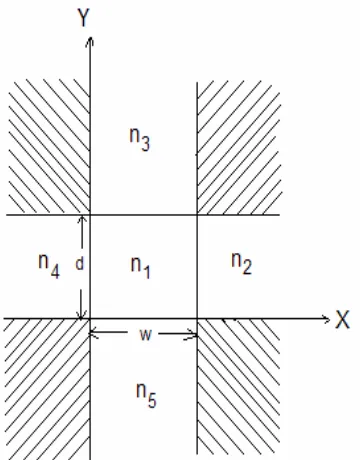
2.2 Rectangular dielectric waveguides
The rectangular dielectric waveguide is a widely used structure in integrated optics,
especially in the semiconductor diode laser, the directional coupler. The analytical method
used to solve the rectangular waveguide here is Marcatili’s method3. The core region has
higher refractive index of n1 than the cladding regions with refractive indices of n2, n3, n4, n5
shown in Fig. 2-4. The electromagnetic field in the shaded areas in Fig 2-4 can be neglected
in Marcatili method. This is because the electromagnetic field of the well-guides mode
Figure 2-4. The cross section view of a dielectric rectangular waveguide is represented in
Marcatili’s method.
The guided modes in 3-D optical waveguide are hybrid modes1. A hybrid mode is a
combination of a TE mode, in whichEy ≡0, and TM mode, in whichHy ≡0. They are
different from the normal TE mode (Ey=0, Ez=0) and a TM mode (Hy=0, Hz=0) in 2-D slab
waveguide mentioned above. In order to avoid confusion, we define the modes as Ex
whenEy ≡0and Ey whenHy ≡0. Since the width (w) of the 3-D optical waveguide is not
infinite shown in Fig. 2-5, the reflection angles of the rays which propagate in the z direction
are not zero. The Ex and Ey modes in 3-D optical waveguide have all electromagnetic components except Ey and Hy. The Ex and Ey modes represented as the solid line and the
dashed line in Fig. 2-5, respectively. Hence, in 3-D optical waveguide, the modes are
classified as
1. Expq modes: Hy and Ex are the main components; Ey, Ez, and Hz are small,
Where the subscripts p and q represent the mode order in the x and y directions.
Figure 2-5. Mode conversion in a 3-D optical waveguide.
If we only consider the main components of Ex
pq and Eypq, by ignoring the shared area
shown in Fig. 2-4, for Expq mode, since the wave propagate in the - z direction, the wave
equation of Hy is given by
0 )
( 2 222
2 2 2 2 = + − ∂ ∂ + ∂ ∂ y z H c n k y x ω (2.17)
Where c is the velocity of light traveling in vacuum and given by
0 0 1 µ ε = c .
Using boundary conditions, we can get the eigenequations of modes of Expq for a 3-D
rectangular optical waveguide as following:
) ( tan ) (
tan 1 3 1 5
y y y k k q d
k = π + − γ + − γ (2.18)
) ( tan ) ( tan 4 1 4 1 2 1 2 1 x x x k k p w k ε ε γ ε ε γ π + − + − = (2.19) Where 2 2 1 2 2 2 2 c n k k
2 2 2 2 2 2 2 2 c n k
ky z ω
γ + + =
− (2.21)
2 2 3 2 2 2 2 3 c n k
kx z ω
γ + + =
− (2.22)
2 2 4 2 2 2 2 4 c n k
ky z ω
γ + + =
− (2.23)
2 2 5 2 2 2 2 5 c n k
kx z ω
γ + + =
− (2.24)
And the optical phases ψ, θ are given by
,...) 2 , 1 ( , =
= pπ p
ψ (2.25) ,...) 2 , 1 ( , =
=qπ q
θ (2.26)
For Eypq modes, the wave equation is given by
0 )
( 2 222
2 2 2 2 = + − ∂ ∂ + ∂ ∂ x z H c n k y x ω (2.27)
The eigenequations of modes of Eypq are given by equations of
) ( tan ) ( tan 5 5 1 1 3 3 1 1 y y y k k q d k ε γ ε ε γ ε π + − + −
= (2.28)
) ( tan ) (
tan 1 2 1 4
x x x k k p w
k = π + − γ + − γ (2.29)
Also, kz, the propagation constant, can be determined by
) ( 2 2 2 2 1 2 2 y x
z k k
c n
2.3 Graded-index waveguides
Waveguides formed by diffusion with non-abrupt changes in composition instead of
epitaxial growth with abrupt composition shifts have graded refractive indices. In a graded
index waveguide, the refractive index change with position transverse to the direction of
propagation direction. The index gradient can be modeled as a series of thin homogeneous
layers, each with a refractive index n(y), where y is the distance from the surface to the thin
layer. When n(y) vary slowly with position of y, the core region of the waveguide will
confine an oscillatory wave function with an amplitude changes and phase changes with
position shown in Fig. 2-6. While in the cladding there is an exponentially decaying
function. Also, the interface that separates the core from the cladding is not well defined.
We can consider the wave travel in the graded-index medium to be similar to the wave travel
in a potential of V(y), which is a function of position. In quantum mechanics, this type of
problem can be solved by using WKB (Wentzel, Kramers, Brillouin) approximation4.
Figure 2-6. A guide mode in a graded index is to be oscillatory in high-index regions and
exponentially damped in low-index regions.
0 ) ) (
( 2 2 2 2
2 2 = + − ∂ ∂ x z E c y n k y ω (2.31)
Since n(y) changes with position of y, then ky(y) changes with y. The total electric
field solution can be given as
z j y s jk
e
e
E
z
y
E
=
− ( ) − β0
0
)
,
(
(2.32)Inserting equation (2.32) into (2.31), and define a series expansion for s(y) as
...
)
(
1
)
(
1
)
(
)
(
2 20 1
0
0
+
+
+
=
s
y
k
y
s
k
y
s
y
s
(2.33)We get the following:
2 2 2 0 1 2 0 0 2 0 2 2 0 1 2 0 0
0 ' ( )]
1 ) ( ' 1 ) ( ' [ )) ( '' 1 ) ( '' 1 ) ( ''
( s y
k y s k y s k y s k y s k y s
jk + + − + +
−
0 )] (
[ 2 2
0
2 + =
−
+ β k n y (2.34)
Since k02 can’t be zero, for the first order of approximation, s0' term, we get
0 ) ( ) ( ' 2 2 0 2
0 + −n y =
k y
s β (2.35)
From above equation, we obtain
φ
β +
−
=
∫
dyk y n y
s y 2
1 2 0 2 0 2
0( ) [ ( ) ] (2.36)
Where φ is an integration constant. The integral limits are defined based on the
boundary conditions.
For the mth-order mode, the integral upper limit is defined as the turning point at
s a m y m dy k y n k t φ φ π β = + + −
∫
2 1 2 0 2 ) ( 02( ) ]
[ (2.37) And 2 0 2 )) ( ( k m y
n t = β (2.38)
The phase change at the air and film surface is given by
] ) ) ( ( [ tan 2 2 2 1 0 2 0 2 2 0 1 k n n k a a β β γ φ − −
= − (2.39)
Where n0 is the maximum refractive index. And
na
is the refractive index of the air.Alsoγ =1for TE mode. ( 0)2
a
n n =
γ for TM mode. The phase change 2φsat the turning point
is given byπ/2 for both TE and TM mode5.
If the effective indices for different order modes are known, the WKB method can be
used to model the effective index changes as a function of depth based on equation of 2.39.
This has great potential as a tool to model the experimental information determined using
prism coupling methods. Therefore, in combination with understanding the associated
physical process, the refractive index profile due to diffusion can be determined.
2.4 Numerical method for solving arbitrarily shaped waveguides
Understanding the analytical solutions of waveguide is very helpful in the design of
geometrics. For the tapered waveguide or arbitrary shape waveguides, numerical methods
are more useful for finding guided mode solutions. The finite difference method6 and the finite element method7 are two most commonly used numerical methods.
2.4.1 Finite difference method
The finite difference method is based on the Taylor expansion to solve the partial
differential equations with boundary conditions of the system. The derivatives at a point are
replaced by difference quotient over a small interval. For example, x ∂
∂φ
is replaced by x ∆
∆φ
when ∆xis small. The finite difference solution involves the 3 steps. First, the region of interest is divided positionally into a grid of nodes. Second, the given differential equation is
replaced by an approximately difference quotient equation which approximates the analytic
equation at a point and relates to neighboring points. Third, the difference equations are
solved at each point by imposing values to the boundary conditions. The eigenvalues of the
difference equations are the propagation constants of individual modes. The eigenvectors are
the field profiles. The selection of the original grid size is checked to ensure the difference
small enough so that the solution converges.
2.4.2 Finite element method
In the finite element method, the region is discretised into a number of sub-regions
with certain shape, such as a triangle shape. This procedure is called meshing. The functions
vertices of the element. The function is commonly referred to as the shape function. Then all
elements in the solution region are assembled. Also, appropriate boundary conditions must be
imposed on the edge of the computational windows since the elements are finite space. For
instance, an electric field between parallel plates of a capacitor, one of the boundary
conditions is Ey(0)=Ey(d)=0, which is imposed to the boundary. Then, by assembly of the
elemental equations, the final system equations can be attained. The eigenvalues of the
equations are the propagation constants of the individual mode. And the eigenvectors are the
field profiles. Finite element method extends the concept of the finite difference method
subdivision of the domain to arbitrary shapes. The advantage of finite element method is the
ability to treat geometrically complex structure.
2.5 Numerical method for the propagating wave
It is also important to determine the propagation characteristics of the field, as well as
knowing the modal properties of electromagnetic fields. The beam propagation method
(BPM) is a powerful technique with which one can obtain the numerical solutions of the
propagation properties of the wave8. BPM is essentially useful for solving light propagation
in dielectric optical waveguides of arbitrary shape. In this method, a spatial mode is
decomposed into a superposition of plane waves. Each wave propagates a small distance
through the dielectric structure of interest. The plane waves are then added back together to
reconstruct the mode.
u
k
k
y
u
x
u
k
i
z
u
(
(
))
2
2 2 2 2 2 2−
+
∂
∂
+
∂
∂
=
∂
∂
(2.40)Where kis a constant number to be chosen to represent the average phase variation of
the fieldφ(x,y,z)=u(x,y,z)eikz. If the input field is known, u(x,y,z), the above equation
determines the evolution of the field in the space z>0.
In this dissertation the waveguide analysis relies on numerical calculations with the
commercial beam propagation software. The program is based on a finite difference beam
propagation method to solve the paraxial approximation of Helmholtz equation. The
“transparent” boundary conditions 9 are applied.
When applying the beam propagation method, it is assumed that the refractive index
differences along the propagation direction of the dielectric waveguide are small. This
implies that the reflected waves can be neglected. From the design point of view, in order to
avoid the reflected wave, for a taper waveguide, the width change of the taper along the z
direction should be slow so that there is no radiation loss. It is also called an adiabatic taper.
When the input field and the refractive index distribution of the waveguide structures are
known, the total path of the beam traveling can be divided into small step size of ∆Z. If large
steps of ∆Z are chosen, the numerical calculation may not converge. The simulation would
then fail. Thus, the suitable step length should be chosen through simulation to obtain the
desired degree of accuracy.
Also, when the paraxial light propagates along the Z direction and the polarization
effects can be neglected, the BPM simulation is run with the assumption of scalar field where
the average phase variation of the field in z-direction is a constant. When polarization effects
If we consider the polarization coupling and hybrid modes due to geometric effects such as
the rectangular structure of the waveguide with sloping walls, the full vectorial BPM is
chosen to run10.
The beam propagation method requires a finite solution space and hence it is
necessary to apply boundary condition so that the reflected radiation at the boundary is
“absorbed”. As mentioned above, the transparent boundary condition9 (TBC) is imposed
when the BMP simulation is performed. In this boundary condition, radiation is allowed to
freely escape without appreciable reflection. Thus, radiation flux back into the region is
prevented. The field is assumed to behave as exponentially decaying near the boundary in
TBC.
2.6 References
1 M. Koshiba, Optical Waveguide Analysis (1992).
2 B. E. A. Saleh, M. C. Teich, Fundamentals of photonics (1991).
3 E. A. J. Marcatil, Bell System Technical Journal 48, 2071-2102 (1969).
4 D. J. Griffiths, Introduction to quantum mechanics (1994).
5 R. H. Dicke and J. P. Wittke, Introduction to quantum mechanics (1960).
6 G. D. Smith, Numerical solution of partial differential equations: finite difference
methods (1985).
7 C. Johnson, Numerical solution of partial differential equations by the finite element
method (1987).
9 G. R. Hadley, Quantum Electronics, IEEE Journal of 28, 363-370 (1992).
CHAPTER 3
WIDE BAND GAP OPTICAL PLANAR WAVEGUIDE
3.1 Using prism coupling to characterize the optical properties of
materials
When a non absorbing dielectric layer with thickness comparable to the wavelength
of interest is deposited on a planar substrate, and the thin film has a higher refractive index
than the substrate, the structure forms a dielectric waveguide. The thin film can be deposited
by variety of techniques including metalorganic chemical vapor deposition (MOCVD),
molecular beam epitaxy (MBE), sputtering, and pulsed laser deposition (PLD). In this thesis
MOCVD and PLD were used to grow thin films such as Gallium Nitride (GaN), its alloys
(AlxGa1-xN) and Zinc Oxide (ZnO) on sapphire substrates.
A dielectric waveguide structure is used in a wide variety of optical devices including
semiconductor lasers, optical modulators, Mach-Zehnder interferometers, splitters and
interconnects. GaN materials grown on sapphire form a novel dielectric waveguide, the
refractive index contrast between the GaN and sapphire is much larger than the refractive
index difference usually used in glass waveguide devices, which provide advantages to make
refractive index difference between the core and cladding layers. By engineering band gap
energy of GaN and AlN alloys to form AlxGa1-xN with different Al concentration, waveguide
structure can be constructed such that GaN is the core layer with higher refractive index,
AlxGa1-xN with lower refractive index as the cladding layers. This waveguide is also
transparent for light of wavelengths longer than the absorption-edge of GaN layer since the
optical absorption edge is at 3.4 eV (365 nm). This makes the materials suitable for visible
and NIR waveguide application.
The dielectric waveguide with a layer of thin film grown on a semiconductor
substrate also can be employed as a useful structure to determine the refractive index and
thickness of the thin film by prism coupling technique. The refractive index and film
thickness are the critical parameters for designing optical devices. They can be measured by
using prism coupling system. As shown in Fig. 3-1, the prism coupling system is composed
of a prism placed closely on top of a dielectric thin film mounted on the rotational stage, an
air gap formed between them controlled by a pneumatically operated coupling head. The
rutile (TiO2) prism was used to couple light into the air/thin film/sapphire waveguide
structure. An air gap less than half of the wavelength of the source light is created between
the prism and the sample. At a certain discrete mode angle, when an incident light from the
prism is coupled into the thin film layer by the evanescent wave, the sharp drop of
reflectivity is detected by the detector and recorded by a computer. The reflectivity changing
as a function of rotation angle can be plotted. When a thin film is thick enough to confine
two or more modes, the film thickness and the refractive index with high accuracy can be
Figure 3-1. Prism coupling system setup
In centrosymmetric materials the refractive index of the film is isotropic and the
situation is easier to understand. In non-centrosymmetric materials such as those studied in
this thesis, the refractive index varies in relation to the optical axis of the crystal. For uniaxial
c-plane GaN and ZnO thin film grown on c-plane sapphire substrate, with transverse electric
(TE) field mode measurement, indices for both guides and substrate materials can be
measured in the in-plane direction. With transverse magnetic (TM) field mode measurement,
refractive indices along the c-axis direction can be measured. Since the c-axis of the crystal
(the optical axis) is perpendicular to the surface, the modes will not be dependent on the
azimuthal position of the sample.
When GaN or ZnO thin films are grown on r-plane sapphire, a-plane GaN or ZnO
thin films can be obtained and the optical situation is more complicated. When the incident
polarized light is rotated or the thin film waveguide is rotated about the axis perpendicular to