A High Performance Scan Flip-Flop Design
for Serial and Mixed Mode Scan Test
S.Vijay Murugan
1, R.Deepthi Muthulakshmi
2, S.Jayashree
3, S.Swathi
4, N.Udhayavalli
5Associate Professor, Department of ECE, Adhiyamaan College of Engineering, Hosur, Tamilnadu, India1
U.G. Student, Department of ECE, Adhiyamaan College of Engineering, Hosur, Tamilnadu, India2
ABSTRACT:The leisure of examine and high test insurance has made serial scan architecture growth widespread industrial acceptance. There are penalties correlated with the serial scan architecture which comprises of performance overhead, test data volume, test application time, and test power dissipation. The performance overhead of scan architecture is due to the scan multiplexers supplementary to the inputs of every flip-flop. For very immense-acceleration architectures with minimum conceivable combinational depth, the performance overhead provoked by the scan multiplexer has become magnified. Hence, to maintain circuit performance, the timing overhead of scan architecture must be consigned. Our perception is to design a contemporary scan flip-flop that eradicate the performance overhead of serial scan and discards the scan multiplexer from the functional path which leads to reform the functional frequency of performance critical architectures. Furthermore, the proposed architecture can be pre-owned as a common scan flip-flop in the “mixed scan” test wherein it can be pre-owned as a serial scan cell as well as a Random Access Scan (RAS) cell. The mixed scan test architecture has been implemented using the proposed scan flip-flop. The experimental results show a promising reduction in interconnects wire length, test time, and test data volume, compared to the state-of-the-art RAS and multiple serial scan implementations.
KEYWORDS:Scan flip-flop, serial scan test, random access scan test, mixed mode scan test, low power test, test application time, test data volume.
I.INTRODUCTION
Scan architecture is the only discrete Fourier transform access that can effectively analyse an eminently convoluted architecture with very immense fault coverage. The objective of scan architecture is to accomplish full controllability and observability of every flop in the architecture. In full scan architecture, each flip-flop is replaced by a scan flip-flip-flop.
A scan flip-flop is nothing but a muxed input master-slave based d type flip-flop.the scan multiplexer has two inputs: Data Input (D) and ScanInput (SI). The input excerpt is performed using a control signal called a Test Enable (TE). In functional mode, data input is excerpted and the scan flop functions as a legitimate flip-flop. In test mode, scan input is excerpted, and all the scan flip-flops connect in a serial fashion to form one or more serial shift register(s). The serial shift register(s) is popularly known as scan chain(s). All flip-flops of the scan chain are burdened with desired data by consecutive application of the clock signal. A full scan design diminishes the sequential test obstacle to combinational test obstacle.
combinational path betwixt two flip-flops. However, in a scan inserted sequential circuit the same critical path is elongated by a scan multiplexer situated at the confine of the combinational path. The scan design also augments an extra fan-out at the output of a flip-flop.
Figure 1.1 (A)Critical Path of Sequential Circuit
Figure 1.1 (B)Critical Path After Scan Insertion
Figure 1.1. Scan design performance overhead
A couple of these factors accrual the critical path delay henceforth dwindles functional clock acceleration by 5% to 10%. This composes it crucially directing towards eradicating the performance overhead of the scan multiplexer. Disparate elucidations have been proposed to alleviate the performance penalty of scan design. One analogous elucidation that alleviates the performance overhead, in conjunction with the alternative penalties correlated with the serial scan design is the applicability of partial scan contrary to full scan. In partial scan design, only a fragment of all flip-flops in Circuit-Under-Test (CUT) is recouped by scan flip-flops to articulate the scan chain. This fragment does not append flip-flops of the critical paths, henceforth dwindles the performance penalty of the scan. Furthermore, this partial scan design techniques also dwindle test data volume and test application time that precisely analogous to test-cost. Nonetheless, the partial scan design techniques may front rank to lessen flawanalysis of the cut. The excerpt of flip-flops to be appended into partial scan design can be testability measures based [3]-[6], structure-based [7]-[10], orAutomatic Test Pattern Generation (ATPG) based [11]-[13].
The structure-based techniques elective flip-flops to cut-off the feedback path. These techniques manipulate the heuristics based on network topology for electing the merest set of flip-flops and do not peculiarly evaluate the circuit behaviour. The ATPG based tacticselect flip-flops that are favourable for test generation. These techniques cardinally avail sequential ATPG to engender test vectors for all possible flaws. Further flaws which persist ephemeral, the pertinent flip-flops are endowed and these are comprised in partial scan design. Most ovate partial scan accessions crave computationally exacting sequential ATPG, and cannot be sustained with consistently proliferating circuit ramification. Besides, partial scan design tactics do not provide high fault coverage as equipped by the full scan design, and it is strenuous to consolidate them into the extant industrialized design flow. Another advent for eradicating performance penalty of scan design is to avail scan cell designs that afford tremendous performance.
II.RELATEDWORK
recouped with Muxed Input D flip-flop (MD flip-flop) besides ordinarily acknowledged as scan cell. The inputs and outputs of these scan chains are contrived into primary inputs and primary outputs. Thus in the course of test mode, all flip-flops can be precisely controlled and observed by serially shifting in/out the logic states into the shift register. At the same time, the full scan design eradicates the sequentiality of the test generation problem; the multiplexer of the scan flip-flop enumerates delay commensurate to two gate-delays in all clocked paths and thus vitiates the functional speed. In order to accomplish the insistence for high-performance systems, avail of appropriate combative performance progress tactics, in the manner that least possible logic depth designs, inflate the obligation to eradicate the scan multiplexer performance penalty [2].
The originator J.TTudu has designed a joint-scan DFT architecture to minimize test time, pattern volume, and power. He proved that serial scan DFT methodology has been very advantageous for the last couple of decades, primarily because of its simplicity. The architecture is cost-efficient in terms of hardware area and the number of test pins. Nonetheless, in later years it has been recognized that the serial scan architecture is no protracted “the solution” for a test. Designs are progressively more complicated and impenetrable with every new generation of technology. As a result of a breakneck hike in the convolution of designs newer threats for testing are revealed. Test power, test data volume, and test time are becoming intrusively high. These parameters additionally follow the trend of Moore’s law. The inflation in test time and test data volume directly impact the test cost. The exorbitant test power, particularly the dynamic power, causes test inadequacy and chip bruise which discursively enumerates to test expenditure [18]. Considerableelucidations to assuage the disproportionate power dissipation have been proposed in recent past. In contempt of all these concoctions the higher power dissipation while test still endures as one of the provocations in serial scan architecture.
The scripter F.Yang, S. Chakravarty, N. Devta-Prassana describes improving the detect ability of resistive open faults in scan cells in which it has been delineated that almost half of the transistors in extensive industrial designs may dwell in the scan chains. Habitually flaws in the cells of scan chains are approved using sequences of 0s and 1s called flush tests. Besides, automatic test pattern generation (ATPG) tools provoke tests for stuck-at faults (SAFS) and transition delay faults (TDFs) on the inputs and outputs of the scan cells. Aforementioned tests are called ATPG boundary SAF/TDF tests. These tests simultaneously with the flush tests are invoked as the extant tests for scan cells in this paper. It has been erect that the extant tests disregard innumerable flaws intramural to the scan cells. These flaws may induce blunders during the functional mode of operation if left obscured [19].
In contemporary precedent, Baik and Saluja have contemplated a few creative alternatives to the elemental RAS architecture to overthrown routing congestion issue. Baik and Salujacontemplated an enhanced versioncalled progressive random access scan (PRAS) design to enhance test time and routing wire length. The PRAS design avails separate row and column address decoders in place of a single address decoder. Baik and Saluja have shown that the arrangement of RAS cells in a square grid of size √n×√n is most advantageous for enhancing routing congestion, where n is the number of scan cells [15]. Mudlapur et al additionally addresses the routing congestion problem by eradicating the scan-in and test-enable lines. Nonetheless, it acquaints an additional gate delay in the clock path due to clock gating.
Galbi and Basto [14] contemplated a dual-edge pulse triggered scannable flip-flop which is a tremendous performance and crouched power scan cell. In a contemporary endeavour [2], Alahawat et al. Avail a modified scan cell wherein the scan multiplexer is illuminated the functional path by employing the sovereignmaster latch for functional and test mode. These high-performance scan cell designs can eradicate the performance overhead of scan designs. Nonetheless, akin scan cells cannot be availed in mixed scan test architecture. V. Kevraj, S. Vijay Murugan has done "Test design Generation sharing sweep sequence in square dimension" in which they depict a test compaction method under straightforward output for gatherings of rationale obstructs whose essential data sources and yields are scanned [22].
M. B. Aswini, R. Chitra, S. Gopika Devi, S. Vijay Murugan has done "Simulated high speed fault injection in arithmetic unit using Verilog HDL", in which they have portrayed about the FPGA - based blame infusion device called FIMTO for assessing the computerized frameworks demonstrated by Verilog HDL. This proposed work will likewise be a measurement for measuring the power of a framework in many ways and this technique has full controllability and perceptibility [23].
R. K. Rajeshwari, B. Thabasum, M. Yuvarani, E. Krishnaveni and S. Vijay Murugan has done " A combination of low power TPG & LFSR with FPGA implementation" in which a successful low power test pattern generator (LPTPG) had been proposed to diminish the test control and uses an adjusted compelled pseudo - irregular example generator to deliver seeds and then work with the single info changing generator and an exclusive OR exhibit. Consequently obliged pseudo - arbitrary flag input changing groupings are created, which incredibly limit the exchanging exercises and test control. LTPTG additionally diminishes the instantaneous from infringement contrasted with traditional LFSR [24].
III. EXISTING SYSTEM
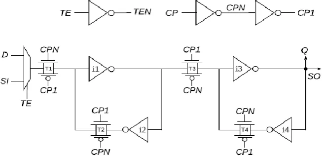
A conventional scan flip-flop design is shown in Figure 3.2. This scan cell is a master-slave latch based positive edge triggered muxed input D type flip-flop [19]-[20]. The transmission gate T1 and the inverter pair connected back to back via transmission gate T2 forms the master latch. The slave latch comprises of transmission gate T3 and the inverter pair connected back to back over transmission gate T4. The multiplexer at the input of master latch selects between functional input (D) and scan input (SI) depending upon the value of test control signal test enable (TE). In test mode, when TE is high (1), SI is selected and is connected to master latch’s input. When the clock signal (CP) is low (0), the value of SI propagates to the master latch. In the meanwhile, the slave latch retains the value from previous clock cycle. The value latched into the master propagates to slave latch when CP turns to high (1), and to the output Q of scan flip-flop. Correspondingly, when the test enable signal (TE) is set to 0, functional input D is selected, and the circuit operates in functional mode.
IV. PROPOSED SYSTEM
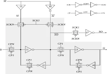
The proposed scan flip-flop schematic design is shown in Figure 4.3. Instead of a multiplexer at master latch’s input, the proposed design helps an independent path for loading test vector values into the master latch. Furthermore, the proposed scan flip-flop uses a low cost dynamic slave latch for relocating of test vectors in test mode. In functional mode, functional slave latch’s output Q drives the combinational circuit inputs. The master latch of proposed scan flip-flop is formed by transmission gate T1, and inverter pair (i1, i2) connected back to back via transmission gate T2. Similarly, the slave latch is formed by transmission gate T3, and inverter pair (i3, i4) connected back to back via transmission gate T4. The dynamic slave latch comprises transmission gate T7 and inverter i7. The test mode path is formed by adding transmission gate T5, T6, buffer i5, and inverter i6 to the master latch architecture. It should be noted that the extraneous gates added to master stage to form the test mode input path are not on the functional path.This extraneous circuitry debris paralysed during functional mode and the proposed scan flip-flop acts as a traditional flip-flop. The master latch and the slave latch are restrained by functional clock signal CP. The test mode input path is paralysed by test enable cum scan clock signal SCK.
4.1 FUNCTIONAL MODE:
The proposed scan flip-flop works as a traditional flip-flop in functional mode. In functional mode, scan clock signal SCK is kept at steady logic high (1) level. As long as SCK is at steady high (1) level the transmission gate T5 and T6 remain paralysed. This disengages the test mode input path from master architecture and the proposed scan flip-flop functions as a traditional flip-flop. The scan clock signal (SCK) held at steady high (1) level indicates functional mode operation. During the functional mode operation the transmission gate T7 always debris enabled. This carries the dynamic slave latch always transparent during functional mode and makes the scan output (SO) toggle every time whenever there is a modification in master latch’s state. However, that is not of any concern as the scan output (SO) feeds the scan input path of successive scan flip-flop which debris detached from the master architecture. In functional mode, the master latch gets it’s input from functional data input D. When clock CP is low, the value of functional input D proliferates into the functional master latch. When CP turns to high, the value latched into the master proliferates to functional slave latch, and to output Q of the scan cell.
4.2 TEST MODE:
Figure 4.2.3 Proposed Scan Flip-Flop Architecture
Due to the very high impedance of the inverter, the parasitic capacitance does not discharge straight away and takes a long time. The parasitic capacitance discharge time decides the minimum scan clock frequency at which scan shifting can be done. The parasitic capacitance discharge time mainly depends upon two factors: total input capacitance of inverter i7, and the charge leakage rate. Hence, for a particular fabrication process technology with well-characterized leakage rate, 2 the discharge time can be optimized by controlling the total input capacitance which in turn depends upon the size of inverter i7. The size of inverter i7 can be scaled as per the required minimum scan frequency. However, a very low shift frequency is undesirable as it increases the test time, which in turn increases the test cost. It should be noted that in test mode the transmission gate T3 always remains enabled. This keeps the functional slave latch always transparent during test mode and makes the output (Q) toggle every time whenever there is a change in master latch’s state. Every master latch in scan chain gets its scan input from preceding scan flip-flops SO output, except the very first master latch in the scan chain which gets its test input from a primary input pin. The scan output SO of the last flip-flop of the scan chain is connected to a primary output pin. The shifting of test vectors into the scan chain is done using the dynamic slave latch. Once the scan chain is loaded, the test vector is launched through the medium of the functional slave latch.
V .RESULTS AND DISCUSSIONS
Figure 5.4 Output of Conventional Scan Flip-Flop Design
As a conventional design, the newly designed proposed system also operates at two different modes. They are the functional mode and the test mode. Here, in functional mode, when a scan clock signal (SCK)is kept at constant logic high (1) level, the Clock Pulse (CP) turns to low (0). Therefore, S0 will be the output. Also, in test mode, when aScan Clock signal (SCK)is kept at constant logic low (0) level and Clock Pulse (CP) turns to high (1). Therefore, Q will be the output.
Figure 5.5 Output of Proposed Scan Flip-Flop Design
Figure 5.6 AreaAnd Delay Of Proposed Scan Flip-Flop Design
VI .CONCLUSIONANDFUTUREENHANCEMENTS
We have contemplated a scan flip-flop design which eradicates the performance penalty of the serial scan by dwindling scan multiplexer from the functional path. The new scan flip-flop is adept of employing all conventional tests and fully acquiesces with the conventional industry design and test flow. Additionally, the proposed scan flip-flop can be used both as a serial scan cell as well as a RAS cell, in the mixed mode scan test. The mixed mode scan design enforced with proposed scan flip-flop displays a promising reduction in interconnect wire length, test data volume, and test application time.
REFERENCES
[1] M. L. Bushnell and V. D. Agrawal, “Essentials of Electronic Testing for Digital, Memory and Mixed-Signal VLSI Circuits”. New York, NY, USA:Kluwer Acad., 2000.
[2] S. Ahlawat, J. T. Tudu, A. Matrosova, and V. Singh, “A new scan flip flop design to eliminate performance penalty of scan,” in Proc. 24th
IEEE Asian Test Symp. (ATS), Mumbai, India, Nov. 2015, pp. 25–30.
[3] P. Kalla and M. J. Ciesielski, “A comprehensive approach to the partial scan problem using implicit state enumeration,” in Proc. IEEE Int. TestConf. (ITC), Washington, DC, USA, 1998, pp. 651–657.
[4] D. Xiang, S. Venkataraman, W. K. Fuchs, and J. H. Patel, “Partial scan design based on circuit state information,” in Proc. Design Autom. Conf., Las Vegas, NV, USA, 1996, pp. 807–812.
[5] V. Boppana and W. K. Fuchs, “Partial scan design based on state transition modeling,” in Proc. Int. Test Conf. (ITC), Washington, DC, USA,1996, pp. 538–547.
[6] D. Xiang and J. H. Patel, “Partial scan design based on circuit state information and functional analysis,” IEEE Trans. Comput., vol. 53, no. 3,pp. 276–287, Mar. 2004.
[7] K.-T. Cheng and V. D. Agrawal, “A partial scan method for sequential circuits with feedback,” IEEE Trans. Comput., vol. 39, no. 4,pp. 544–548, Apr. 1990.
[9] P. Ashar and S. Malik, “Implicit computation of minimum-cost feedback-vertex sets for partial scan and other applications,” in Proc. 31st Design Autom.Conf. (DAC), San Diego, CA, USA, 1994 pp. 77–80.
[10] S. T. Chakradhar, A. Balakrishnan, and V. D. Agrawal, “An exact algorithm for selecting partial scan flip-flops,” in Proc. 31st Annu.DesignAutom. Conf. (DAC), San Diego, CA, USA, 1994, pp. 81–86.
[11] V. D. Agrawal, K.-T. Cheng, D. D. Johnson, and T. S. Lin, “Designing circuits with partial scan,” IEEE Des. Test. Comput., vol. 5, no. 2,pp. 8–15, Apr. 1988.
[12] X. Lin, I. Pomeranz, and S. M. Reddy, “Full scan fault coverage with partial scan,” in Proc. Conf. Design Autom. Test Europe (DATE),Munich, Germany, 1999, pp. 468–472.
[13] M. S. Hsiao, G. S. Saund, E. M. Rudnick, and J. H. Patel, “Partial scan selection based on dynamic reachability and observability information,” in Proc. 11th Int. Conf. VLSI Design (VLSID), Chennai, India, 1998, pp. 174–180.
[14] D. Galbi and L. Basto, “High performance, low power, scannable flip-flop,” U.S. Patent 6 348 825, Feb. 19, 2002. [Online].Available:https://www.google.co.in/patents/US6348825.
[15] D. H. Baik and K. K. Saluja, “Progressive random access scan: A simultaneous solution to test power, test data volume and test time,” in Proc.Int. Test Conf. (ITC), Austin, TX, USA, Nov. 2005, p. 10.
[16] D. H. Baik and K. K. Saluja, “Test cost reduction using partitioned grid random access scan,” in Proc. 19th Int. Conf. VLSI Design, Hyderabad, India, Jan. 2006, pp. 169–174.
[17] R. Adiga, G. Arpit, V. Singh, K. K. Saluja, and A. D. Singh, “Modified T-flip-flop based scan cell for RAS,” in Proc. 15th IEEE Eur. Test Symp.(ETS), Prague, Czech Republic, May 2010, pp. 113–118.
[18] J. T. Tudu, “JSCAN: A joint-scan DFT architecture to minimize test time, pattern volume, and power,” in Proc. 20th Int. Symp. VLSI DesignTest (VDAT), Guwahati, India, May 2016, pp. 1–6.
[19] F. Yang, S. Chakravarty, N. Devta-Prassana, S. M. Reddy, and I. Pomeranz, “Improving the detectability of resistive open faults in scan cells,” in Proc. 24th IEEE Int. Symp. Defect Fault Tolerance VLSI Syst.(DFT), 2009, Chicago, IL, USA, 2009, pp. 383–391. [20] V. Stojanovic and V. G. Oklobdzija, “Comparative analysis of masterslave latches and flip-flops for high-performance and low-power systems,” IEEE J. Solid-State Circuits, vol. 34, no. 4, pp. 536–548, Apr. 1999.
[21] A. Sanghani, B. Yang, K. Natarajan, and C. Liu, “Design and implementation of a time-division multiplexing scan architecture using serializer and deserializer in GPU chips,” in Proc. 29th VLSI Test Symp., Dana Point, CA, USA, May 2011, pp. 219–224.
[22] V. Kevraj, S. Vijay Murugan has done "Test design Generation sharing sweep sequence in square dimension” in International Journal of Innovative Research in Science, Engineering & Technology (IJIRSET) in ISSN (Online) 2319-8753.
[23] M. B. Aswini, R. Chitra, S. Gopika Devi, S. Vijay Murugan has done "Simulated high speed fault injection in arithmetic unit using Verilog HDL", in International Journal of Innovative Research in Science, Engineering & Technology (IJIRSET) in ISSN (Online) 2319-8753.