Design of Buck-Boost Converter for Constant
Voltage Applications and Its Transient Response
Due To Parametric Variation of PI Controller
Abhinav Dogra1, Kanchan Pal 2
Assistant Professor, Department of Electrical Engineering, Baddi University of Emerging Sciences & Technology,
Solan, Himachal Pradesh, India1
M.Tech Scholar, Department of Electrical Engineering, Baddi University of Emerging Sciences & Technology,
Solan, Himachal Pradesh, India2
ABSTRACT: Every Electronic circuit is assumed to operate off some supply voltage which is usually assumed to be constant. A voltage regulator is a power electronic circuit that maintains a constant output voltage irrespective of change in load current or line voltage. Many different types of voltage regulators with a variety of control schemes are used. With the increase in circuit complexity and improved technology a more severe requirement for accurate and fast regulation is desired. This has led to need for newer and more reliable design of dc-dc converters.
The dc-dc converter inputs an unregulated dc voltage input and outputs a constant or regulated voltage. The regulators can be mainly classified into linear and switching regulators. All regulators have a power transfer stage and a control circuitry to sense the output voltage and adjust the power transfer stage to maintain the constant output voltage. Since a feedback loop is necessary to maintain regulation, some type of compensation is required to maintain loop stability. In this paper, a PI controller is designed and analyzed for a buck-boost converter. Stability analysis and selection of PI gains are based on the closed-loop error dynamics. PI controller, being the most widely used controller in industrial applications, needs efficient methods to control the different parameters of the plant. The output of the conventional PID system has a quite high overshoot and settling time.
KEYWORDS: Buck-Boost converter, PI controller, PWM Duty cycle.
I. INTRODUCTION
A dc-dc converter is a vital part of alternative and renewable energy conversion, portable devices, and many industrial processes. It is essentially used to achieve a regulated DC voltage from an unregulated DC source which may be the output of a rectifier or a battery or a solar cell etc. Nevertheless, the variation in the source is significant, mainly because of the variation in the line voltage, running out of a battery etc., but within a specified limit. Taking all these into account, the objective is to regulate the voltage at a desired value while delivering to a widely varying load. A dc-dc switching regulator is known to be superior over a linear regulator mainly because of its better efficiency and
higher current-driving capability
.
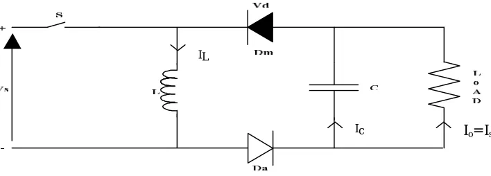
There are various topologies in the context of dc-dc converters the buck-boostFig. 1 Schematic diagram of non-isolated buck-boost converter
II. OPERATIONAL CIRCUIT FOR BUCK-BOOST CONVERTER
The circuit operation divided into two modes.
Mode 1 (Switch is closed): When switch is closed then diodes D and D are reverse biased. The input current, which rises, flows through inductor L and switch S. This results accumulating energy in inductor L. The capacitor C discharges through load R.
Fig.2 Operating mode condition of non-isolated buck-boost converter when switch is closed
Mode 2 (Switch is open): When switch is open then the current, which was flowing through inductor L, would flow
through L, C, D , D and the load. The energy stored in inductor L would be transferred to the capacitor and load,
inductor current would fall until transistor switch Q is switched on again in the next cycle.
Fig. 3 Operating mode condition of non-isolated buck-boost converter when switch is open
Io= Is
Ic
Ic Io= Is
1
( )
, 0 , :
1
( )
L
in
o o
di
V dt L
t dT Q ON dv v
dt C R
and when the switch is OFF
1 ( )
, , :
1
( )
L o
o o
L
di v
dt L
dT t T Q OFF
dv v
i
dt C R
In this Buck-Boost converter we have assume that the output voltage Vout = 400V. A simple Buck-Boost converter
realize in MATLAB Simulink is shown in fig. 4.
Fig. 4 A simple Buck-Boost converter realize in Simulink
Design parameters and equations for non-isolated Buck-Boost Converter
Parameter Design Equations
Output Voltage
=
/(1
−
)
Inductor
= (1
−
) /(
∆
)
Capacitor
= /{(
)(
∆
⁄
)}
Calculated value of design variables are L= 54.48 mH, C= 1.1248 µF and D= 0.5624.
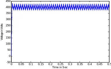
Fig. 5 Open loop response of Buck-Boost converter
AC C
v +
-Universal Bridge A
B +
- R Scope
Pulse Generator
Mosfet g m D S
L
i
+
-C
0 0.05 0.1 0.15 0.2 0.25 0.3 0.35 0.4 0.45 0.5 -50
0 50 100 150 200 250 300 350 400 450
Time in Sec
V
o
lt
a
g
e
i
n
V
o
lt
The results of open loop Buck-Boost converter is shown in figure 5, which depict peak to peak ripple voltage (ΔVo) is
54 Volt and maximum overshoot of 10%.
CLOSED LOOP BUCK-BOOST CONVERTER
The Simulink Schematic of Buck- Boost converter with analog PI controller is shown in fig. 6
Fig. 6 Simulink model of Closed loop Buck-Boost converter
The output voltage is sensed and compared with the input voltage and produce an error signal which is sent to
the PI controller to generate a control voltage . The control voltage in turn to feed to the PWM generator which alters
the duty cycle. The PI controller have two parameters namely , . These two terms can take any real value and
finding these values by different method are collectively called as PI tuning.
The PI Algorithm C = K e + K ∫e dt Where
C = Controller output signal.
e (t) = Current controller error.
K : = Proportional Gain.
K : = Integral Gain.
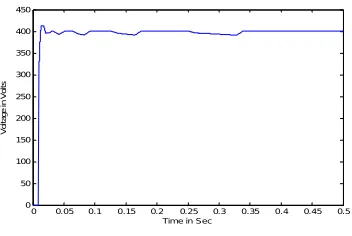
Fig. 7 Closed loop Buck-Boost Converter response
The results of closed loop Buck-Boost converter is shown in figure 7 for KP= 0.0002 and KI= 0.029, which depict
maximum overshoot of 3.25%, settling time 0.02ms and rise time 0.011ms.
AC voltage C C +v
-Universal Bridge A
B +
-Scope
PWM In1
Out1 Out2 Out3 Mosfet
g D
S
Discrete PI Controller
PI
i
+
-Constant 400
0 0.05 0.1 0.15 0.2 0.25 0.3 0.35 0.4 0.45 0.5 0
50 100 150 200 250 300 350 400 450
Time in Sec
V
o
lt
a
g
e
i
n
V
o
lt
III.EFFECTDUETOVARIATIONOFKP AND KIONOUTPUTVOLTAGEANDINDUCTORCURRENT
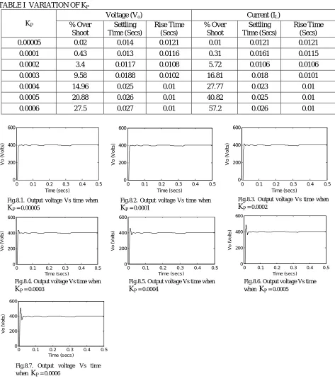
TABLE I VARIATION OF KP
KP
Voltage (Vo) Current (IL)
% Over Shoot
Settling Time (Secs)
Rise Time (Secs)
% Over Shoot
Settling Time (Secs)
Rise Time (Secs)
0.00005 0.02 0.014 0.0121 0.01 0.0121 0.0121
0.0001 0.43 0.013 0.0116 0.31 0.0161 0.0115
0.0002 3.4 0.0117 0.0108 5.72 0.0106 0.0106
0.0003 9.58 0.0188 0.0102 16.81 0.018 0.0101
0.0004 14.96 0.025 0.01 27.77 0.023 0.01
0.0005 20.88 0.026 0.01 40.82 0.025 0.01
0.0006 27.5 0.027 0.01 57.2 0.026 0.01
Fig.8. Effect on output voltage due to variation in KP
0 0.1 0.2 0.3 0.4 0.5 0
200 400 600
Time (secs)
V
o
(
V
o
lt
s
)
0 0.1 0.2 0.3 0.4 0.5 0
200 400 600
Time (secs)
V
o
(
V
o
lt
s
)
0 0.1 0.2 0.3 0.4 0.5 0
200 400 600
Time (secs)
V
o
(
V
o
lt
s
)
0 0.1 0.2 0.3 0.4 0.5
0 200 400 600
Time (secs)
Vo
(
Vo
lt
s
)
0 0.1 0.2 0.3 0.4 0.5
0 200 400 600
Time (secs)
V
o
(
V
o
lts
)
0 0.1 0.2 0.3 0.4 0.5
0 200 400 600
Time (secs)
V
o
(
V
o
lt
s
)
0 0.1 0.2 0.3 0.4 0.5 0
200 400 600
Time (secs)
V
o
(
V
o
lt
s
)
Fig.8.1. Output voltage Vs time when
KP = 0.00005
Fig.8.2. Output voltage Vs time when
KP = 0.0001
Fig.8.3. Output voltage Vs time when
KP = 0.0002
Fig.8.4. Output voltage Vs time when
KP = 0.0003
Fig.8.5. Output voltage Vs time when
KP = 0.0004
Fig.8.6. Output voltage Vs time when KP = 0.0005
When the value of K increases up to three times of the designed values then output voltage overshoot and settling
time continuously increases however rise time continuously decreases and finally attain a constant value. If value of K
decreases from its designed value then output voltage overshoot decreases however settling time and rise time increases.
Fig.12. Effect on inductor current due to variation in Kp
0 5 10 15 20 25 30
0 0.0005 0.001
% O v er sh o o t Kp 0 0.005 0.01 0.015 0.02 0.025 0.03
0 0.0005 0.001
S et tl in g T im e (S ec s) Kp 0 0.005 0.01 0.015
0 0.0005 0.001
Ri se T im e (S ec s) Kp
0 0.1 0.2 0.3 0.4 0.5
0 1 2 3 Time (secs) IL ( A m p e re )
0 0.1 0.2 0.3 0.4 0.5
0 1 2 3 Time (secs) IL ( A m p e re )
0 0.1 0.2 0.3 0.4 0.5
0 200 400 600 Time (secs) IL (A m p e re )
0 0.1 0.2 0.3 0.4 0.5
0 1 2 3 Time (secs) IL ( A m p e re )
0 0.1 0.2 0.3 0.4 0.5
0 1 2 3 4 Time (secs) IL ( A m p e re )
0 0.1 0.2 0.3 0.4 0.5 0 1 2 3 4 Time (secs) IL ( A m p e re )
0 0.1 0.2 0.3 0.4 0.5
0 1 2 3 4 Time (secs) IL ( A m p e re )
Fig.9. Effect on overshoot due to variation in KP
Fig.10. Effect on settling time due to variation in KP
Fig.11. Effect on rise time due to variation in KP
Fig.12.4. Output current Vs time when Kp= 0.0003
Fig.12.2. Output current Vs time when Kp= 0.0002
Fig.12.5. Output current Vs time when Kp= 0.0004
Fig.12.6. Output current Vs time when Kp= 0.0004
Fig.12.7. Output current Vs time when Kp= 0.0004 Fig.12.1. Output current Vs time when
Kp= 0.0002
When the value of K increases three times of the designed values then inductor current (I ) overshoot and settling
time continuously increases however rise time continuously decreases and finally attain a constant value. If value of K
decreases from its designed value then inductor current (I ) overshoot decreases however settling time and rise time
increases.
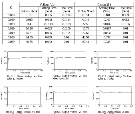
TABLE IV. VARIATION OF KI
KI
Voltage (Vo) Current (IL)
% Over Shoot
Settling Time (Secs)
Rise Time
(Secs) % Over Shoot
Settling Time (Secs)
Rise Time (Secs)
0.009 0.01 0.185 0.0124 0.014 0.181 0.179
0.019 0.015 0.045 0.0114 0.019 0.042 0.012
0.029 3.4 0.0118 0.0108 5.72 0.0106 0.0106
0.039 10.26 0.023 0.0109 17.75 0.0187 0.01
0.049 15.81 0.035 0.0104 27.65 0.0336 0.01
0.059 24.50 0.039 0.01 43.92 0.037 0.01
0.069 30.85 0.042 0.01 57.41 0.038 0.01
0 10 20 30
0 0.0005 0.001
% O v er sh o o t Kp 0 0.01 0.02 0.03
0 0.0005 0.001
S et tl in g T im e (S ec s) Kp 0 0.005 0.01 0.015
0 0.0005 0.001
Ri se T im e (S ec s) Kp
0 0.1 0.2 0.3 0.4 0.5 0 200 400 600 V o ( V o lt s ) Time (secs)
0 0.1 0.2 0.3 0.4 0.5 0 200 400 600 Time (secs) V o ( V o lt s )
0 0.1 0.2 0.3 0.4 0.5 0 200 400 600 Time (secs) V o ( V o lt s )
0 0.1 0.2 0.3 0.4 0.5 0 200 400 600 Time (secs) V o ( V o lt s )
0 0.1 0.2 0.3 0.4 0.5 0 200 400 600 Time (secs) V o ( V o lt s )
0 0.1 0.2 0.3 0.4 0.5 0 200 400 600 Time (secs) V o ( V o lt s )
Fig.13. Effect on overshoot due to variation in KP
Fig.14. Effect on settling time due to variation in KP
Fig.15. Effect on rise time due to variation in KP
Fig.16.3. Output voltage Vs time when KI = 0.029
Fig.16.1. Output voltage Vs time when KI = 0.009
Fig.16.2. Output voltage Vs time when KI = 0.019
Fig.16.4. Output voltage Vs time when KI = 0.039
Fig.16.6. Output voltage Vs time when KI = 0.059
Fig.16. Effect on output voltage due to variation in KI
When the value of K increases up to two times of the designed value then output voltage overshoot and settling time
continuously increases however rise time continuously decreases and finally attain a constant value. If value of K
decreases from its designed value then output voltage overshoot decreases however settling time and rise time increases.
0 0.1 0.2 0.3 0.4 0.5
0 200 400 600 Time (secs) V o ( V o lt s ) -10 0 10 20 30 40
0 0.05 0.1
% O v er S h o o t KI 0 0.2 0.4 0.6
0 0.05 0.1
S et tl in g T im e (S ec s) KI 0 0.005 0.01 0.015
0 0.05 0.1
Ri se T im e (S ec s) KI
0 0.1 0.2 0.3 0.4 0.5 0 1 2 3 Time (secs) IL ( A m p e re )
0 0.1 0.2 0.3 0.4 0.5 0 1 2 3 Time (secs) IL ( A m p e re )
0 0.1 0.2 0.3 0.4 0.5 0 1 2 3 Time (secs) IL ( A m p e re )
0 0.1 0.2 0.3 0.4 0.5 0 1 2 3 Time (secs) IL ( A m p e re )
0 0.1 0.2 0.3 0.4 0.5 0 1 2 3 4 Time (secs) IL ( A m p e re )
0 0.1 0.2 0.3 0.4 0.5 0 1 2 3 4 Time (secs) IL ( A m p e re )
Fig.16.7. Output voltage Vs time when KI = 0.069
Fig.17. Effect on overshoot due to variation in KI
Fig.18. Effect on settling time due to variation in KI
Fig.19. Effect on rise time due to variation in KI
Fig.20.1. Output current Vs time when KI = 0.009
Fig.20.2. Output current Vs time when KI = 0.019
Fig.20.3. Output current Vs time when KI = 0.029
Fig.20.4. Output current Vs time when KI = 0.039
Fig.20.5. Output current Vs time when KI = 0.049
When the value of K increases up to two times of the designed value then inductor current (I ) overshoot and settling
time continuously increases however rise time continuously decreases and finally attain a constant value. If value of K
decreases from its designed value then inductor current (I ) overshoot decreases however settling time and rise time
increases.
IV. CONCLUSION
DC-DC converters and their design remain an interesting topic and new control schemes to achieve better regulation and fast transient response are continually developed. Step up switching regulators are the backbone of power electronic equipments. A key challenge to design switching regulators is to maintain almost constant output voltage within acceptable regulation. Performance and applicability of this converter is presented on the basis of simulation in MATLAB SIMULINK. The design concepts are validated through simulation and results obtained show that a closed loop system using buck-boost converter will be highly stable with high efficiency. Buck-Boost converter can be used for universal input voltage and wide output power range. The design of DC-DC converter capable of having low rise time, quick settling time and stable output.
REFERENCES
[1] Robert W. Erickson and Dragan Makshnovic, “Fundamental of Power Electronics”, Second Edition, Lower Academic Publishers, New York 2004.
[2] Xu Zhang, “Digital Control Techniques for DC-DC Synchronous Buck Converter?, Doctor of Philosophy Thesis, Department 0f Electrical and Computer Engineering, UMI 3403995, ProQuest LLC, 2010.
[3] S. C. Raviraj and P. C. Sen, “Comparative study of proportional-integral, sliding mode, and flay logic controllers for power converters,” IEEE Transactions on Industrial Applications, vol 33, no.2, pp.518— 524, MariApr. 1997.
[4] M. Namnabat, M. Baysti Poodeh, S. Eshlehardiha, “Comparison the Control Methods in Improvement the Performance of the DC-DC Converter”, The 7’ international conference on power electronics, 22- 26, EXCO, Daegu, Korea, 2007.
[5] Sanjeev Singh and Bhim Singh, “Power quality improved PMBLDCM drive for adjustable speed application with reduced sensor buck-boost PFC converter” in proc. IEEE 11th ICETET, 2011, pp.180-184
[6] Sanjeev Singh and Bhim Singh, “Comprehensive study of single-phase AC-DC power factor corrected converters with high-frequency isolation” IEEE Trans. on Industrial Informatics, vol. 7, no. 4, Nov. 2011, , pp. 540-556.
[7] Siew-Chong Tan Y. Mi. Lal Martin K. H. Cheung Clii K. Tse, “On the Practical Design of a Sliding Mode Voltage Controlled Buck Converter”,IEEE Transactions On Power Electronics, VoL 20, No.2, March 2005.
0 0.1 0.2 0.3 0.4 0.5
0 1 2 3 4
Time (secs)
IL
(
A
m
p
e
re
)
-50 0 50 100
0 0.05 0.1
%
O
v
er
S
h
o
o
t
KI
0 0.05 0.1 0.15 0.2
0 0.05 0.1
S
et
tl
in
g
T
im
e
(S
ec
s)
KI
-0.05 0 0.05 0.1 0.15 0.2
0 0.05 0.1
Ri
se
T
im
e
(S
ec
s)
KI
Fig.20.7. Output current Vs time when KI = 0.069
Fig.20. Effect on inductor current due to variation in KI
Fig.21. Effect on overshoot due to variation in KI
Fig.22. Effect on settling time due to variation in KI
[8] Altamir Ronsani and Ivo Barbi, “Three-phase single stage AC-DC buck-boost converter operating in buck and boost modes” in Proc. IEEE, 2011, pp.176-182..
[9] Venkstarsmanan, A. Sabanoivc, and S. Culç “Sliding mode control of dc-to-dc converters,” in Proc. IEEE ConE Industrial Electronics, Control Instnjmentations (IECON), pp. 25 1-258, 1985.
[10] Boopathy.K and Dr.Bhoopathy Bagan .K, ―Buck Boost converter with improved transient response for low power applications‖ in Proc. IEEE
SIEA, Sep 2011, pp. 155-160.
[11] B. Singh, B. N. Singh, A. Chandra, K. Al-Haddad, A. Pandey and D. P.Kothari, “A review of single-phase improved power quality AC-DC converters,” IEEE Trans. Industrial Electron., vol. 50, no. 5, pp. 962 – 981, Oct. 2003.
[12] N. Mohan, T. M. Undeland and W. P. Robbins, “Power Electronics: Converters, Applications and Design,” John Wiley and Sons Inc, USA,1995.