Implementation on FPGA Area-Delay
Efficient Architecture of CSLA
M. D. Bobade
1, M. N. Kakatkar
2PG Student [Electronics], Dept. of E&TC, Sinhgad College of Engineering, Pune, Maharashtra, India 2
Asst. Professor, Dept. of E&TC, Sinhgad College of Engineering, Pune, Maharashtra, India 1
ABSTRACT: In the design of VLSI, area and delay is play important role and the field of VLSI less delay and low area is required adder unit in data processing processor for performing fast arithmetic operation. Architecture of CSLA, there is chance to reduce area & delay which is based on sum generation unit and carry generation unit. In this paper 128bit, 64bit, 32bit, 16bit conventional CSLA, modified CSLA and Proposed CSLA architecture have been implemented on FPGA and compared result in term area that is of count of gate and delay. The proposed design has reduced area and delay. This work has showed the performance of the proposed design in term of delay and area. ISim simulator is used for simulating the CSLA and synthesized using Xilinx ISE design suit 14.7 then implementation is done on in virtex7 FPGA kit.
KEYWORDS: FPGA, CSLA, VLSI, Binary to excess converter (BEC), sum generation unit, carry generation unit(CG), selection unit.
I. INTRODUCTION
Area-Delay efficient and good performance VLSI systems are widely used in mobile & electronics portable devices. In arithmetic operations adder is a fundamental unit. Advanced digital signal processing & communication system involves several adder will improve performance of complex DSP system. There are different types of adder but RCA is simple design and disadvantage of RCA is more carry propagation delay. The problem of carry propagation delay in RCA is improved by independent generating carries. A carry select adder is divided into sector each perform two addition in parallel , one assuming a carry in of zero and other a carry in of 1. Conventional CSLA has less propagation delay than RCA but in the architecture of conventional CSLA uses two RCA. Proposed CSLA is avoiding the dual RCA [3]. Another modified SQRT CSLA using BEC-1 and Selection unit. It reduces the area but slightly increasing the delay[4]. In both architecture conventional CSLA and modified SQRT CSLA area is increased when number of bit increases. We did analysis on logic operation involved in conventional CSLA & modified SQRT CSLA, we find there is chance to reduce area to modifying the architecture of CSLA. Proposed CSLA based on sum generation unit, carry generation unit and selection unit is involves less logic resources and propagation delay than the conventional CSLA and modified SQRT CSLA.
In Existing CSLA there are two types of CSLA Conventional CSLA and BEC based CSLA. Conventional CSLA consist of dual RCA configuration which generates a pair of sum words and output-carry bits corresponding the i/p carry (cin= 0 and 1), and selects one out of each pair for final-sum and final-output-carry. Conventional CSLA required more area than proposed system, but the design is not attractive, since it uses dual RCA. The BEC-based CSLA consist of one RCA and BEC -1 which replaced by RCA. The BEC unit receives FS0 and FC0 output from the RCA and n bit RCA replaced by n+1 bit BEC. The most significant bit (MSB) of BEC represents Cout in which n least significant bits (LSBs) represent sum. BEC based CSLA requires less logic resources than the conventional CSLA, but it has slightly higher delay than conventional CSLA.
III
.
LOGIC EXPRESSIONA. Conventional CSLA
The structure of conventional CSLA as shown in fig. 1 conventional CSLA consist of dual SCG unit and carry & sum selection unit, two n bit i/p is applied to SCG unit. SCG consist of dual ripple carry adders RCA-1 for carry 0 and RCA-2 for carry 1.
RCA-1
RCA-2
SUM & CARRY SELECTION UNIT
A (n bit) B (n bit)
0
1
Cin
SUM Cout
Fig.1. Conventional CSLA
Logic expressions of RCA-1 and RCA-2 of the Sum and Carry Generation unit of the n-bit CSLA are given as below.
Consider two n-bit operands are added in the conventional CSLA, then RCA-1 and RCA-2 generates n-bit sum FS0 and FS1, carry FC0 & FC1 corresponding to i/p carry (Cin=0 & Cin=1) respectively.
B. BEC based CSLA
The structure of BEC based CSLA as shown in fig. 2 conventional CSLA consist of single RCA and BEC-1. In the conventional CSLA RCA-2 is replaced by BEC-1 (binary to excess one converter) in order to reduce area and power consumption. Two n-bit inputs applied to RCA-1 and output of RCA-0 is as input of BEC-1 unit hence n-bit RCA-1 is replaced by (n+1) bit BEC-1. Construction ripple carry adder is same as mentioned in conventional CSLA. Logic expressions of RCA-1 and BEC-1 of BEC based CSLA are given as below. Consider two n-bit operands are added in the BEC based CSLA, then RCA-1 a generate n-bit sum FS0 and FC0 and BEC-1 can generate carry FS1 & FC1. We can find from logic expression of BEC based CSLA, carry FC1 depends on FS0, which otherwise has no dependence on FS0 in the case of conventional CSLA. BEC method increases data dependence in the CSLA.
RCA
BEC UNIT
SUM & CARRY SELECTION UNIT
A (n bit) B (n bit)
0
Cin
SUM Cout
Fig.2. BEC based CSLA
III
.
PROPOSED CSLA DESIGNThe proposed CSLA design is based on the logic expressions given as below, and its design structure is shown in Fig. 3. We find that large amount of logic resources is used for calculating FS0 and FS1 in conventional and BEC based CSLA. It is not an efficient approach to reject one sum word after the calculation. Instead of that to select one carry word from two carry word corresponding „0‟ and „1‟ to calculate final sum. Using this method, we can have three advantages calculation of FS0 is not required, n-bit selection unit required than n+1 bit and small output carry delay is required. It consists of one HSG (half sum generation unit), one HCG (half carry generation unit) , one FSG (full sum generation unit), one CG (Carry generation unit), and one CS (Carry selection unit). The CG unit consist of CG0 & CG1, CG0 is carry generation unit to i/p carry‟0‟ & CG1 for i/p carry „1‟. Two n-bit i/p data (A & B) are applied to HSG unit will generate half sum word(HS) and half carry(HC) . both CG0 & CG1 receives HS and HC from HSG unit and generate two n bit FC0 & FC1 words corresponding to i/p carry „1‟ & „0‟ respectively. The carry select unit basically consist of AND- OR gate and the gate level design of CG, HSG and CS, as shown in fig. 3. The carry select unit select one carry word from two carry word which generated by CG unit.
HSG & HCG CG0 CG1 CS UNIT FSG UNIT Cin A (n bit)
B (n bit)
Sum (n bit) Cout
Fig. 3 Proposed System.
Logic expressions of proposed CSLA are given as below.
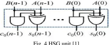
A. HSG Unit:
The logic diagram of the HSG unit is shown in Fig. 4. It consist of Combinational Logical AND Gate and OR Gate.
Fig. 4 HSG unit [1]
B. CG0 & CG1 Unit
The logic circuits of CG0 and CG1 are optimized to take advantage of the fixed input-carry bits. The optimized designs of CG0 and CG1 are shown in Fig. 5. It Consist of logical or and logical and gates.
Fig. 5 CG0 & CG1 Unit [1]
C. CS Unit
CS Unit is referred as Carry Select unit and it consist of combination of logical OR and Logical AND gates as shown in fig. 6. The CS unit selects one final carry word from the two carry words available at its input line using the control signal cin. It selects FC0 when cin = 0; otherwise, it selects FC1. The CS unit can be implemented using an n-bit 2-to-l MUX. The final carry word C(i) is obtained from the CS unit. The MSB of C(i) is sent to output as Cout, and (n − 1) LSBs are XORed with (n − 1) MSBs of half-sum (s0) in the FSG[shown in Fig. 6 to obtain (n − 1) MSBs of final-sum (s). The LSB of s0 is XORed with cin to obtain the LSB of s.
Fig. 6 CS Unit[1]
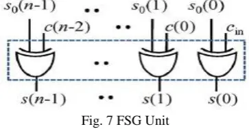
D. FSG Unit
Fig. 7 FSG Unit
IV. FPGA IMPLEMENTATION RESULT
We have coded logic expression of Proposed CSLA, BEC based CSLA and conventional CSLA in verilog-HDL for 8-bit, 16-8-bit, 32-8-bit, 64-bit and 128-bit. ISim simulator is used for simulating the CSLA and synthesized using Xilinx ISE design suit 14.7 then implementation is done on in virtex7 FPGA kit. The synthesis result of 8-bit, 16-bit, 32-bit, 64-bit and 128-bit is given in Table I as shown in below.
TABLE I
COMPARISION OF PROPOSED CSLA AND EXIXTING CSLA ON AREA COUNT No bit\
area
Conventional CSLA
BEC-based CSLA
Proposed CSLA
8 bit 202 165 80 16 bit 538 333 160 32 bit 859 669 350 64 bit 1714 1341 640 128 bit 3442 2685 1280
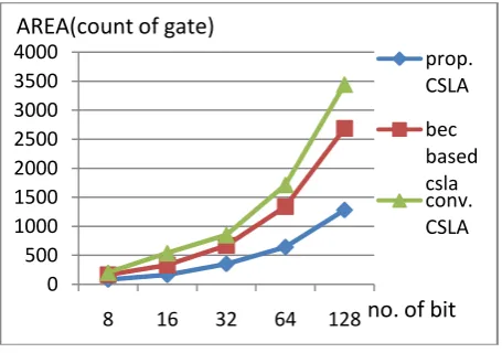
Comparison of CPD (carry propagation delay) of 8-bit, 16-bit, 32-bit, 64-bit and 128-bit as shown in Table II and we plot graphs area (gate count) verses no. of bit size and CPD vs. No. of bit size for Proposed CSLA, BEC based CSLA and conventional CSLA, hence we can easily observe that the proposed CSLA is require less area-delay than existing CSLA.
TABLE II
COMPARISION OF PROPOSED CSLA AND EXIXTING CSLA ON DELAY
According to synthesis result on Xilinx 14.7 we measured CPD for proposed CSLA, BEC based CSLA and Conventional CSLA for 8-bit, 16-bit, 32-bit, 64-bit, 128-bit. We plotted graph between delay and no of bit for existing system and proposed CSLA as shown in fig 8.
No of bits\ Delay (ns)
Conventional CSLA
BEC-based CSLA
Propose d CSLA
8 bit 2.535 3.160 2.485
16 bit 5.402 5.907 4.070
32 bit 7.980 10.398 7.238
64 bit 15.239 20.047 13.576
Fig. 8 Comparison of Delay for Proposed CSLA and Existing CSLA
We synthesized proposed CSLA, conventional CSLA and BEC based CSLA on Xilinx 14.7. we observed that logic resources require for proposed CSLA less than existing CSLA that plotted on graph which shown in fig. 10.
Fig. 9 Comparison of Area for Proposed CSLA and Existing CSLA
Fig. 10 shows the RTL schematic of 128 bit proposed CSLA An even higher level describes the registers and the transfers of vectors of information between registers. This is called the Register Transfer Level (RTL). Verilog supports all of these levels. However, this handout focuses on only the portions of Verilog which support the RTL level.
Fig. 10 RTL schematic of 128 bit proposed CSLA. 0
10 20 30 40 50
8 16 32 64 128
prop. CSLA
bec based csla conv. CSLA
no. of bit csla
Delay in ns
0 500 1000 1500 2000 2500 3000 3500 4000
8 16 32 64 128
prop. CSLA
bec based csla conv. CSLA
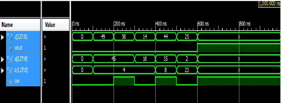
We simulated proposed CSLA for 128 bit. First i/p „a‟ of 128 bit and second i/p „b‟ of 128 bit cin for input carry and sum value represented by s(127:0) bit and cout represent final carry as shown in fig 11. We gave unsigned decimal input as a=45, b=4,cin=1 then we can observed simulation result sum=50, cout=0 on fig. 11.
Fig. 11 simulation result of 128 bit proposed CSLA.
V. CONCLUSIONS
We have analysed the logic expression which is included in conventional CSLA and BEC based CSLA. We find that there are redundant logic operation involved in exiting system and data dependence. Proposed CSLA eliminated all redundant logic expression of conventional CSLA and BEC based CSLA. In the proposed CSLA carry selection operation scheduled before the calculating final sum which different approach from conventional CSLA. From Table I, we can conclude that proposed CSLA require less number of gate than existing CSLA for 8-bit, 16-bit, 32-bit, 64-bit, 128-bit. From Table II, we can conclude that proposed CSLA has less CPD than existing CSLA for 8-bit, 16-bit, 32-bit, 64-bit, 128-bit. Hence The proposed SQRT-CSLA involves significantly less area and less delay than the existing designs. Proposed SQRT-CSLA architecture is 52.32% more efficient than BEC based CSLA and 62.81% more efficient than conventional based CSLA in terms of area for 128 bit. Delay has been reduced by 29.55% than BEC based CSLA and 11.85% than Conventional CSLA for 128 bit.
REFERENCES
[1] Basant Kumar Mohanty, Senior Member, IEEE, and Sujit Kumar Patel “Area-Delay-Power Efficient Carry Select Adder” IEEE Transaction On Circuit And System –Ii Express Briefs. Vol. 61. No.6, June 2014.
[2] B. Ramkumar, H.M. Kittur, and P. M. Karman, "Low-Power and Area-Efficient Carry select adder "IEEE Transactions on Very Large Scale Integration System, Vol.20, No.2, February 2012
[3] B. Ramkumar, H.M. Kittur, and P. M. Karman, "ASIC implementation of modified faster carry save adder, " Eur. J. Sci. Res., vol. 42, no. 1, pp.53-58, MAY 2010.
[4] T. Y. Ceiang and M. 1. Hsiao, "Carry-select adder using single ripple Carry adder, " Electron. Lett, vol. 34, no. 22, pp. 2101-2103, Oct. 1998. [5] Y. Kim and L.-S. Kim, "64-bit carry-select adder with reduced area, " Electron. Lett. vol. 37, no. 10, pp. 614- 615, May 2001.
[6] Y. He, C. H. Chang, and J. Gu, "An area efficient 64- Bit square Root carry-select adder for low power Applications, " in Proc. IEEE Int. Symp.Circuits Syst., vol. 4, pp. 4082-4085, 2005.
[7] A. P. Chandrakasan, N. Verma, and D. C. Daly, “Ultralow-power electronics for biomedical applications,” Annu. Rev. Biomed. Eng., vol. 10, pp. 247–274, Aug. 2008.
[8] O. J. Bedrij, “Carry-select adder,” IRE Trans. Electron. Comput., vol. EC-11, no. 3, pp. 340–344, Jun. 1962.
[9] Y. Kim and L.-S. Kim, “64-bit carry-select adder with reduced area,” Electron. Lett., vol. 37, no. 10, pp. 614–615, May 2001.
![Fig. 5 CG0 & CG1 Unit [1]](https://thumb-us.123doks.com/thumbv2/123dok_us/7786805.1288517/5.595.177.429.202.428/fig-cg-cg-unit.webp)