Logic Foundry: Rapid Prototyping for FPGA-Based
DSP Systems
Gary Spivey
Rincon Research Corporation, Tucson, AZ 85711, USA Email:[email protected]
Shuvra S. Bhattacharyya
Electrical and Computer Engineering Department and UMIACS, University of Maryland, College Park, MD 20742, USA Email:[email protected]
Kazuo Nakajima
Electrical and Computer Engineering Department, University of Maryland, College Park, MD 20742, USA
New Architecture Open Lab, NTT Communication Science Labs, Kyoto, Japan Email:[email protected]
Received 13 March 2002 and in revised form 9 October 2002
We introduce the Logic Foundry, a system for the rapid creation and integration of FPGA-based digital signal processing sys-tems. Recognizing that some of the greatest challenges in creating FPGA-based systems occur in the integration of the various components, we have proposed a system that targets the following four areas of integration: design flow integration, component integration, platform integration, and software integration. Using the Logic Foundry, a system can be easily specified, and then automatically constructed and integrated with system level software.
Keywords and phrases:FPGA, DSP, rapid prototyping, design methodology, CAD tools, integration.
1. INTRODUCTION
A large number of system development and integration com-panies, labs, and government agencies (hereafter referred to as “the community”) have traditionally produced digital sig-nal processing applications requiring rapid development and deployment as well as ongoing design flexibility. Frequently, these demands are such that there is no distinction between the prototype and the “real” system. These applications are generally low-volume and frequently specific to defense and government requirements. This task has generally been per-formed by software applications on general-purpose com-puters. Often these general-purpose solutions are not ade-quate for the processing requirements of the applications, and the designers have been forced to employ solutions in-volving special-purpose hardware acceleration capabilities.
These special-purpose hardware accelerators come at a significant cost. The community does not possess the large infrastructure or volume requirements necessary to pro-duce or maintain special-purpose hardware. Additionally, the investment made in integrating special-purpose hard-ware makes technology migration difficult in an
environ-ment where utilization of leading-edge technology is criti-cal and often pioneered. Recent improvements in Field Pro-grammable Gate Array technology have made FPGA’s a vi-able platform for the development of special-purpose digi-tal signal processing hardware [1], while still allowing design flexibility and the promise of design migration to future tech-nologies [2]. Many entities within the community are eyeing FPGA-based platforms as a way to provide rapidly deploy-able, flexible, and portable hardware solutions.
Introducing FPGA components into DSP system imple-mentations creates an assortment of challenges across sys-tem architecture and logic design. Where syssys-tem architects may be available, skilled logic designers are a scarce resource. There is a growing need for tools to allow system architects to be able to implement FPGA-based platforms with lim-ited input from logic designers. Unfortunately, getting de-signs translated from software algorithms to hardware im-plementations has proven to be difficult.
description language (HDL) format such as Verilog HDL or VHDL that can be processed by traditional FPGA design flows. Other tools use derived languages based on C such as Handel-C [4], C++ extensions such as SystemC [5], or Java classes such as JHDL [6]. These tools give designers the abil-ity to more accurately model the parallelism offered by the underlying hardware elements. While these approaches at-tempt to raise the abstraction level for design entry, many experienced logic designers argue that these higher levels of abstraction do not address the underlying complexities re-quired for efficient hardware implementations.
Another approach has been to use “block-based design” [7] where system designers can behaviorally model at the sys-tem level, and then partition and map design components onto specific hardware blocks which are then designed to meet timing, power, and area constraints. An example of this technique is the Xilinx system generator for the mathworks simulink interface [8]. Using this tool, a system designer can develop high-performance DSP systems for Xilinx FPGA’s. Designers can design and simulate a system using Matlab, Simulink, and a Xilinx library of bit/cycle-true models. The tool will then automatically generate synthesizable HDL code mapped to Xilinx pre-optimized algorithms [8]. However, this block-based approach still requires that the designer be intimately involved with the timing and control aspects of cores in addition to being able to execute the back-end pro-cesses of the FPGA design flow. Furthermore, the only blocks available to the designer are the standard library of Xilinx IP cores. Other “black-box” cores can be developed by a logic designer using standard HDL techniques, but these cannot currently be modeled in the same environment. Annapolis MicroSystems has developed a tool entitled “CoreFire” that uses prebuilt blocks to obviate the need for the back-end processes of the FPGA design flow, but is limited in applica-tion to Annapolis MicroSystems hardware [9]. In both of the above cases, the system designer must still be intimate with the underlying hardware in order to effectively integrate the hardware into a given software environment.
Some have proposed using high-level, embedded system design tools, such as Ptolemy [10] and Polis [11]. These tools emphasize overall system simulation and software synthe-sis rather than the details required in creating and integrat-ing FPGA-based hardware into an existintegrat-ing system. An effort funded by the DARPA adaptive computing systems (ACS) was performed by Sanders (now BAE Systems) [12] that was successful in transforming an SDF graph into a reason-able FPGA implementation. However, this effort was strictly limited to the implementation of a signal processing data-path with no provisions for runtime control of processing elements. Another ACS effort, Champion [13], was imple-mented using Khoros’s Cantata [14] as a development and simulation environment. This effort was also limited to dat-apaths without runtime control considerations. While data-path generation is easily scalable, control synthesis is not. In-creased amounts of control will rapidly degrade system tim-ing, often to the point where the design becomes unusable.
In the above brief survey of relevant work, we have ob-served that while some of these efforts have focused on the
design of FPGA-based DSP processing systems, there has been less work in the area of implementing and integrat-ing these designs into existintegrat-ing software application environ-ments. Typically a specific hardware platform has been tar-geted, and integration into this platform is left as a task for the user. Software front-ends are generally designed on an application-by-application basis and for specific software en-vironments. Because the community requirements are often rapidly changing and increasing in complexity, it is neces-sary for any solution to be rapidly designed and modified, portable to the latest, most powerful processing platform, and easily integrated into a variety of front-end software ap-plication environments. In other words, in addition to the challenge of creating an FPGA-based DSP design, there is an-other great challenge in implementing that design and inte-grating it into a working software application environment.
To help address this challenge, we have created the Logic Foundry. The Logic Foundry uses a platform-based design approach. Platform-based design starts at the system level and achieves its high productivity through extensive, planned design reuse. Productivity is increased by using predictable, preverified blocks that have standardized interfaces [7]. To facilitate the rapid implementation and deployment of these platform-based designs, we have identified four areas of in-tegration as targets for improvement in a rapid prototyping environment for digital signal processing systems. These four areas aredesign flow integration,component integration, plat-form integration,and software integration.
Design flow integration
In addition to standardized component development meth-odologies [15,16], we have also proposed that these prever-ified blocks be assembled with all the information required for back-end FPGA design automation. This will allow logic designers to integrate the FPGA design flow into their com-ponents. With tools we have developed as part of the Logic Foundry, a system designer can perform back-end FPGA processing automatically without any involvement with the technical details of timing and layout.
Component integration
We have proposed that any of the aforementioned pre-verified blocks, orcomponents, that are presented to the high-level system designer should consist of standardized inter-faces that we callportals. Portals are made up of a collection of data and control pins that can be automatically connected by the Logic Foundry while protecting all timing concerns. The Logic Foundry was built with the requirement that it had to handle runtime control of its components; therefore we have designed a control portal that can scale easily with the number of components in the system without adversely affecting overall system timing.
Platform integration
platforms. This can cause portability problems if the unique platform interface details have been tied deeply into the FPGA design (e.g., memory latency). Additionally, underly-ing FPGA technology changes (e.g., from Altera to Xilinx) can easily break former FPGA designs. Because of the com-munity need to frequently upgrade to the latest, most pow-erful hardware platforms, Logic Foundry components are developed in a platform-independent manner. By providing abstract interface portals for system input/output, and mem-ory accesses, designs can be easily mapped into most plat-form architectures.
Software integration
In addition to the hardware portability challenges, software faces the same issues as unique driver calls and system access methodologies become embedded deeply in the software ap-plication program. This can require an apap-plication program to be substantially rewritten for a new FPGA platform. It is also desirable to be able to make use of the same FPGA accel-eration platform from different software environments such as Python, straight C code, Matlab, or Midas 2k [17] (a soft-ware system developed by Rincon Research for digital signal processing). For example, the same application could be used in a fielded Midas 2k application as a researcher would access in a Matlab simulation. Porting the application amongst the various environments can be a difficult endeavor. In order to accommodate a wide variety of software front-ends, the Logic Foundry isolates front-end software applications envi-ronments and back-end processing envienvi-ronments through a standardized API. While other tools such as Handel-C and JHDL provide an API that allows software to abstractly in-teract with the I/O interfaces, the application must still be aware of internal hardware details. Our API, known as the DynamO API, provides dynamic object (DynamO) creation for the software front-end that completely encapsulates both I/O details and component control parameters such as reg-ister addresses and control protocols. Using the DynamO object and API, an application programmer interacts solely with the conceptual objects provided by the logic designer.
Each area of integration in the Logic Foundry can be used independently. While the Logic Foundry provides easy link-ages between all areas, a user might make use of but one area, allowing the Logic Foundry to be adopted incremen-tally throughout the community. For clarity, we will begin the Logic Foundry discussion with a design example, ex-plaining how the design would be implemented in an FPGA, and then how a software system might make use of the hard-ware implementation. Section 2introduces this design that will serve as an example throughout the paper. Sections 3
through6detail the four areas of integration, and how they are addressed by the Logic Foundry design environment.
2. DESIGN EXAMPLE
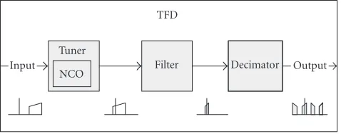
For an FPGA-based system example, we examine a signal processing system that contains atune/filter/decimate(TFD) process being performed in a general-purpose computer (see
Input
Tuner
NCO Filter
TFD
Decimator Output
Figure1: Tune/filter/decimate.
Figure 1). The TFD is a standard digital signal processing technique used to downconvert a tuned signal to baseband and often implemented in FPGA’s [18].
We would like to move the TFD functionality to an FPGA platform for processing acceleration. Inside the FPGA, the TFD block will be made up of three cores, a tuner with a modifiablefrequencyparameter, an FIR filter with reloadable taps, and a decimator with a modifiable decimationamount. Thetunercore will contain a numerically controlled oscilla-tor (NCO) core as well. The TFD will be required to interface to streaming inputs and streaming outputs that themselves interface via the pins of the FPGA to the general-purpose host computer.
The system will stream data through the TFD in blocks of potentially varying size. While this is occurring, the sys-tem may dynamically change the tune frequency, filter taps, or decimation value in both adata-asynchronousand data-synchronousmanner. We define a data-asynchronous param-eter access as a paramparam-eter access that occurs at an indparam-etermi- indetermi-nate point in the data stream. A data-synchronous parameter access occurs at a determinate point in the data stream.
The output of the TFD will be read into a general-purpose computer where software will pass the result on to other processes such as a demodulator. We would like to in-put the data from either the general-purpose comin-puter or from an external I/O port on the FPGA platform. Rather than having a runtime configurable option, we would like to be able to quickly make two different FPGA images for each case.
In our example, we assume that we will be using an An-napolis MicroSystems Starfire [19] card as an FPGA plat-form. This card has one Xilinx FPGA, plugs into a PCI bus, and is delivered with software drivers. Our systems applica-tion software will be Midas 2k [17].
3. DESIGN FLOW INTEGRATION
Tuner Filter TFD
Decimator
NCO
Figure2: MEADE node structure for the Tune/filter/decimate.
processors, the realized algorithm on an FPGA may be quite different than the algorithm originally specified by the sys-tem designer.
While many languages are being proposed as system de-sign languages (among them C++, Java, and Matlab), none of these languages perform this algorithmic translation step. A common belief in the industry is that there will always be a place for the expert in the construction of FPGA’s [20]. While an expert may be required for optimal design entry, many mundane tasks are performed in the design process using a unique set of electronic design automation (EDA) tools. It is desirable to automate many of these steps without inhibiting the abilities of the skilled logic designer.
3.1. MEADE
To more efficiently integrate FPGA designs into a user-defined EDA tool flow, we have developed MEADE—the modular, extensible, adaptable design environment [21,22]. MEADE has been implemented in Perl because of its widespread use in the community and dominant success as a glue language and text parser, two requirements for an in-tegration framework for FPGA design flows.
MEADE requires users to specify anodeto represent a design “building block.” A node can be a small function such as an adder, or a large design like a turbo decoder. Further-more, nodes can be connected to other nodes or contain other nodes, allowing for design reuse and large system def-initions. In the TFD example, nodes exist for the TFD, the tuner, thefilter, thedecimator, and theNCOwithin the tuner (seeFigure 2).
MEADE nodes are directory structures with an accom-panying database that fully describes the aspects of the node. The database is contained in a.meadesubdirectory via per-sistent Perl objects [23]. The database includes information about node elements such as HDL models and testbenches, target and included libraries, and included packages. This in-formation includes file location, any node children, and spe-cial “blackboards” that can be written and read by MEADE components for extensible requirements.
MEADE nodes also provide the ability to specify unique “builds” within a given node. Using the “build” mechanism, a node can be delivered with VHDL and SystemC
implemen-tations, or with generic, Xilinx, or Altera implementations. These builds can easily be specified by a top level so that if an Altera build is desired, the top node specifies the Altera build, and then any build that has an Altera option uses its custom Altera elements. Those elements that are generic continue to be used.
To manipulate the nodes and node information, MEADE contains an extensible set ofMEADE procedures, actions, and agents. MEADE procedures are sequences of MEADE ac-tions. A MEADE action can be performed by one or more MEADE agents. These agents are used to either perform spe-cific design flow tasks or encapsulate EDA tools. For exam-ple, a simulation procedure can be defined as a sequence of actions—make, debug setup, simulate, debug, and out-put comparison (see Figure 3). If a design house has mul-tiple different simulators, such as Mentor Graphics Model-Sim or Cadence NC-Model-Sim, or third party debuggers such as Novas Debussy, an agent for each simulator exists and is se-lectable by the user at runtime. The same holds true for any other tools (analysis, synthesis, etc.). We have currently im-plemented simulation agents for Mentor Graphics ModelSim simulator, analysis agents for ModelSim and Novas’ Debussy debugger, and synthesis agents for Synplify’s Synplicity syn-thesis tool.
MEADE provides node generation procedures that con-struct standard nodes with HDL templates for the design and testbenches. To accommodate rapid testbench construc-tion, MEADE employs a client/server testbench model [24] and supplies a group of test modules for interfacing to HDL debuggers. Design flow scripting is typically automated by MEADE, but custom tool scripts can be designed by the node designer. This information is localized to the node being de-signed by the designer building the node. When used in a larger system, the system designer does not need to know the information required to build a subnode, as that informa-tion is automatically acquired from the subnode by MEADE. This feature makes MEADE nodes very usable as methods of IP transfer between different design groups using MEADE.
3.2. EP3
While most of the flow management in MEADE can be done by tracking files and data through the MEADE agents, some processes require that files be manipulated in unique and complex manners. Additionally, this manipulation is not al-ways desirable to be done in the background in the event that the core designer may have expert custom tailoring that the agent designer cannot anticipate. In these instances, we have found that a preprocessor step is an excellent option for many of the detailed MEADE files.
Actions Make Debug
init Simulate Debug
Output Compare
Agents EP3 ModelSim ModelSim ModelSim Compare
Debussy NC-Sim Debussy
NC-Sim NC-Sim
Figure3: The MEADE simulate procedure.
impossible. To this end we developed the extensible Perl pre-processor (EP3) [25]. EP3 enables a designer to create their own directives and embed the power of the Perl language into all of their files—linking them with the node and enabling MEADE to dynamically create files for its processes. Because it is a preprocessor rather than an explicit file manipulator, the designer can easily and selectively enact or eliminate spe-cial preprocessing directives in choice files for specific agents. Originally, EP3 was designed as a Verilog HDL prepro-cessor, but as it was developed, we decided that it should be simply an extensible standard preprocessor with the ability to dynamically include directive modules (for VHDL, etc.) at compile time or in the middle of a run. EP3 scans a file, looks for directives, strips offthe delimiter, and then calls a func-tion of the same name. The standard directives are defined within the EP3 program. Library directives or user-defined directives may be loaded as Perl modules via a command line switch for inclusion at the beginning of the EP3 run. Perl sub-routines (and hence EP3 directives) may be dynamically in-cluded during the EP3 run by simply including the subrou-tine in the text of the file to be preprocessed.
EP3 has been extended to not only parse files, but also to read in specification files, build large tables of informa-tion, and subsequently do dynamic code construction based on the information. This allows for a simple template file to create a very complex HDL description with component instantiations and interconnections done automatically and with error checking.
3.3. Design flow integration example
Consider the construction of the NCO node in the TFD example. We begin by first creating a MEADE node with the command: meade node NCO. This creates a directory entitled NCO. Inside of this directory, src andsim sub-directories are created. Template source files (NCO.ep3, NCO pkg.ep3, andNCO tb.ep3) are copied from the global MEADE configuration space and modified with the new node nameNCO. Element objects for each of these files are automatically created in the node’s database. The database would also be populated with a target compilation library for the node and a standard build. The package file includes
the VHDL component specification for this entity—this def-inition is automatically included in the design file and the testbench automatically by EP3 so that component specifica-tions can be entered once rather than the several times stan-dard HDL entry requires. The testbench file includes mod-ules that provide system and data clocks, resets, and inter-faces to debuggers in a format for runtime configuration by the MEADE simulation agents.
After editing the files to create the desired VHDL compo-nent, the commandmeade makewill invoke the EP3 agent to run EP3 on the files and produce the output filesNCO.vhd, NCO pkg.vhd, andNCO tb.vhd. The make procedure is of-ten a subset of other procedures and does not necessarily have to be run independently. Entering the commandmeade sim will execute the default simulator, MentorGraphics’ ModelSim. This involves the creation of amodelsim.inifile that provides linkages to all required simulation libraries. In a low-level node such as this one, there are few libraries— however, all of the MEADE support modules that are cluded in the testbench have their libraries automatically in-cluded in themodelsim.inifile at this time. The command line (which can be quite extensive) is formed for the appro-priate options and the simulation is run. There are many op-tions that can be handled by the simulation agent, such as whether or not the simulation is to be interactive or batch mode, which debugger format is to be used for data dumps, and simulation frequency, to name a few. Simulation out-put is directed to an appropriate text outout-put files or tion dump files and managed for the user as are any simula-tion make files that are created to avoid excessive recompiles. Using similar procedures in MEADE, the node can be run through a debugger (meade analyze), or synthesized to a structural netlist (meade synthesize).
tool encapsulation intrusive and would rather work outside of MEADE when developing cores. In these cases, a finished design can be encapsulated by MEADE in a relatively simple manner.
Upon node completion, everything about the node is en-capsulated in the MEADE database. This includes such fea-tures as which files are required for simulation, which files are required for synthesis, required simulation libraries and simulation target libraries, and any subnodes that may be required by the node. When the tuner component is con-structed, a child reference to the NCO node is simply in-cluded intuner’srequired element files. When any MEADE operations are performed on thetunernode, all tool files and command lines are automatically constructed to include the directions specified in theNCOnode.
4. COMPONENT INTEGRATION
One of the challenges in rapidly creating FPGA-based sys-tems is effective design reuse. Many designers find it prefer-able to redesign a component rather than invest the time required to effectively integrate a previously designed com-ponent. As integration is typically done in the realm of the logic designer, a system designer cannot prototype a system without requiring the detailed skills of the logic designer. The Logic Foundry provides a component abstraction that makes component integration efficient and provides MEADE con-structs that allow a system designer to create prototype sys-tems from existing components.
A Logic Foundry component specifiesattributesand por-tals. If you think of a component as a black box contain-ing some kind of functionality, thenattributesare the lights, knobs, and switches on that box. Essentially, an attribute is any publicly accessible part of the component, providing state inspectors and behavioral controls.Portalsare the ele-ments on a component that provide interconnection to the outside and are made up of user-defined pins.
4.1. The attribute interface
Other attempts at component-based FPGA-based develop-ment systems have assumed that the FPGA impledevelop-mentation is simply a static data modifying piece in a processing chain [12,13]. Logic Foundry components are designed assuming that they will require runtime control and thus are speci-fied as having a single attribute interface through which all data-asynchronous control information flows. The specifi-cation of this interface is left as an implementation-specific detail for each platform (interface mapping to platforms is described inSection 5). Each FPGA in a system has exactly one controlling attribute interface and every component has exactly one attribute interface. All data-asynchronous com-munications to the components are done through this inter-face.
An attribute interface consists of an attribute bus, a strobe signal from the controlling attribute interface, and an event signal from each component. We have implemented the attribute bus with a tristate bus that traverses the
en-Strobe Event Attr bus Controlling attribute interface
Component 0 attribute interface
Component 1 attribute interface
Component 2 attribute interface
Component 3 attribute interface
Figure4: The attribute interface.
tire chip and connects each component’s attribute interface to the controlling attribute interface (seeFigure 4). Because attribute accesses are relatively infrequent and asynchronous, the attribute bus uses a multicycle path to eliminate tim-ing concerns and minimize routtim-ing resources. Ustim-ing a sim-ple incrementer component that has an input, an output, and a single amount attribute, we have effectively imple-mented a design for 1 incrementer, 10 serial incrementers, and 50 serial incrementers with no degradation in perfor-mance.
Each component in a system has a unique address in the system. The controlling attribute interface decodes this address and enables the component via a unique strobe line from the controlling attribute interface to the addressed component. These strobe lines are distributed via delay chains and are also used by the components for attribute bus synchronization. Using delay chains costs very little in an FPGA as there are typically a large number of unused reg-isters throughout a design. Data and control are multiplexed on the bus and handled by state machines in each compo-nent which provide address, control, and data buses inside each component.
Each component also has an individual event signal that is passed back to the controlling attribute interface. With the strobe and the event lines, communication can be initiated by each end of the system. This architecture elegantly han-dles data-asynchronous communication requirements for our FPGA-based processing systems.
m
Figure5: Component FIFO interface.
4.2. Data portals
Components may have any number of input/output portals, and in a DSP system, these are generally characterized by a streaming data portal. Each streaming portal is implemented using a FIFO withreadyandvalidsignals (seeFigure 5). Us-ing FIFO’s on the inputs and outputs of a component iso-lates, both the input and the output of each cell from timing concerns as all signals going to and coming from an interface are registered. This allows components to be assembled in a larger system without fear of timing restrictions arising from component loading.
By using FIFO’s to monitor data flow, flow control is au-tomatically propagated throughout the system. It is the re-sponsibility of every component to ensure that this behavior is followed inside the component. When an interface can-not accept data, the component is responsible for stopping. If the component cannot stop, then it is up to the compo-nent to handle any dropped data. In our DSP environment, each data transfer represents a sample. By using flow control on each stream, there is no need to insert delay elements for balancing stream paths—synchronization is self-timed [26]. FIFO’s are extremely easy to implement in modern FPGA’s by using the lookup table (LUT) as a small RAM component. So, rather than providing a flip-flop for each bit as a registration between components, a single LUT can be used and (in the case of the Xilinx Virtex part) a 16 deep FIFO is created. In the Virtex parts, each FIFO controller requires but four configurable logic blocks (CLB’s). In the larger FPGA’s that we are targeting, this usage of resources is barely noticeable. Control of the FIFO is performed with simple, valid, and ready signals. Whenever both valid and ready signals are active, data transitions occur.
In the TFD example, each component receives input and output FIFO’s. Note that theNCOinside of thetuner com-ponent is simply a MEADE node and not a comcom-ponent, and thus receives no FIFO’s. This allows logic designers to build components out of many subnodes, but expose only the top level component to the system designer.
4.3. The component specification file
A component is implemented as a MEADE node that con-tains a component specification file (seeFigure 6). The ponent specification file describes any attributes for a com-ponent, as well as a component’s ports and the pins that make
Attribute interface
Amount
Import Export
@attribute portal @data portal in import @data portal out export @attribute{
name => amount,
width => IMPORT DATA WIDTH length => 1,
source => BOTH, }
Figure6: The component specification file.
up those ports. In the TFD example, attributes can be de-clared of varying widths, lengths, and initial values. The at-tribute can be written by the system, the hardware, or both. Attribute addresses may be autogenerated. Because attribute ports, and streaming data in and out ports are standard for components, EP3 directives exist to construct these ports. However, any port type can be declared.
A component’s attributes can have an open-ended num-ber of parameters, includingaddress, size, depth, initial values, andwriting source(either hardware, software, or both).
The component specification file is included via EP3 in the component HDL specification. EP3 automatically gener-ates all of the attribute assignments and read statements and connects up the attribute interface. This has to be done in the actual HDL specification because synthesis tools require that all assignments to a given register occur in the same process block. Because the component author likely wants internal access to most of the created attributes, EP3 has to insert the system portion of the attributes in the same process block. This same component specification file is ultimately parsed by the top level software to describe to the system the view of the component.
It should also be noted that all attribute addresses are relative to the component. Components are individually ad-dressed by the attribute interface. In this manner, multi-ple instances of the same component can easily coexist with identical attribute addresses, but different component ad-dresses.
4.4. Component integration example
Streaming
Figure7: Streaming portals.
a component is simply a special type of MEADE node. Con-sider construction of the decimator component from the TFD example. Entering the command: meade component decimatorcreates a MEADE node entitleddecimator. In ad-dition to the node’s design and template files (which repre-sent an incrementer by default), a standard component defi-nition file is also copied into the node. This file can be edited to add or subtract any component attributes or portals.
In the case of thedecimator component, the definition file would not have to be altered as the stock definition file has an input portal, an output portal, and a single attribute entitledamount. Thedecimator.vhdfile would be edited to change the templates increment function to a decimate function. The portions of the template file that manage the attribute interface and portal FIFO instantiations would nor-mally remain unaltered as they are autogenerated via EP3 di-rectives.
The testbench template contains servers for the data por-tals as well as the attribute portal so that system level com-mands (portal writes/reads and attribute sets/gets) can be simulated easily in the testbench. While most of the bench would be unaltered, the stimulus section of the test-bench would be modified to make the appropriate attribute set/get calls and portal writes and reads.
Performing simulation or synthesis procedures on the component node is identical to the standard MEADE node. This process is simplified greatly by MEADE as the FIFO in-terconnects, attribute interfaces, and testbench modules are all automatically included as child nodes by MEADE without any intervention from the component node designer.
5. PLATFORM INTEGRATION
When designing on a particular platform, certain aspects of the component such as memory and control interfaces are often built into the design. This poses a difficulty in al-tering the design, even on the same platform. Changing a data source from an external source to direct memory access (DMA) from the PCI bus could amount to a considerable design change as memory resources and data availability are considerably altered. This problem is exacerbated by com-pletely changing platforms. However, as considerably better platforms are always being developed, it is necessary to be able to rapidly port to these platforms.
Some work has recently been undertaken in this arena as a joint venture between Wind River with their Board
Sup-port Package (BSP) and Celoxica’s platform abstraction layer (PAL) [27]. A similar methodology was undertaken by JHDL [6] with its HWSystem class. These efforts attempt to
ab-stract the I/O interfaces between a processing platform and its host software environment, allowing an application that is developed on one platform to be migrated to another plat-form. However, the issues of platform-specific I/O to desti-nations other than the host software environment and on-board memory interfaces are not specifically addressed.
To combat this problem, the Logic Foundry employs an abstract portalfor all design level interfaces. A Logic Foundry design is specified in a designnode (as opposed to a com-ponent node) withabstract portals.Design nodes represent complete designs that are platform-independent and use generic portals.Abstract portalsare connected to component portals when building a design. These abstract portals can then be mapped to a specific platform portal in what we call animplementationnode. This form of interface abstraction is common in the design of reusable software; our contribu-tion here is to develop its capabilities in the context of FPGA implementation and DSP hardware/software integration.
5.1. Abstract portal types
There are various portal types for differing needs. While new portal types can easily be developed to suit any given need, each abstract portal type requires a corresponding imple-mentation portal for every platform. For this reason, we at-tempt to reuse existing portals whenever possible. We cur-rently support three portal types: the streaming portal, the memory portal, and the block portal.
5.1.1 The streaming portal
A streaming portal is used whenever an application expects to stream data continuously. Depending on the implemen-tation, this may or may not be the case (compare an A/D converter direct input to a PCI bus input that is buffered in memory via a DMA), but the design will be able to handle a streaming input with flow control.
Streaming portals may be implemented in many diff er-ent ways—among these, a direct DMA input to the design, a direct hardware input, a gigabit Ethernet input, or a PMC bus interface. At the design level, all of these interface types can be abstracted as a streaming portal.
5.1.2 The memory portal
There are different types of memory accesses that need to be accounted for local memory, external memory, dedicated memory and an arbitered memory, dual-port varieties, and so forth. All memory portals consist of data in, data out, ad-dress, read enable, write enable, and clock pins. We provide a group of portals that build on these common characteristics.
(a)Local (on-chip) memory
For many FPGA applications, we allow the assumption that the design has access to some amount of dedicated local memory (e.g., Block RAMS in a Xilinx Virtex Part). The Logic Foundry integrates such local memories as subnodes of a design rather than memory portals as the performance and control gains are too significant to be ignored. This does not greatly affect portability as successive generations of FPGAs tend to have more local memory rather than less. Addition-ally, drastically limiting the amount of memory available to a design would likely require algorithmic changes that would render the design unportable anyway.
(b)Design external memory
In the case of the dedicated memory, it may be desirable to pipeline memory accesses so that data can be rapidly streamed with a little latency. In the case of an arbitered memory, the memory portal must follow a transaction model, holding its memory access request until acknowl-edgement is given. These two conflicting models must be merged into a single abstract memory portal. We do this by changing theread enableandwrite enablelines to read re-quest and write rere-quest lines, respectively, and adding control pins for an access acknowledgement. By using these control signals for every external memory portal, the implementa-tion will be able to map the abstract memory portals to avail-able memory resources, using arbitered or dedicated memo-ries wherever appropriate.
One issue in the memory portal is the variable width of the memory port. By specifying a width on the portal, we will currently allow mapping to a memory implementation that is as wide as or wider than specified, padding the unused bits. This can result in an inefficient use of memory when the ab-stract width is specified as 8 bits and the actual memory is 32 bits wide. In this situation, it might be desirable to pack memory words into the larger memory, however, each mem-ory write would have to be replaced by a read-modify-write, thus slowing memory access times. When the situation is re-versed and the implementation memory is smaller than the abstract memory portal, the implementation will be forced to do address modifications and multiple read/write accesses for each memory access request.
This situation can be addressed intelligently in certain
Attr
Import
Tuner
Filter
Decimator
Export @attribute portal
@data portal in import @data portal out export @component tuner t @component filter f @component decimator d @connect import to t.import @connect t.export to f.import @connect f.export to d.import @connect d.export to export
Figure8: Design specification file.
cases. Consider the case where four memories hold four sep-arate arrays to be processed in a vector fashion. If the data is eight bits wide, all of the memories can be implemented by one 32 bit wide memory that shares address control.
5.1.3 The block portal
A block portal is similar to the memory portal and provides the same memory interface to access a block of data. It differs from the memory portal in that the block portal also provides transfer initiation control signals that allow an entity on the other side of the portal to transfer in/out the block. The block portal differs from the streaming portal in the location of the transfer initiation control. In the streaming portal, all trans-fers are initiated outside of the design block and the design block responds in a continuous manner. In the block por-tal, transfer initiation and block size are dictated by the block portal.
5.2. The design specification file
Logic Foundry designs are constructed as MEADE nodes that contain a design specification file. The design specification file describes the components included in a design as well as the design portals. Components are connected to other com-ponents or portals via their ports.
The design specification file is included via EP3 in the design HDL specification. The design HDL specification is a shell HDL template that is completely filled in as EP3 instan-tiates and interconnects all of the design components. The portals become nothing more than HDL ports in the top level HDL design file. EP3 checks to ensure that all port connec-tions are correct in type, direction, and size. It also assigns addresses to each component.
Attribute interface
DMA stream in Tuner
Filter
Decimator DMA stream out @design tfd
@starfire map tfd.attr attribute interface @starfire map tfd.import dma stream in{
memory=>{
Memory=>Left Local Mem, Start Addr=>0,
Size=>128∗1024, }
}
@starfire map tfd.export dma stream out{ memory=>{
Memory=>Right Local Mem, Start Addr=>0,
Size=>128∗1024, }
}
Figure9: Implementation specification file.
In the MEADE design node, the top level HDL specifica-tion is generated via EP3, and the entire design can be simu-lated and synthesized with MEADE. If a filter/tune/decimate (FTD) is desired rather than the TFD, the connection order is changed and the MEADE procedures can be rerun.
5.3. The implementation specification file
The final platform implementation is implemented as a MEADE node that contains an implementation specification file. The implementation specification file includes the de-sign to be implemented as well as a map for each portal to an implementation-specific interface. Additionally, individ-ual components of the design may be mapped to different FPGAs on a platform with multiple different FPGAs. For the purposes of this work, we will focus on a single FPGA im-plementation and do the imim-plementation by hand. If a plat-form consists of both an FPGA and a DSP chip, the system we are describing would provide an excellent foundation for research work in automated partitioning and mapping for hardware software cosynthesis [28].
The implementation specification file (seeFigure 9) is in-cluded via EP3 in the implementation HDL specification. Essentially, the implementation HDL specification is a shell HDL template that is completely filled in as EP3 instantiates and interconnects all of the interfaces objects and the design core.
In the implementation file, platform-dependent map-pings (starfire map represents a mapping call for the An-napolis MicroSystems Starfire board) map implementation-specific nodes to the design portals desired. In this example, a dma stream in node exists that performs the function of a stream in portal on a Starfire board. This node has param-eters that indicate which on-board memory to map to, the start address, and the size of the memory being used.
6. SOFTWARE INTEGRATION
Another challenge encountered when creating a special-purpose hardware solution is the custom software that must
TFD
Tuner Filter Decimator
Frequency Taps Amount
Import Export
Figure10: The DynamO object.
be developed to access the hardware. Often, a completely new software interface is developed for each application to be placed on a platform. When changing platforms, the en-tire software development process may be redone for the new application. It is also desirable to embed the performance of FPGA-based processors into different application envi-ronments. This requires understanding of both the applica-tion environment and the underlying FPGA-based system— knowledge that is difficult to find.
To resolve this problem, we have developed the DynamO model. The DynamO model consists of a DynamO object, a DynamO API, DynamO front-ends, and DynamO back-ends. The DynamO object represents the entire back-end system to the front-end application with a hierarchial object that corresponds to the hierarchy of components and portals that were assembled in the Logic Foundry design. These ele-ments are accessed via the DynamO API. The DynamO API represents the contract that DynamO back-ends and front-ends need to follow. The front-front-ends are plug-ins to higher level development environments like Matlab, Python, Perl, and Midas 2k [17]. DynamO back-ends are wrappers around the board-specific drivers or emulators such as the Annapolis Starfire board [19].
6.1. The Dynamic Object (DynamO)
The DynamO object consists of a top level system compo-nent. This is a container for the entire back-end system. DynamO components can contain portals, attributes, and other components. In addition to these objects, methods and parameters are provided that allow the DynamO API to uniquely interact with the given object. In the case of the TFD example on the Annapolis Starfire board, a DynamO Starfire back-end creates a DynamO object with a top level system component TFD. This component would contain an input portal, an output portal, and three components,tuner,filter, anddecimator. Each of these components would themselves contain an attribute,frequency, taps, andamount, respectively (seeFigure 10).
Python
C/C++
Midas 2k
Matlab
System
Attribute get
Attribute set
Attribute event
Portal write
Portal read
Starfire
Chameleon
SystemC
Figure11: The DynamO API.
Using the DynamO methodology, any back-end recon-figurable system can dynamically be built by a back-end based on the current configuration of the hardware. While the Logic Foundry uses a consistent attribute interface for all components and thus has but one interface method, a Dy-namO back-end could be constructed with different types of attribute access and multiple methods. By attaching these different methods to the required attributes on object build, the same level of software application independence can be achieved.
6.2. The DynamO API
The DynamO API represents the contract that DynamO back-ends and front-ends need to follow. The DynamO API consists of calls to allocate a system, set and get attributes, and write and read portals. These calls are implemented by the back-end library as the functionality is unique to each back-end platform (seeFigure 11).
The API “system” call requires a system specification file as an argument. The very beginning of this file points to a back-end implementation and a library to parse the rest of the specification file. In this manner, different back-ends can, if desired, have their own specifications unique to a given platform. By making the parsing of a specification file the responsibility of the back-end, there is no limitation on fu-ture back-end implementations. The result of the system call is an object representing the system being allocated (typically an FPGA board).
Each attribute in the system is writable by the back-end, front-end, or even both. This can be specified in the compo-nent specification file. The back-end is responsible for pro-viding a method for attribute sets/gets. If a user is using
the complete Logic Foundry implementation, then software wrappers around the board drivers exist that use the FPGA attribute portal to write the component attributes.
Portals are designed to have simple read/write interfaces. The DynamO API uses a packet structure to communicate with portals. This allows portals to differentiate between con-trol and data and allows data-synchronous concon-trol to be passed into the portal rather than asynchronously through the attribute interface. The underlying FPGA hardware must be configured to handle these packets as well.
6.3. DynamO back-ends
The DynamO back-end connects a platform to the DynamO API. When the DynamO is allocated, the back-end provides a library method to parse the specification file, and returns a hierarchical DynamO object that contains all of the informa-tion for the requested system. In this manner, the applicainforma-tion environment is given an object with methods that represent the architecture of the system that is to be interacted with. No understanding of the implementation details of the un-derlying hardware is required.
While we hope that others find the Logic Foundry easy to use, it is important to note that the DynamO specification file does not require anything from the Logic Foundry. A de-signer could build a completely unique implementation, and then specify the underlying objects and methods for access-ing them into a specification file.
6.4. DynamO front-ends
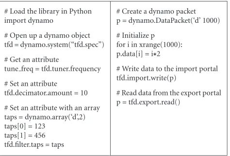
# Load the library in Python import dynamo
# Open up a dynamo object tfd=dynamo.system(“tfd.spec”) # Get an attribute
tune freq=tfd.tuner.frequency # Set an attribute
tfd.decimator.amount=10 # Set an attribute with an array taps=dynamo.array(‘d’,2) taps[0]=123
taps[1]=456 tfd.filter.taps=taps
# Create a dynamo packet p=dynamo.DataPacket(‘d’ 1000) # Initialize p
for i in xrange(1000): p.data[i]=i∗2
# Write data to the import portal tfd.import.write(p)
# Read data from the export portal p=tfd.export.read()
Figure12: Python DynamO example.
multithreaded environment as the application does not have to be concerned with the possibility of blocking on portal reads and writes. We have already implemented a DynamO front-end for C++, Python, and Rincon Research’s Midas 2k DSP environment.
The DynamO front-end is responsible for taking the Dy-namO object returned by the system method and trans-forming it into an object that the software environment can understand and access. For instance, using a Python front-end, the DynamO object is recreated in Python objects, with its methods mapped to the supplied DynamO object meth-ods.Figure 12demonstrates how a Python application script would interact with the DynamO API and the DynamO ob-ject in the TFD design example. Note that there is absolutely no evidence of implementation-specific details such as regis-ter addresses or communication protocols.
7. EXPERIMENTAL RESULTS
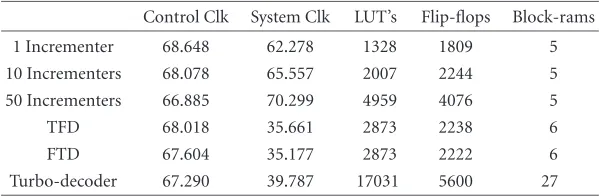
We have developed the Logic Foundry including all of the major building blocks described—VHDL implementations for MEADE, EP3, attribute interfaces, component abstrac-tions and interface portals, the get/set and data write/read portions of the DynamO API, DynamO back-ends for the Annapolis MicroSystems Starfire board, and DynamO front-ends for C++, Python, and Midas 2k. To test the effectiveness of the Logic Foundry, three systems have been developed, a series incrementer, the TFD, and a turbo decoder.
7.1. Incrementer design
The incrementer component consists of a streaming input portal, a streaming output portal, and an amountattribute that is added to the input before being passed to the output. We experimented with theincrementercomponent using an Annapolis MicroSystems Starfire board. This platform con-sists of four memory ports attached to an FPGA. Annapolis MicroSystems provides a shell for the FPGA, DMA bridges to transfer data from the PCI bus to the memory, and software driver calls to perform the DMA’s. To create the streaming
input and output portals, we modified the DMA bridges to add control for streaming data into and out of memory. Ad-ditionally, a DynamO library was created that provided por-tal write and read methods using the Annapolis DMA Driver calls wrapped with the extra control to manage the modifi-cations to the DMA bridges.
To control the Starfire card, Annapolis MicroSystems supplies driver calls to do addressable I/O via the PCI bus. However, the control is tightly timed and the Annapolis Mi-croSystems architecture implementing our portal function-ality requires seven control elements at the top level. When the number of elements attached to the control bus begins to exceed 10 or so elements, achieving the required timing of 66 MHz on a Xilinx XCV1000-4 can be difficult. For the Logic Foundry, we have built an attribute interface for all component control in the Starfire system and created Dy-namO interfaces to set/get attributes via this interface. The Starfire control bus is thus required to connect only to the DMA bridges, the attribute interface, and any top level con-trol registers required for operation. These connections re-main constant with the addition of new components.
To test the scalability of the Logic Foundry architecture, we createdincrementerdesigns consisting of 1, 10, and 50 in-crementercomponents connected together in series. In each case, system timing remained the same as the synthesis and layout tools were able to achieve the required 66-MHz con-trol timing for the Starfire concon-trol bus, while the attribute interface is scaled using the multicycle attribute bus (see
Table 1). It was initially our intention to do a design con-sisting of 100 serialincrementers, however, we reached a limit for the XCV1000 parts that only allows a tristate net to drive 98 locations. This limits an XCV1000 part to 98 components which is acceptable for our typical designs.
To create the different designs, we used a simple Perl script to generate the design specification files that instantiate and connect the components. All of the simulation, synthe-sis, and place and route steps were performed using simple MEADE commands.
7.2. TFD design
Table1: Summary of designs.
Control Clk System Clk LUT’s Flip-flops Block-rams
1 Incrementer 68.648 62.278 1328 1809 5
10 Incrementers 68.078 65.557 2007 2244 5
50 Incrementers 66.885 70.299 4959 4076 5
TFD 68.018 35.661 2873 2238 6
FTD 67.604 35.177 2873 2222 6
Turbo-decoder 67.290 39.787 17031 5600 27
included via the preprocesser. The processed VHDL files con-tain approximately 240 lines of VHDL code. The number of automated lines of code will vary depending on the number of attributes in the component. This same process was per-formed to create thefiltercomponent (using an FIR VHDL file created by the Xilinx Coregen tool). Thedecimator com-ponent was created with a few simple additions to the default MEADE template.
When all three components were completed, a design specification file was created (seeFigure 8) as well as an im-plementation specification file (seeFigure 9). These files were used by MEADE to create a complete implementation for the FPGA and system controlling software via the DynamO in-terfaces.
In order to test the ease of component reuse in the Logic Foundry, we opted to create an FTD system out of the TFD system components. To accomplish this task, the design spec-ification file was altered to change the connection order of the three components. MEADE was used to recreate the de-sign using the same implementation specification file. Dy-namO front-end objects were automatically changed due to the change in the design specification file. In both cases, con-trol timing was achieved and system timing was limited by the speed of the tuner component (seeTable 1).
7.3. The turbo decoder design
Our final design was to take a large design (several thou-sand lines of VHDL code) written outside of MEADE, but with a view to fitting into the Logic Foundry attribute/portal design structure. When the design was completed, it was wrapped with a MEADE component in the same manner as thetunerdescribed above. The turbo decoder design cre-ated unique challenges—firstly, the streaming portal design would not work as the turbo decoder worked on blocks of data and had to individually address these blocks of data. For this reason we created the block portal interface described in
Section 5.1.3.
The turbo decoder design required seven attributes and these were easily included via the attribute interface model. Implementing the block portals was more difficult as the completed turbo decoder design required eight unique block portals, five of which requiring simultaneous access. As the Starfire board had but four memories, this was a problem. However, as some of the portals did not require independent addressing, we were able to merge them into a single memory
and achieve an implementation that required four indepen-dently addressable memories. To accomplish this, we hand edited the implementation VHDL file and did not autogen-erate it from the implementation specification file.
This example showed that we could take a design and use some of the Logic Foundry without requiring tight tion into the whole of the Logic Foundry. Software integra-tion was done automatically, and the component architecture of the Logic Foundry was used, but the top level FPGA im-plementation specification and turbo decoder design and test were performed outside of the Foundry.
7.4. Summary of designs
Table 1shows results for each of the test designs implemented for the XCV1000-4 FPGA on the Annapolis MicroSystems Starfire board. Because control on this system is achieved via a 66-MHz PCI bus, the control clocks were all constrained to achieve this timing. In the case of the incrementer de-signs, the system clock performance was limited by the por-tal implementations. The other designs (TFD,FTD, turbode-coder) were limited by issues internal to their design com-ponents. Further development will be done to optimize the portal implementations for this architecture. The differences within design groups (incrementers and downconverters) are attributable to variances in the Xilinx software. The pseudo-random nature of the algorithms often results in variances. By doing a more extensive place-and-route operation, we would likely see these numbers converge.
8. CONCLUSION
be ported from platform to platform. Inserting a platform into a different software environment can also be done with relative ease.
While the entire Logic Foundry fits together as a whole, it is important to recognize that each piece can be used independently. One design house may simply want to use MEADE and EP3 as automation tools for FPGA construc-tion, where another design house may want to use the Dy-namO aspects without requiring any of the FPGA construc-tion mechanisms.
Our future work will focus on the complete implemen-tation of the data-synchronous control packets, component event control, and the control write/read portions of the Dy-namO API. We will also be integrating the Chameleon board from Catalina Research Incorporated as a demonstration of platform migration. Additionally, we plan on implementing a DynamO front-end for Matlab as well as a DynamO back-end for SystemC to allow algorithm emulation in software. We have implemented the Logic Foundry at Rincon Research and the tool is being used extensively in the development of high performance FPGA implementations of DSP applica-tions, including turbo coding, digital downconversion, and despreading applications.
ACKNOWLEDGMENT
S.S. Bhattacharyya was supported in part by the National Sci-ence Foundation, Grant no. 9734275, and the Advanced Sen-sors Collaborative Technology Alliance.
REFERENCES
[1] R. T. Olay III, “Xilinx XtremeDSP initiative meets the demand for extreme performance and flexibility,” Xcell Journal, , no. 40, pp. 30–33, Summer 2001.
[2] U. Meyer-Baese, Digital Signal Processing with Field Pro-grammable Gate Arrays, Springer-Verlag, Berlin, Germany, 2001.
[3] P. Banerjee, N. Shenoy, A. Choudhary, et al., “MATCH: A MATLAB compiler for configurable computing systems,” Tech. Rep. CPDCTR-9908-013, Center for Parallel and Dis-tributed Computing, Northwestern University, Evanston, Ill, USA, August 1999.
[4] OXFORD Hardware Compilation Group, “The Handel lan-guage,” Tech. Rep., Oxford University, Oxford, UK, 1997. [5] J. Gerlach and W. Rosenstiel, “System level design using
the systemC modeling platform,” http://www.systemc.org/ projects/sitedocs/.
[6] P. Bellows and B. Hutchings, “JHDL—An HDL for recon-figurable systems,” inProc. IEEE Symposium on FPGAs for Custom Computing Machines, pp. 175–184, Napa, Calif, USA, April 1998.
[7] H. Chang, L. Cooke, M. Hunt, G. Martin, A. McNelly, and L. Todd, Surviving the SOC Revolution: A Guide to Platform-Based Design, Kluwer Academic Publishers, Boston, Mass, USA, 1999.
[8] Xilinx System Generator v2.1 for Simulink Reference Guide, Xilinx, San Jose, Calif, USA, 2000.
[9] J. Donaldson, “From algorithm to hardware—The great tools disconnect,”COTS Journal, vol. 3, no. 10, pp. 48–54, 2001.
[10] J. T. Buck, S. Ha, E. A. Lee, and D. G. Messerschmitt, “Ptolemy: A framework for simulating and prototyping het-erogeneous systems,” International Journal of Computer Sim-ulation, vol. 4, pp. 155–182, April 1994.
[11] F. Balarin, P. Giusto, A. Jurecska, et al., Hardware-Software Co-Design of Embedded Systems: The Polis Approach, Kluwer Academic Publishers, Boston, Mass, USA, 1997.
[12] E. Pauer, C. Myers, P. D. Fiore, et al., “Algorithm analysis and mapping environment for adaptive computing system,” inProc. 2nd Annual Workshop on High Performance Embed-ded Computing, pp. 264–265, Boston, Mass, USA, September 1998.
[13] S. Natarajan, B. Levine, C. Tan, D. Newport, and D. Bouldin, “Automatic mapping of Khoros-based applications to adap-tive computing systems,” inProc. 1999 Military and Aerospace Applications of Programmable Devices and Technologies Inter-national Conference (MAPLD), pp. 101–107, Laurel, Md, USA, September 1999.
[14] D. Argiro, K. Farrar, and S. Kubica, “Cantata: The visual pro-gramming environment for the Khoros system,” inProc. In-ternational Conference Visualization, Imaging and Image Pro-cessing (VIIP 2001), Marbella, Spain, September 2001. [15] R. Rajsuman, System-on-a-Chip: Design and Test, Artech
House Publishers, Norwood, Minn, USA, 2000.
[16] M. Keating and P. Bricaud, Reuse Methodology Manual for System-On-A-Chip Designs, Kluwer Academic Publishers, Boston, Mass, USA, 2nd edition, 1999.
[17] Rincon Research Corporation, Tucson, Ariz, USA, Introduc-tion to Midas 2k, January 2000.
[18] R. Andraka, “High performance digital down-converters for FPGAs,”Xcell Journal, , no. 38, pp. 48–51, Winter 2000. [19] Annapolis Micro Systems Incorporated, Annapolis, Md, USA,
WILDSTAR Reference Manual, rev 3.1, 2000.
[20] C. Matsumoto, “EE Times.com,” inCoverage of the FPGA2000 Panel discussion evaluating the ability of CAE tools for FPGAs, Monterey, Calif, USA, February 2000.
[21] G. Spivey and K. Nakajima, “The philosophy of MEADE: A Modular, Extensible, Adaptable Design Environment,” in Proc. International HDL Conference and Exhibition (HDL-CON), pp. 159–165, San Jose, Calif, USA, March 1999. [22] G. Spivey, “MEADE, A Modular Extensible Adaptable Design
Environment for ASIC and FPGA development,” inPerl Con-ference 3.0, San Jose, Calif, USA, July 1999.
[23] D. Conway,Object Oriented Perl, Manning, Greenwich, Conn, USA, 1999.
[24] B. Cohen, Component Design by Example, VhdlCohen Pub-lishing, Palos Verdes Peninsula, Calif, USA, 2001.
[25] G. Spivey, “EP3: An extensible Perl PreProcessor,” inProc. In-ternational Verilog HDL Conference and VHDL InIn-ternational Users Forum, pp. 106–113, Santa Clara, Calif, USA, March 1998.
[26] S. Sriram and S. S. Bhattacharyya,Embedded Multiprocessors: Scheduling and Synchronization, Marcel Dekker, New York, NY, USA, 2000.
[27] M. Newman and S. Newman, “New solutions for reconfig-urable electronics: Developing prototypes and reconfigreconfig-urable equipment with Celoxica and Wind River,” Celoxica White Paper.
Gary Spivey received his B.S.E.E. degree from the University of Arizona in 1988 and his M.S. and Ph.D. degrees from the University of Maryland at College Park, in 1997 and 2001, respectively. From 1988 un-til 1999, he was a system and ASIC Designer with the National Security Agency and is currently a Senior Member of the techni-cal staff of Rincon Research Corporation. His current research interests include rapid
FPGA prototyping and hardware mappings for DSP algorithms.
Shuvra S. Bhattacharyya is an Associate Professor in the Department of Electrical and Computer Engineering, and the Insti-tute for Advanced Computer Studies (UMI-ACS) at the University of Maryland, College Park. He is the coauthor of two books and the author or coauthor of more than 50 ref-ereed technical articles, Dr. Bhattacharyya is a recipient of the NSF Career Award. His research interests include signal processing,
embedded software, and hardware/software codesign. He received the B.S. degree from the University of Wisconsin at Madison, and the Ph.D. degree from the University of California at Berkeley. Dr. Bhattacharyya has held industrial positions as a Researcher at the Hitachi America Semiconductor Research Laboratory, and as a Compiler Developer at Kuck & Associates.