AVSynDEx: A Rapid Prototyping Process Dedicated
to the Implementation of Digital Image Processing
Applications on Multi-DSP and FPGA Architectures
Virginie Fresse
CNRS UMR IETR (Institut en Electronique et T´el´ecommunications de Rennes), INSA Rennes, 20 avenue des Buttes de Co¨esmes, CS 14315, 35043 Rennes Cedex, France
Email: [email protected]
Olivier D ´eforges
CNRS UMR IETR (Institut en Electronique et T´el´ecommunications de Rennes), INSA Rennes, 20 avenue des Buttes de Co¨esmes, CS 14315, 35043 Rennes Cedex, France
Email: [email protected]
Jean-Franc¸ois Nezan
CNRS UMR IETR (Institut en Electronique et T´el´ecommunications de Rennes), INSA Rennes, 20 avenue des Buttes de Co¨esmes, CS 14315, 35043 Rennes Cedex, France
Email: [email protected]
Received 31 August 2001 and in revised form 12 May 2002
We present AVSynDEx (concatenation of AVS + SynDEx), a rapid prototyping process aiming to the implementation of digital signal processing applications on mixed architectures (multi-DSP + FPGA). This process is based on the use of widely available and efficient CAD tools established along the design process so that most of the implementation tasks become automatic. These tools and architectures are judiciously selected and integrated during the implementation process to help a signal processing specialist without relevant hardware experience. We have automated the translation between the different levels of the process to increase and secure it. One main advantage is that only a signal processing designer is needed, all the other specialized manual tasks being transparent in this prototyping methodology, hereby reducing the implementation time.
Keywords and phrases:rapid prototyping process, multi-DSP-FPGA architecture, CAD environment, image processing applica-tions.
1. INTRODUCTION
The prolific evolution of telecommunication, wireless and multimedia technologies has sustained the requirement for the development of increasingly complex integrated sys-tems. Indeed, digital signal processing applications includ-ing image processinclud-ing have become more and more com-plex, thereby demanding much greater computational per-formances. This aspect is especially crucial for certain real-time applications. To validate a new technique only func-tionality is not sufficient, the algorithm has to be executed in a limited time. Until then the first approach to meet this aspect was to optimize the algorithm, a digital signal or im-age designer could do this task. Nevertheless, this solution was quickly inadequate, and parallel to the algorithm devel-opment, the implementation aspect must be taken into ac-count. The use of parallel architectures distributes and then accelerates the execution time of the application.
Currently, one of the best solutions is mixed platforms in-tegrating a combination of standard programmable proces-sors and a hardware part containing components like FPGA, ASIC, or ASIP. It has been demonstrated in [1, 2, 3] that such architectures are well suited for complex digital image pro-cessing applications: the distribution between both parts is generally done by implementing the elementary and regular operations in the hardware part, the other processing steps being processed by the software part. These platforms can deliver higher performances but this heterogeneous aspect involves software and hardware engineering skills.
lose their initial correlation. Moreover, it is difficult to man-age all the tasks, especially the shared resources and the asso-ciated synchronizations [4, 5].
The negative side of such implementations on com-plex and parallel architecture is the long development time emerging from the number of specialized people involved in the process. The signal processing designer does not have any more the sufficient skills to supervise the com-plete development, the error detection at each level becom-ing more difficult. The intervention of several engineers in-volves a task partitioning between the different parts at the beginning of the process, and a partitioning modification is very difficult as another complete implementation is often required.
Most of computer-aided design (CAD) environments dedicated to the implementation on parallel and mixed ar-chitectures are called codesign tools [6, 7, 8] and they inte-grate a manual and arbitrary partitioning based on the de-signer experience. The present codesign tools can address the problem of implementation either on multistandard pro-cessors, or one processor and a dedicated hardware, but not both of them, which is the topic of this paper.
An example of codesign tool is POLIS (which is pre-sented in [9]). This tool is dedicated to embedded systems, which support the control flow description. The representa-tion is CSFM, codesign finite state machine and the advan-tage of this one is its independence with the target architec-ture. There is also Chinook, which is dedicated to reactive real-time systems (as explained in [10]).
The objective of this work is to propose a full rapid proto-typing process (AVSynDEx) by means of existing academic, commercial CAD tools and platforms. A translator between the CAD environments allows going automatically through the process.
The prototyping methodology enables a digital signal or image-processing designer to create the application with a usual development environment (advanced visual system) and then to supervise the implementation on a mixed ar-chitecture without any other necessary skills. AVSynDEx is open-ended and can realize the partitioning between soft-ware/hardware target at the highest level of the application description.
The approach consists of starting with a customary en-vironment used by the digital signal processing developer. Then the integration of a distributed executive generator SynDEx (synchronised distributed executive) leads to an op-timized implementation on a parallel and mixed platform. The target architecture combines a multi-DSP (digital signal processor) part with an FPGA (field programmable gate ar-ray) platform. A main characteristic is the presence of check-ing points at each level of the implementation process ac-celerating the development time: the designer can check and correct his design immediately without waiting for the im-plementation. This aspect gives the designer the possibility to easily and quickly modify the algorithm or to change its implementation.
This prototyping process leads to a low production cost: SynDEx is a free academic CAD tool and the multi-DSP and
FPGA board is profitable compared to the development, time and cost (including raw material, specialized engineers and specific equipment) for a new platform. Moreover, this pro-totyping process can integrate the new versions of the CAD tools and also can use their new performances.
The remainder of this paper is organized into 5 sections. Section 2 gives an overview of the prototyping process by briefly introducing the CAD environments as well as the tar-get architecture. Section 3 details all these elements. The pro-totyping methodology is fully described by explaining the compatibility requirements between the levels of the process, and introducing the automatic translator. By way of process illustration, the implementation of an image compression al-gorithm LAR is given in Section 5. Section 6 concludes the paper.
2. OVERVIEW OF THE PROTOTYPING PROCESS
The prototyping process (Figure 1) aims to a quasi-auto-matic implementation of digital signal or image applica-tions on parallel and mixed platform. The target architec-ture can be homogeneous (multiprocessor part) or hetero-geneous (multi-DSP + FPGA). A real-time distributed and optimized executive is generated according to the target plat-form.
The digital image designer creates the data flow graph by means of the graphical development tool AVS. This CAD software enables the user to achieve a functional validation of the application. Then, an automatic translator converts this information into a new data flow graph directly compatible with the second CAD tool, SynDEx. This last tool schedules and distributes the data flow graph according to the paral-lel architecture and generates an optimized and distributed executive. This executive is loaded onto the platform by us-ing GODSP, a loader and debugger tool. These tools are quite simple and the links between them are automatic, accelerat-ing the prototypaccelerat-ing process.
The target applications are complex digital image pro-cessing algorithms, whose functions possess different gran-ularity levels. The partitioning consists generally of imple-menting the regular and elementary operations on the FPGA part and the higher-level operations on the multi-DSP part. The prototyping process has the advantage to take this parti-tioning aspect into account and to ensure an adjustable and quickly modifiable decision. The image-processing designer is not restricted to one implementation and the partitioning modifications are quickly realized.
Three elements are necessary for this prototyping pro-cess: the CAD tools, the target architecture, and the links for an automatic process.
3. PRESENTATION OF THE INTEGRATED CAD TOOLS AND THE MIXED PLATFORM
Data
flow graph AVS Automatictranslator SynDEx Sequential
executive Workstation
PC
Sequential executive distributed executive
GODSP Multi-DSP
+ FPGA board
Figure1: The prototyping process. It consists of one graphical image development tool AVS, SynDEx, which is dedicated to the generation of parallel and optimized executive and a loader-debugger GODSP. The links between these CAD environments are automatic. The data flow graph is implemented on a multi-DSP + FPGA board.
a distributed and optimized executive. A third tool, a trans-lator between AVS and SynDEx realized the automatic link.
The target architecture is a mixed platform with a multi-DSP part and an FPGA one.
3.1. AVS: advanced visual system
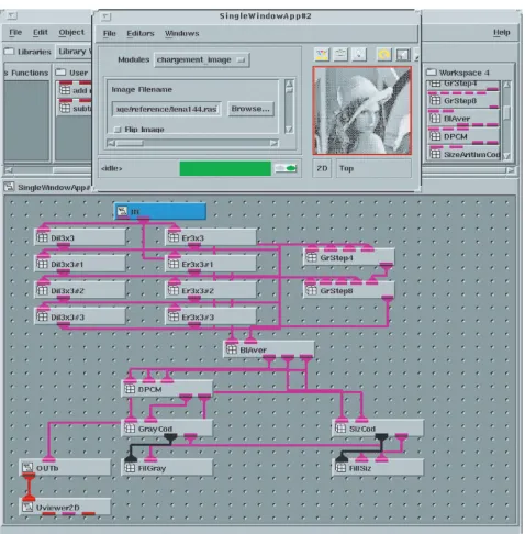
AVS (advanced visual system) is a high-level environment for the development and the functional validation of graphical applications [11]. It provides powerful visualization meth-ods, such as color, shape, and size for accurate informa-tion about data, as shown in Figure 2. The AVS environment (Figure 3) contains several module libraries located on top and a workspace dedicated to the application developments. These algorithms are constructed by inserting existing mod-ules or user modmod-ules into the workspace. A module is linked to its input and output images and their corresponding types. Each module calls a C, C++, or Fortran function and the associated library files. During a modification of an exist-ing function, the module is immediately updated and the algorithm as well. All these modules are connected by in-put and outin-put ports to constitute the global application in the form of a static data flow graph. In the following, we consider that traded data are mainly images represented as one-dimensional array. AVS includes a subset of visualiza-tion modules for data visualizavisualiza-tion, image processing, and user-interface design.
A main advantage is the automatic visualization of inter-mediate and resulting images at the input and output of each module. This characteristic enables the image-processing de-signer to check and validate the functionality of the applica-tion before the implementaapplica-tion step.
3.2. SynDEx
SynDEx is an academic system-level CAD tool [13, 14]. This free tool is an academic environment designed and devel-oped at INRIA, Rocquencourt France and several national laboratories take part in this project as we does. SynDEx is an efficient environment, which uses the AAA methodology to generate a distributed and optimized executive dedicated to parallel architectures.
AAA stands for algorithm architecture “ad´equation,” ad´equation is a French word meaning an efficient match-ing (note that it is different from the English wordadequacy,
Figure2: Examples of AVS applications. Above, theTracking Money Launderersand below,Bright Forecastat theNational Weather Ser-vice[12]. These examples use the color, size, and shape for data vi-sualization.
Figure3: The AVS environment. Above, the libraries containing the available modules. A rectangle is a defined module. The designer can create and insert the modules into those libraries. The red and pink marks represent the input and output; the color indicates the type of the ports. Below, the workspace for the algorithm creation. The visualization of an image is done by inserting theUviewer2Dmodule and connecting to the target module (here, it is the output moduleOUT).
supported processor. These primitives support boot load-ing, memory allocation, intercomponent communications, sequentialisation of user supplied computation functions, of intercomponent communications and intersequences syn-chronization.
SynDEx ensures the following tasks [16].
(i) Specification of an application algorithm as a con-ditioned data flow graph (or interface with the compiler of one of the Synchronous languages ESTEREL, LUSTRE, SIG-NAL through the common format DC). The algorithm is de-scribed as a software graph.
(ii) Specification of the multicomponent architecture as a hardware graph.
(iii) Heuristic for distributing and scheduling the algo-rithm on the architecture with response time optimization.
(iv) Visualization of predicted real-time performances for the multicomponent sizing.
(v) Generation of deadlock-free executives for real-time execution on the multicomponent with optional real-time performance measurement. These executives are built from a processor-dependent executive kernel [17]. SynDEx comes currently with executives kernels for digital signal proces-sor and microcontroler: SHARC-ADSP21060, TMS320C4x, Transputer-T80X, i80386, i8051, i80C96, MC68332, and for workstations: UNIX/C/TCP/IP (SUN, DEC, SGI, HP, PC Linux). Executive kernels for other processors can be eas-ily ported from the existing ones. The shared resources and the synchronizations are taken into account. SynDEx trans-fers images by using static memory whose allocation is
op-timized. The current development work with SynDEx is to refine the communication media and to target the use of this tool to mixed architectures (including FPGA and other ASIC). So this evolution will be still coherent for future com-plex products.
The SynDEx environment is shown in Figure 4. The edi-tion view contains two graphs: the hardware architecture above and the software graph below. The hardware graph represents the target architecture with the hardware compo-nents and the physical links whereas the software graph is the data flow graph of the application: the vertex is a “task” (compiled sequence of instructions), and each edge is data-dependent between the output of an operation and the input of another task. The vertex is defined by means of informa-tion such as the input and output images, the size and type of these images, the name of the corresponding C-function and the time execution. If the execution time is not known, a first random value must be affected for every function. Any random value can be used but a by default value is chosen to obtain an automatic translation and generate the executive by means of SynDEx. Then, SynDEx generates a first sequen-tial executive on a monoprocessor implementation in order to determine the real task time.
The granularity level of the graph has an impact on the final implementation: many vertices lead to more parallelism but also increase the data communication cost.
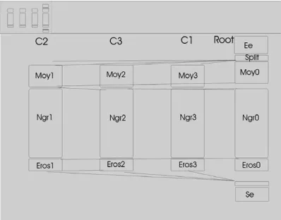
Figure4: SynDEx CAD software: the workspace. Above, a target architecture with 4 DSP, C4, C3, C2, and root. Root is the DSP, which is dedicated to the video (grab and display image): the input and output functions are processed by this processor. The physical connections are represented. Below, the software graph (algorithm) contains processing tasks (edges) and the data dependencies (ver-tices). Ee and Se are respectively the input and output images.
Figure5: The SynDEx timing diagram. Each column represents the task allocation for one DSP (Moy1, Ngr1, and Eros1 are treated by the DSP C2 and the video modules Ee and Se are effectively imple-mented on the video DSP root). The size of each rectangle is the execution time for every task and the lines between the columns indicate the communication transfers. This diagram shows the par-allelism of the algorithm and the timing estimation.
communication medium. The timing diagram describes the distribution (spatial allocation) and the scheduling (tempo-ral allocation) of tasks on processors, and of interproces-sor data transfers on communication media. Time is flowing from top at bottom and the height of each box is propor-tional to the execution duration of the corresponding opera-tion.
SynDEx is an efficient tool for the implementation on parallel architectures but is not an application development tool environment as it is not able to simulate the software graph. Without any front-end tool, the signal processing de-signer has to create a sequential C-application by means of
current C-development tools. Once the functional validation is done, it has to be split into several functions for the Syn-DEx data flow graph; each function represents an edge in the SynDEx data flow graph. The resulting data flow graph can be checked only after the implementation on the target plat-form. The manually transformation of the SynDEx data flow graph can generate some mistakes. Moreover, optimization is quite long and not automatic: the image processing designer has to work with the initial algorithm, the SynDEx tool and the transformations between these two data flow graphs.
3.3. The multi-DSP-FPGA platform
The development of this own parallel architecture is a very complex task while suppliers offer powerful solutions. It is the reason why we have opted for a commercial product. The choice of the target architecture has been directed by different motivations. Firstly, the platform had to be generic enough in order to integrate most of the possible image applications. Secondly, it had to be modular to be able to evolve with time. Thirdly, the architecture programming had to be at sufficient level in order to be interfaced with SynDEx. Fourthly, the cost had to be reasonable to represent a realistic solution for pro-cessing speedup.
The experimental target architecture is a multi-DSP and FPGA platform based on a Sundance PCI motherboard, Sun-dance Multiprocessor technology Ltd., Chiltern House, Wer-side, Chesham, UK, whose characteristics enable the user to obtain a coherent and flexible architecture.
Two Texas Instrument Modules (TIM) constitute the multi-DSP part [18, 19]. The first one integrates two TMS320C44 processors to carry out the processing. The sec-ond module is a frame-grabber containing one TMS320C40 DSP. When it is not used for a video processing, this DSP can run image as well.
An additional FPGA part (Figure 6) is designed as a reconfigurable coprocessor for TMS320C4x based-systems and is associated to this multi-DSP platform. This is a MIROTECH X-C436 board [19] integrating a XC4036 FPGA, fully compatible with the TIM specifications: this module can be directly integrated onto the motherboard.
This FPGA is used as two virtual processing elements called VPE. Each VPE is considered as one FPGA XC4013, the rest of the full FPGA being used for the communication port management: all external transfers between the mod-ules and the multi-DSP architecture are resynchronized by a communication port manager (CPM). The designers of this board propose this solution, which will be used for the pro-totyping process and they give the existing cores (a core is a processing task for one VPE) for this configuration. Never-theless, it can be extended to different size of VPE and dif-ferent number of VPE on the sole condition that the image-processing designer or a hardware engineer creates the spe-cific cores.
CSU
CPM
Comms port JTAG ILINK
VPE1
VPE2
SRAM
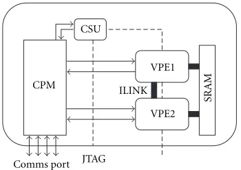
Figure6: The X-CIM architecture. The FPGA includes 2 VPE dedi-cated to achieve the image processing. ILINK is a direct link between both. The CPM is responsible for the communications between DSP and FPGA. A supervisor, Configuration and Shutdown Unit, con-trols the clock and the reset.
P2 P1 Root
VPE1 VPE2
FPGA
Figure7: The proposed multi-DSP FPGA topology. The multi-DSP part contains 3 DSP called root, P1, and P2, root being the video processor. The black squares are the physical links between DSP. The FPGA part is the coprocessor for the root DSP. Each VPE have one input and one output, which are connected to the root DSP. The FPGA part (grayed) is fully transparent to the user and the functions are managed by the root processor.
inside the DSP code. A configuration step is necessary be-fore the processing step. The configuration step includes the initialization of the module (link specifications between the VPE and DSP, license affectation), the parameters for each core (data size, image size, . . . ), core assignations for each VPE and the module configuration (implementation of all previous configurations on the board).
Afterwards, the processing can be achieved in 3 possible ways.
(i)Transparent communication mode. The first solution consists of using one instruction corresponding to the target processing. The input and output images are the only nec-essary parameters: this only instruction ensures to send the input images to FPGA and then to receive the output images at the end of the execution. This unique instruction is easy to use but prevents the processor running a parallel function.
(ii) Low-level communication mode. In a second ap-proach, the user gives the input and output image by using some pointers and sends the images pixel per pixel, which are immediately processed and then sent back. With this method, a function is time-consuming and the processor cannot run another function in the same time.
(iii)DMA communication mode. The last way consists of sending the input image via the DMA. Specific instructions enable the designer to associate the image, to read and write in the DMA, and to wait for the end of the processing. The advantage is that the processor can execute another process at the same time.
For all these processing possibilities, specific libraries contain cores and specific instructions for the FPGA config-uration and use. The library declaration is inserted in these functions.
The configuration and processing tasks can be separated and included in different functions. The configuration time of the dedicated module is long (about 2.6 seconds), limiting to a static use of the coprocessor to two type of operation.
4. PROTOTYPING METHODOLOGY FOR MIXED
AND PARALLEL ARCHITECTURES
AVSynDEx is a prototyping process aiming to go automati-cally from the functional AVS description to the distributed execution over the multi-DSP or mixed architecture (see Figure 1). It implies first to guaranty a full compatibility be-tween the elements throw the process, and then to generate automatic links. The general requirements for a multi-DSP implementation are listed first, before the specific ones linked to the dedicated target.
4.1. Compatibility for multi-DSP architectures 4.1.1 SynDEx-multi-DSP platform
SynDEx can handle the multi-DSP architecture once the syn-chronization primitives, memory management, and com-munication schemes have been realized for the type of pro-cessors involved. Architecture configurations such as frame grabber initialization are gathered in an INIT file executed once at the beginning of the application running.
4.1.2 AVS-SynDEx
SynDEx and AVS present a similar semantic in terms of ap-plication description with the use of static data flow graph. Nevertheless, some particularities have to be dealt with.
Restrictions in SynDEx description
Only a few data types are defined in SynDEx (Boolean, inte-ger, real, . . . ), and the dimension of the arrays must be fixed. The same rules have to be applied for the AVS graphs.
C-functions associated to processing vertices
For both graphs, each vertex can be associated to a C-function. A skeleton of the function is generally created by AVS when editing a new module, containing specific AVS in-structions to interface the user code to the global applica-tion. To be compiled in the SynDEx environments, all these instructions have to be removed.
Specific vertices
h-files
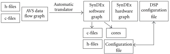
Figure8: Presentation of the automatic translator.
read and write image files, whereas it is linked to video cap-ture and display for SynDEx.
Besides the processing vertices, SynDEx defines also three specific ones:
(i) Memory: a storage element acting as a FIFO whose deep is variable.
(ii) When: allows to build a conditional graph (the follow-ing of the graph is executed if an input condition is asserted).
(iii) Default: selects between two inputs the one to be trans-mitted depending on an input condition.
The corresponding AVS primitives have been designed in V (the low-level language of AVS) to keep the whole SynDEx potential of graphs management.
4.2. Compatibility specific to FPGA module
4.2.1 SynDEx-Mixed platform
As the FPGA module management is carried out by a host DSP, the adopted solution consists of representing the use of a VPE in the data flow graph by a dedicated vertex linked to the host. The associated function contains only the reference to the core according to the transparent com-munication mode. The essential advantage is that the data flow graph remains unchanged compared to the multi-DSP case: whatever the target architecture is (software or hard-ware), a task is specified by its inputs, outputs, and executive time.
FPGA module configuration is also stored in the global INIT file.
4.2.2 AVS-SynDEx
In order to get equivalent functional graph, a functional equivalent C-function has to be developed for each available core, gathered in a library. It is an easy task as the low-level treatments corresponds generally to simple algorithms. For a multi-DSP architecture only, the function can be directly reused and implemented into a DSP. When using the FPGA module, it has to be replaced by the call to the core.
4.3. The automatic translator
The fulfillment of the compatibility between the prototyp-ing process stages allows to go from the functional descrip-tion to the parallel implementadescrip-tion. By designing a translator
between AVS and SynDEx, the process is performed auto-matically.
The automatic translator is designed with the Lex and Yacc tools. The first one filters the necessary parts in a se-quence whereas the second one transforms an input chain into another one.
The translator realizes the following tasks, as shown in Figure 8:
(i) Transforms the AVS data flow graph syntax into a Syn-DEx one.
(ii) Looks for user c-files and h-files associated to each module and “cleans” them of specific AVS instruc-tions.
(iii) Transforms Memory, When, and Default primitives into SynDEx ones.
(iv) Generates the constraints (e.g., IN and OUT linked to the host DSP).
(v) Adds automatically the target architecture (hardware graph).
(vi) Generates the INIT file for the multi-DSP configura-tion.
Moreover, the translator is a key element in the codesign process. A flag is associated to each core equivalent AVS ule that indicates if the target is a DSP or the hardware mod-ule. In the first case, the c-file and the h-files are fetched and reused for the generation of the executive. In the second case, these files are replaced with the corresponding core and the FPGA configuration is added to the INIT file. Thus, the al-location/partitioning tasks are easily done in the functional environment.
AVS
Specifications
Data flow graph
Data flow graph
SynDEx
Sequential executive
DSP implementations
Timing measurement User User
Allocation/Partitioning
Data flow graph
Data flow graph
Spatial and temporal scheduling
Distributed executive
FPGA+multi-DSP implementation
C-functions
cores
GODSP
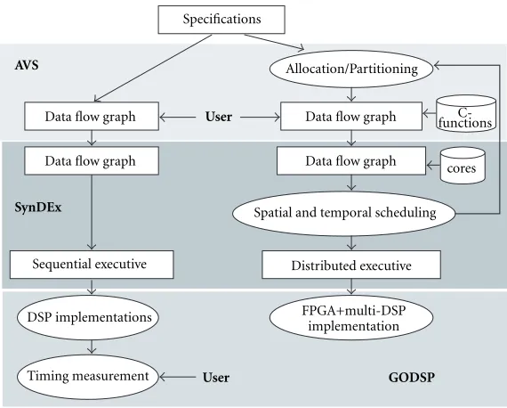
Figure9: The AVSynDEx prototyping methodology for mixed and parallel architecture. The starting point is the specification for a data flow graph creation. Two runs of the implementation process are necessary: the first one is the chronometrical report by means of a sequential executive (left part). It is necessary only for new C-functions and is removed in the other case. The second one is the implementation on the mixed platform. The links between the CAD tools are automatic and the designer supervises all the implementation steps.
4.4. Prototyping process
The implementation process is simple, requiring only a max-imum of two development presented in Figure 9. For new user C-modules, their executive time has first to be deter-mined to get eventually an optimized parallel implementa-tion. It is done by first considering a mono-DSP target, when the user constraints all the tasks of the software graph to be associated to the root processor. The executive generated by SynDEx is at this step only sequential. The loader GODSP en-sures the implementation of the application and the report of the chronological information. Then, the designer has only to copy out these times on the AVS modules. If the applica-tion is made of already valued C-modules, this first run of the process is of course useless.
Once the algorithm is functionally validated and the par-titioning is decided by the designer, the automatic transla-tor generates the new SynDEx description associating the C-functions and the cores. From now on, the hardware graph is the multi-DSP architecture. SynDEx schedules and dis-tributes the algorithm and gives the resulting timing dia-gram. The user can choose to modify the partitioning in AVS or run the application on the mixed platform.
The main advantage of this prototyping process is its sim-plicity, as most of the tasks realized by the users concern the application description with his conventional environment. The required knowledge of SynDEx and the loader are lim-ited to simple operations.
Other front-end development tools can be used in the process instead of AVS so far as they present a similar seman-tic for the application description. Ptolemy-related works can
be found in [20, 21]. AVSynDEx can be adapted to other ar-chitectures as well.
5. IMPLEMENTATION OF AN IMAGE COMPRESSION
ALGORITHM
A new image compression algorithm has been developed in our laboratory: its implementation on a mixed architecture provides a validation of our fast prototyping methodology. This algorithm called LAR, locally adaptive resolution [20], is an efficient technique well suited for image transmission via Internet or for embedded systems. Basically, the LAR method was dedicated to gray levels still image compression, but extensions have been also proposed for colour images and videos [22].
5.1. Principle of the compression
The basic idea of the LAR method is that the local resotion (pixel size) can depend on the activity: when the lu-minance is locally uniform, the resolution can be low (large pixel size). When the activity is high, the resolution has to be finer (smaller pixel size).
A first coder is an original spatial technique and achieves high compression ratio. It can be used as a stand-alone tech-nique, or complemented with a second coder allowing to en-code the error image from the first en-coder topology descrip-tion. This second one is based on an optimal block-size DCT-transform. This study concerns only the first spatial coder. Figure 10a presents its global process.
rep-Source image
Figure10: (a) Global scheme of the spatial LAR coder. (b) Decom-position of the nonuniform function.
resenting local trees. Then, each one is split according to a quadtree scheme depending on the local activity (edge pres-ence). The finest resolution is typically 2×2 squares. The image can be reconstructed by associating to each square the corresponding average luminance in the source image.
The image contents information given through the square size is considered advantageous for the luminance quantization. Large squares require a fine quantization, as they are located in uniform area (strong sensitivity of human eye to brightness variations). Small ones support a coarse quantization as they are upon edges (low sensitivity). Size and luminance are both encoded by an adaptive arithmetic entropic encoder. The average cost is less than 4 bits per square.
5.2. Functional description of the application by means of AVS
In order to obtain the best implementation of the data flow graph on the mixed architecture, the image processing de-signer has to exhibit both elementary operations available in the core library and additional data parallelism allowed by some tasks. All the decisions and modifications are achieved only at the functional level (AVS data flow representation).
In the LAR method, block stationary property is evalu-ated by a morphological gradient followed by a threshold. A morphological gradient is defined as the difference between the dilated value (maximal value in a predefined neighbour-hood) and the eroded value (minimal value in the same neighbourhood). A low resulting value indicates a flat region. A high ones show offan edge in the neighbourhood. By com-puting this stationary estimation using growing neighbour-hood surface (2×2, 4×4, 8×8, and 16×16), it is possi-ble to choose the maximal block size to represent the region while keeping the stationary property. The major drawback of this approach is that the morphological operators com-plexity is proportional to the neighbourhood size, and then an erosion/dilation upon a 16×16 block requires 256 op-erations per pixel. To reduce the complexity, one uses gen-erally the Minkowski addition by performing an operation upon a large neighbourhood as successive operations upon smaller neighbourhood [23]. As 3×3 erosion and dilation operators are available in the core library, the graph modifi-cations at this stage have consisted of decomposing the global morphological operations into iterative elementary ones (see Figure 10b).
Data parallelism has been also pointed out for a mul-tiprocessing purpose as most of the other functions are lo-calised into 16×16 blocks.
The algorithm development and optimizations are achieved using the AVS tool. The designer can develop the application and can easily refine the granularity of several functions. The data flow graph algorithm of the LAR appli-cation is developed and the resulting AVS data flow graph is shown in Figure 11. AVS enables the image processing de-signer to check the functionality of the new algorithm as shown in Figure 12.
5.3. Implementation on the multi-C4x-FPGA platform According to the presented prototyping process, the auto-matic translator generates the corresponding SynDEx data flow graph and the associated files. A first monoprocessor implementation is required for chronological measurements and the modules are specified to be software modules. Syn-DEx generates a sequential executive for the implementation on the root processor. The designer does the chronometrical reports (Table 1) and inserts these new times in the AVS data flow.
The time corresponding to a C4x-processor implementa-tion is 3.21 seconds and represents the reference for the par-allel one.
con-Figure11: Presentation of the LAR algorithm under the AVS en-vironment. On top, the new modules are inserted into libraries (right). Below, the data flow graph of the LAR application. The out-put image is visualized by means of the Uviewer2D module: it is the Lena image.
sists only of removing the constraint of tasks allocation to only one DSP in SynDEx.
The best distribution according SynDEx is using only 2 C4x-processors (root and P1). This timing diagram shows that the global time should be longer or not more efficient in case of a 3DSP implementation. The resulting time for this implementation is 1.74 seconds.
As the 3×3 erosion and dilation cores are available, the last solution consists in the use of the FPGA to perform these operations. A comparison with the software implementa-tion shows that the hardware one is approximately 100 times faster. Note that the architecture limits the number of cores in an application but theses cores can be used several times (several identical vertices in the graph). Changing the tar-get flag of the equivalent AVS modules and running again the translator leads to a new SynDEx input file. The Er3∗3 and Dil3∗3 C-functions are replaced by the call of the cor-responding cores. The SynDEx data flow graph remains un-changed except new constraints on the FPGA tasks allocated to the host (root) processor. Then, SynDEx can schedule and distribute the application according to the new software and material graphs. The timing diagram is almost the same than Figure 14 except erosion and dilation tasks, which are much smaller. The resulting executive time is 245 milliseconds.
5.4. Implementation on a multi-C6x platform: AVSynDEx version 2
The new Sundance multiprocessor architecture is now avail-able and an upgrade of AVSynDEx (version 2) to this new
ar-Table1: Modules execution time (image 120×120 pixel).
Functions Time (microsecond)
DSP C4X FPGA DSP C6X
IN 50 648
Er3∗3 371 400 (∗4) 4 176 (∗4) 18 551 (∗4) Dil3∗3 370 681 (∗4) 4 150 (∗4) 18 410 (∗4)
GrStep4 6 777 562
GrStep8 5 967 636
BlAver 7 558 11 124
DPCM 33 886 14 721
SiZcod 71 586 3 243
GrayCod 64 275 3 193
FilGray 2 816 232
FilSiz 2 859 243
OUT 12 141
(a) Original image (512∗512, 8 bits per pixel).
(b) Nonuniform grid.
(c) Reconstructed image. (d) Reconstructed image after postprocessing (0.18 bits per pixel, PSNR 28.5 dB).
Figure12: Visualization of images in the AVS environment. Image display is available via an Uviewer2D module.
Table2: Comparisons of different ameliorations given by the prototyping process. The proposed prototyping process improves the devel-opment time and is friendlier. The optimizations and functional validation ensure to improve the application description and to obtain a rapid implementation. The partitioning is easier as the SynDEx tool is not being friendly for such modifications.
Full development Translation AVS-SynDEx Functional validation Partitioning Error detection
Without 3–4 days 60 min No SynDEx No
With 1 day 5 min Immediate AVS Immediate
Figure13: The generated SynDEx description. The architecture is added (3DSP: root, P1, and P2). The software graph is similar to the AVS data flow graph.
Actually, SynDEx does not completely ensure the gener-ation of an optimized and distributed executive of the algo-rithm for this new architecture. Indeed, current works are performed in our laboratory on the generation of the exec-utive integrating conventional features, that is, the descrip-tion of primitives for DSP synchronizadescrip-tion, data exchange via the use of DMA and communication buses. Parallel to this are added new features such as shared memory, conditional nodes, . . . .
Nevertheless, the prototyping process remains similar and the development stages as well. The translation between AVS and SynDEx is identical: the modification lies only in the generation of the distributed executive by SynDEx for the target platform.
The LAR application is reimplemented on a one-DSP ar-chitecture and the chronometrical reports are presented in the right-hand column of Table 1. The result for a sequential execution time is 245.331 milliseconds on a C6x DSP, that is, a rough accelerating factor of 13 only by integrating new and faster processors.
Several observations can be made:
(i) Most of the software functions are faster with the use of the C6x DSP. So, without changing the rapid prototyping process, the implementation time will be improved only by integrating new and efficient components.
(ii) The execution time of initial hardware implemen-tations (i.e., Er3∗3 and Dil3∗3) is not improved in case of a software implementation and the hardware integration
Figure14: The timing diagram generated by SynDEx. The best im-plementation only uses 2DSPs (root and P1): Er3∗3 are treated by
the P1 processor and Dil3∗3 by the root processor. These functions
are executed at the same time. The root processor executes most of other functions. SynDEx indicated (on top) that the efficiency is 1.8 compared to a sequential executive.
remains the best solution. A mixed DSP-FPGA architecture will always be one efficient platform for the implementation of digital image processing with real-time constraints.
5.5. Results
For this application, the executive time is 3.21 seconds on a one-DSP implementation, and 245 milliseconds for a multi-DSP architecture (leading to an accelerating factor of about 13).
Our methodology ensures a fast and controlled prototyp-ing process, and a final optimized implementation.
starting from the automatic generation of the sequential ex-ecutive to the final timing results. Without the automatic translator, the generation of the SynDEx data flow graph lasts 1 hour. It is an average time so far as it depends on the appli-cation size (number of vertices). The remaining of the imple-mentation process is very fast (15 minutes).
6. CONCLUSION AND PERSPECTIVES
We have presented AVSynDEx, a rapid prototyping process able to implement complex signal/image applications on a multi-DSP+FPGA platform. AVSynDEx is currently the only environment able to target this kind of architecture from a high-level functional description. The methodology inte-grates two CAD tools: AVS for the functional development of the application described as a static data flow graph, and Syn-DEx as generator of optimized distributed executive. SynSyn-DEx is a powerful tool to find the best matching between an ap-plication and a specific architecture, but does not constitute a development environment of algorithms. Adding a front-end one and developing an automatic link between them intro-duce a higher level of abstraction in the process. Moreover, SynDEx can only handle processors but not dedicated hard-ware (even if some works in this sense are in progress). By selecting a suitable FPGA-based target and adapting its man-agement to the SynDEx description type, we have removed this limitation. The result is a fast and easy-to-use process. The image designer can develop and supervise the whole im-plementation process without any pre-requirement as diff er-ent complex and specific stages become transparer-ent.
A main characteristic is the opening of this process. It be-comes very easy to use other CAD tools or to update the used environments. The structure of the methodology ensures to replace the AVS environment with other graphical applica-tion development tools such as Ptolemy. The applicaapplica-tion de-scription of this new tool should just present a similar seman-tic with SynDEx (staseman-tic data flow graph). The target platform itself can integrate the components and the number of FPGA and DSP is not set.
We offer a low-cost solution considering that the front-end environment is necessary for a high-level perfecting of image applications, and that SynDEx is a free academic tool. Moreover, the prototyping targets relatively cheap platforms among existing multicomponents architectures.
Works in progress concern the integration of the new versions of AVS and SynDEx (introducing the notion of dy-namic data flow graph) as well as the interface to a new ar-chitecture based on several TI C6x and FPGA Virtex. In par-ticular, we are developing a new SynDEx executive kernel for these DSPs. On the same time, we are developing an Mpeg-4 coder with AVS, which should be integrated into the new platform thanks to AVSynDEx, in order to reach real-time performances. An Mpeg-2 coder has already been developed and implemented on the multi-C4x-FPGA platform [24].
Another perspective is the integration of new tools such ArtBuilder [25] or DK1 Design Suite [26] to facilitate the creation of new cores for the FPGA by nonspecialists in hardware. These tools can generate VHDL code or the target
core starting from a C description, or a similar c-description, such as Handle-C for the DK1 Design Suite.
REFERENCES
[1] A. Downton and D. Crookes, “Parallel architecture for image processing,” Electronics & communications Engineering Jour-nal, vol. 10, no. 3, pp. 139–151, June 1998.
[2] N. M. Allinson, N. J. Howard, A. R. Kolcz, et al., “Image pro-cessing applications using a novel parallel computing machine based on reconfigurable logic,” inIEE Colloquium on Parallel Architectures for Image Processing, pp. 2/1–2/7, 1994. [3] G. Qu´enot, C. Coutelle, J. S´erot, and B. Zavidovique,
“Imple-menting image processing applications on a real-time archi-tecture,” inProc. Computer Architectures for Machine Percep-tion, pp. 34–42, New Orleans, La, USA, December 1993. [4] Q. Wang and S. G. Ziavras, “Powerful and feasible
proces-sor interconnections with an evaluation of their communi-cations capabilities,” inProc. 4th International Symposium on Algorithms and Networks, pp. 222– 227, Freemantle, Australia, June 1999.
[5] M. Makhaniok and R. Manner, “Hardware synchronization of massively parallel processes in distributed systems,” inProc. 3rd International Symposium on Parallel Architectures, Algo-rithms and Networks, pp. 157–164, Taipei, Taiwan, December 1997.
[6] G. Koch, U. Kebschull, and W. Rosenstiel, “A proto-typing environment for hardware/software codesign in the COBRA project,” in Proc. 3rd International Workshop on Hardware/Software Codesign, pp. 10–16, Grenoble, France, September 1994.
[7] B. K. Seljak, “Hardware-software co-design for a real-time ex-ecutive,” inProc. IEEE International Symposium on Industrial Electronics, vol. 1, pp. 55– 58, Bled, Slovenia, 1999.
[8] R. K. Gupta, “Hardware-software co-design: Tools for archi-tecting systems-on-a-chip,” inProc. Design Automation Con-ference, pp. 285– 289, Makuhari, Japan, January 1997. [9] F. Balarin, D. Chiodo, M. and Engels, et al., “POLIS a
De-sign Environment for Controldominated Embedded Systems, version 3.0,” User’s manual, December 1997.
[10] Department of Computer Science and Engineering, “The Chinook project,” Tech. Rep., University of Washington, Seat-tle, Wash, USA, May 1998, http://cs.washington.edu/research/ chinook/.
[11] Advanced Visual Systems Inc., “Introduction to AVS/Express,” Official site http://www.avs.com, 1996.
[12] R. O. Cleaver and S. F. Midkiff, “Visualization of network performance using the AVS visualization system,” inProc. 2nd International Workshop on Modeling, Analysis, and Sim-ulation of Computer and Telecommunication Systems, pp. 407– 408, Durham, NC, USA, 31 January–2 February 1994. [13] C. Lavarenne, O. Seghrouchni, Y. Sorel, and M. Sorine, “The
SynDEx software environment for real-time distributed sys-tems design and implementation,” inProc. European Control Conference, pp. 1684–1689, Grenoble, France, July 1991. [14] C. Lavarenne and Y. Sorel, “Specification, performance
op-timization and executive generation for real-time embedded multiprocessor applications with SynDEx,” inCNES Sympo-sium on Real-Time Embedded Processing for Space Applications, Les Saintes Maries de la Mer, France, November 1992. [15] C. Lavarenne and Y. Sorel, “Real time embedded image
pro-cessing applications using the A3 methodology,” in Proc. IEEE International Conference on Image Processing, pp. 145– 148, Lausanne, Switzerland, November 1996.
multi-processors,” inProc. 7th International Workshop on Hard-ware/Software Co-Design, pp. 74–78, Rome, Italy, May 1999. [17] A. Vicard and Y. Sorel, “Formalization and static optimization
of parallel implementations,” inWorkshop on Distributed and Parallel Systems, Budapest, Hungary, September 1998. [18] Sundance Inc., “SMT20 4 slots TIM,” http://www.sundance.
com/s320.htm, 2000.
[19] Sundance Inc., “SMT314 video grab and display TMS320C40 TIM,” http://www.sundance.com/s314.htm, 2000.
[20] J. Lienard and G. Lejeune, “Mustig: a simulation tool in front of the SynDEx software,” in Thematically Days University-Industry, GRAISyHM-AAA-99, pp. 34–39, Lille, France, March 1999.
[21] V. Fresse, R. Berbain, and O. D´eforges, “Ptolemy as front end tool for fast prototyping into parallel and mixed architecture,” inInternational Conference on Signal Processing Applications Technology, Dallas, Tex, USA, October 2000.
[22] O. D´eforges and J. Ronsin, “Nonuniform sub-sampling using square elements: a fast still image coding at low bit rate,” in International Picture Coding Symposium, Portland, Ore, USA, April 1999.
[23] H. Minkowski, “Volumen und Oberflache,” Math. Ann., vol. 57, pp. 447–495, 1903.
[24] J. F. Nezan, V. Fresse, and O. D´eforges, “Fast prototyping of parallel architectures: an Mpeg-2 coding application,” in The 2001 International Conference on Imaging Science, Sys-tems, and Technology, Las Vegas, Nev, USA, June 2001. [25] M. Fleury, R. P. Self, and A. C. Downton, “Hardware
compi-lation for software engineers: an ATM example,”IEE Proceed-ings Software, vol. 148, no. 1, pp. 31– 42, 2001.
[26] T. Stockein and J. Basig, “Handel-C: an effective method for designing FPGA (and ASIC),” Academic paper, University of Applied Science, Nuremberg, 2001, http://www.celoxica.com/ products/technical papers/index.htm.
Virginie Fressereceived the Ph.D. degree in electronics from the Institut of Applied Sci-ences of Rennes, INSA, France in 2001. She is currently a postdoctoral researcher in the Department of Electrical Engineering in the University of Strathclyde, Glasgow, Scot-land. Her research interests include the im-plementation of real-time image-processing applications on parallel and mixed architec-tures, the development of rapid prototyping processes and the codesign methodologies.
Olivier D´eforges graduated in electronic engineering in 1992, from the Polytech-nique University of Nantes, France, where he also received in 1995 a Ph.D. degree in image processing. Since September 1996, he has been a lecturer in the Department of Electronic Engineering at the INSA Rennes Scientific and Technical University. He is a member of the UMR CNRS 6164 IETR lab-oratory in Rennes. His principal research
interests are parallel architectures, image understanding and com-pression.