Substrate Integrated Waveguide Filter with Improved Stopband
Performance Using LTCC Technology
Ping-Juan Zhang1, * and Min-Quan Li2
Abstract—A novel multi-layer third-order substrate integrated waveguide (SIW) bandpass filter with improved lower stopband performance is proposed. TE201-mode in folded-SIW cavity is utilized to
implement negative cross coupling, and the TE101-mode is taken as a non-resonating node (NRN) for
implementing bypass coupling. A circular aperture etched on the middle metal layer is used to realize coupling between source and the second SIW cavity. Then, three transmission zeros located below the passband can be obtained to improve stopband attenuation. Meanwhile, better spurious suppression performance above passband is achieved. A filter sample is designed and fabricated with multi-layer low-temperature co-fired ceramic (LTCC) technology. The measuredS-parameters agree well with the simulated ones, with its predicted good performance.
1. INTRODUCTION
The demand for microwave filters having high performances and low costs is increasing in the wireless communication systems. Various methods emerged due to the needs for stringent requirements on in-band and out-of-in-band performances, such as low loss, high selectivity, and high rejection. Waveguide filters have been widely used in various microwave communication systems, due to their high Q -factors and high power capability. Substrate integrated waveguide (SIW), implemented by planar dielectric substrate with linear arrays of metallic via-holes embedded, has attracted much interest due to advantages of high Q-factor, low loss, high power capacity, and easy to be integrated with other planar circuits [1].
Many techniques have been applied to various SIW filter designs to obtain better performances in the past several years [2–22]. In order to improve the slope selectivity of the SIW filters, cross couplings are introduced into planar arranged and vertical stacked SIW filters for quasi-elliptic responses [2–5]. Evanescent-mode SIW filters implemented with CSRRs have compact size, better frequency selectivity and better attenuation in the higher stopbands [8–10].
In conventional trisection configuration, a transmission zero (TZ) placed above the passband can be realized in SIW filter [11]. In order to move TZ to the lower stopband, TE201-mode in SIW cavity
is used to filter design [12], and then, larger sizes are inevitable. To get a negative cross-coupling in trisection topology, coplanar waveguide (CPW) structure is etched on the top metal layer of the SIW cavities [13, 14]. Nonphysical couplings implemented by higher or lower modes in waveguides are used to generate the finite TZs far away from the passband for improved stopband performance [15]. Oversized SIW TE101/TE201cavity or TE101/TE301cavity can be used as a singlet to generate multiple TZs located
below or above the passband for sufficient stopband attenuation [16, 17]. Three TZs located above the passband can be introduced by cascading two dual-mode SIW filters in mutli-layer technology [18]. In the fourth-order filter, additional TZ generated by mixed cross coupling is used to improve selectivity and the higher stopband performance [19]. Furthermore, mixed source and load coupling is introduced
Received 3 October 2014, Accepted 22 October 2014, Scheduled 5 November 2014
* Corresponding author: Ping-Juan Zhang ([email protected]).
1 College of Mathematics, Physics and Information Engineering, Anhui Science and Technology University, Chuzhou 233100, People
into SIW dual mode filter, and two TZs placed below passband are generated [20]. Extended doublet topology with two TZs above the passband is presented in [21] for better high stopband performance.
In this paper, a third-order SIW bandpass filter with three TZs located below the passband is presented. To realize the negative cross coupling, TE201-mode in the folded-SIW cavity is utilized to
filter design. The corresponding TE101-mode is taken as non-resonator node (NRN) which provides
a bypass of signal energy. An aperture etched on the middle metal layer of two SIW cavities is used to achieve multiple paths between source and load. A SIW filter sample is design and fabricated by low-temperature co-fired ceramic (LTCC) technology, and the measured S-parameters agree well with the simulated counterparts.
2. FILTER DESIGN
2.1. Coupling Scheme of Filter
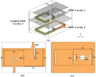
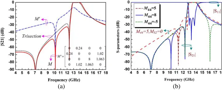
Figures 1(a), (b) and (c) show the three-dimensional view, top and middle metal layers of the proposed SIW filter, respectively. The corresponding topology is shown in Figure 2, and the corresponding coupling matrix M can be written as
⎡ ⎢ ⎢ ⎢ ⎢ ⎢ ⎣
0 MS1 MS2 0 0 0
MS1 M11 M12 M13 M14 0
MS2 M12 M22 M23 M24 0
0 M13 M23 M33 0 M3L
0 M14 M24 0 M44 M4L
0 0 0 M3L M4L 0
⎤ ⎥ ⎥ ⎥ ⎥ ⎥ ⎦
(1)
where diagonal elements in the coupling matrix are calculated by [22]:
Mi,i =f02−fi2 /(Δf ·fi) (2)
Here, parametersf0 and Δf are the central frequency and the bandwidth of the filter, respectively, and
fi is the resonant frequency of theith resonator. The bandwidth and central frequency of the filter are
(a)
(b) (c)
set to be 13.50 GHz and 1 GHz, respectively. Further, the generalized coupling matrix can be obtained using the gradient-based optimization method, and given by
M =
⎡ ⎢ ⎢ ⎢ ⎢ ⎢ ⎣
0 1.065 0.24 0 0 0
1.065 −0.23 0.701 0.66 0.0035 0 0.24 0.701 0.99 −0.701 0.012 0 0 0.66 −0.701 −0.23 0 1.02 0 0.0035 0.012 0 8 1.063
0 0 0 1.02 1.063 0
⎤ ⎥ ⎥ ⎥ ⎥ ⎥ ⎦
(3)
The resonator 4 in matrix (3) is taken as NRN, whose resonant frequency is far away from the central frequency of passband.
As shown in Figure 2(a), a trisection topology is given without introducing NRN. In Figure 2(b), we take nodes 3 and 4 as a singlet. If the source node in Figure 2(b) is replaced by nodes 1 and 2 in Figure 2(a), the proposed coupling scheme with NRN in Figure 2(c) can be obtained. The synthesized frequency dependentS-parameters, corresponding to the trisection, singlet and the coupling matrixM with different M44 are plotted in Figures 3(a) and (b).
S-parameters of the trisection and singlet are plotted in Figure 3(a). The black dotted line represents the S-parameter of trisection topology, whose coupling matrix is derived from matrix M without node 4. There are two TZs located at the lower stopband. For the singlet, the coupling matrix
M is derived from matrix M without nodes 1 and 2. Then, a TZ around 10 GHz is generated by the singlet M. Meanwhile, the synthesized S-parameter of matrix M is also plotted in Figure 3(a) for
(a) (b)
(c)
Figure 2. (a) The trisection, (b) the singlet, and (c) the topology of the proposed SIW filter.
(a) (b)
demonstrating the generation of three TZs. As shown in Figure 3(b), the TZ close to the passband is contributed to negative cross coupling in trisection topology. The lowest TZ is generated by coupling between source and cavity 2. The middle TZ is mainly controlled by the resonant frequency of NRN. If
M44>0, three transmission zeros are all located at the lower stopband. When M44<0, one TZ moves
from the lower to the upper stopband.
2.2. Filter Design
As shown in Figure 1, a folded-SIW cavity is introduced for realizing negative cross coupling and NRN. The folded-SIW cavity consists of a bottom metal layer, two dielectric layers, and in between a metal plate with a slot, a top conductor plane, and vias. It just likes a TE101 waveguide resonator is folded
along the thickness direction. The slot allows electromagnetic fields from one half to the other of the folded SIW cavity so that the mode can be maintained. To verify this, the electric field distributions of TE101 and TE201-modes in the folded-SIW cavity 3 are shown in Figures 4(a) and (b). For TE101
-mode, the electric field concentrates around the slot. Furthermore, the electric field of TE201-mode
reaches maximum at the center of folded-SIW cavity. TE101- and TE201-modes resonate around 11 GHz
and 13.5 GHz, respectively. All simulated results are performed by full-wave electromagnetic simulator (High Frequency Structure Simulator, HFSS).
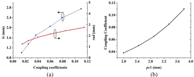
As shown in Figure 1(a), magnetic coupling between cavities 1 and 2 is obtained by two slots near vias, and a circular aperture is used to realize electric coupling between cavities 1 and 2. The coupling coefficients versus ls and rad are plotted in Figure 5(a), and the coupling will become larger with increasing of ls and rad. Two coupling iris are introduced to get couplings among cavities 1, 2 and 3. TE201-mode in folded-SIW cavity is taken as a resonator for passband implement. Therefore,
the signs of coupling coefficients M13 and M23 are different. Figure 5(b) plots the magnetic coupling
coefficients versuspc1. The coupling coefficients become larger with increase of pc1.
Figure 1(a) shows that two CPW probes are used to excite the SIW cavities 1 and 3. It should be noted that the circular aperture is also introduced to bring about the coupling between input probe and cavity 2. In the design, the magnetic coupling between cavities 1 and 2 should be much larger than
(a) (b)
Figure 4. The electric field distribution of the (a) TE101 and (b) TE201-mode in the third folded-SIW
cavity.
(a) (b)
the electric coupling. The simulated externalQ-factors for different values ofL1 andrad are plotted in
Figure 6. Qe1 and Qe2 are denoted as external factors of SIW cavities 1 and 2. As shown in Figure 6,
the external Q-factor of cavity 2 is large due to its weak coupling with input probe. As rad increases,
Qe2 will be smaller.
We use TE201-mode of folded-SIW cavity 3 to design the passband and regard TE101-mode as a
spurious resonance. For a singlet, the input and output coupling apertures can be arranged properly to get the required sign constraints on the coupling product. Therefore, it is possible to place the TZ below or above the passband [15]. The TE201-mode in the folded-SIW cavity is introduced to realize
negative cross coupling. Therefore, one TZ near the passband can be realized in the trisection topology. The TE101-mode in the folded-SIW cavity 3 serves as a singlet to produce the second transmission zero
around 11 GHz.
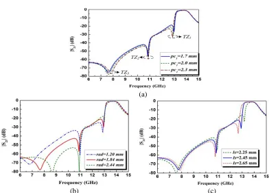
Figures 7(a), (b) and (c) plot the simulated S21-parameters of the proposed filter with different
Figure 6. The simulated external Q-factors of cavity 1 and 2.
(a)
(b) (c)
Figure 7. The simulated S21-parameter as a function of frequency for different values of (a) pc1,
(a) (b)
Figure 8. The simulated and measured S-parameters of the filter from (a) 1 GHz to 17 GHz, and (b) 1 GHz–28 GHz.
values ofpc1,rad andls, respectively. As shown in Figure 7(a), the location of TZ1 is mainly controlled
bypc1. The cross coupling will be larger with increase ofpc1, and TZ1will move close to the passband.
We can adjust the location of TZ3 by changing values of rad. As rad increases, the coupling MS2
becomes larger, and TZ3 will move close to the passband. In summary, TZ1 is contributed to the cross
coupling, and the lowest one TZ3 is generated by introducing MS2. The location of TZ2 is contributed
to resonant frequency of TE101-mode in SIW cavity 3.
As shown in Figure 1(c), electric and magnetic couplings both exist between SIW cavities 1 and 2. Electric coupling is obtained by the circular aperture etched on the middle metal layer, and the magnetic coupling is realized by slots around wall of via-holes. As plotted in Figure 7(b), the value of rad is fixed; the bandwidth increases with increase ofls; the position of TZ3 keeps unchanged.
3. RESULTS AND DISCUSSION
In order to validate our design, the third-order SIW filter sample was fabricated using multi-layer LTCC substrate. Its relative permittivity, loss tangent and thickness of each layer are 5.9, 0.0025 and 0.096 mm, respectively. The diameter of via-hole is 0.174 mm. Each SIW cavity occupies five LTCC layers. The geometrical parameters of the filter are listed as follows: L1 = 2.8 mm, L2 = 1.0 mm, L3 = 6.33 mm,
L4 = 6.33 mm,L5 = 6.4 mm,L6 = 6.3 mm, L7= 6.16 mm,L8= 6.16 mm, pc1 = 2.0 mm,pc2 = 2.9 mm,
rad= 1.85 mm, wid= 0.7 mm, ls= 2.45 mm.
A photograph of the fabricated SIW filter is given in Figure 8(a), the size of this filter is around 14×8 mm2, i.e., 1.55×0.9λ2g, whereλg is the guided wavelength at the central frequency. As shown in Figure 8(a), the measured center frequency and bandwidth of the SIW filter are around 13.88 GHz and 1 GHz, respectively. The slight shift of central frequency contributes to large shrink of SIW cavities. Besides, the measured insertion and return losses in the passband are 2.1 and better than 15 dB, respectively. Three transmission zeros (TZ1, TZ2 and TZ3) located at 13.1, 11 and 8 GHz are used to
get high rejection of the lower stopband. The circuit area is only 50% of a conventional planar SIW filters. The attenuated level is larger than 50 dB from DC to 10 GHz. Figure 8(b) shows the measured wideband performance. The spurious passband appears at 28 GHz, so we can say that better spurious suppression is achieved. This is due to the spurious passbands of SIW cavities 1, 2 are different from the counterparts of folded-SIW cavity 3.
4. CONCLUSION
In this paper, we present a compact third-order SIW LTCC filter with improved lower stopband performance. TE201-mode is not only taken as phase inverter, but also combines with TE101-mode
introduced to get high attenuation. Meanwhile, better spurious suppression performance is achieved. A filter sample was fabricated with multi-layer LTCC technology to validate the design.
ACKNOWLEDGMENT
This work was supported by the NSF under Grant KJ2011A007 and KJ2014A053 of Anhui Province, and by the NSF under Grant 51477001 of China.
REFERENCES
1. Deslands, D. and K. Wu, “Single-substrate integration technique of planar circuits and waveguide filters,”IEEE Trans. Microw. Theory Tech., Vol. 51, No. 2, 593–596, 2003.
2. Chen, X. P. and K. Wu, “Substrate integrated waveguide cross-coupled filter with negative coupling structure,” IEEE Trans. Microw. Theory Tech., Vol. 56, No. 1, 142–149, 2008.
3. Wang, R., L. S. Wu, and X. L. Zhou, “Compact folded substrate integrated waveguide cavities and bandpass filter,” Progress In Electromagnetics Research, Vol. 84, 135–147, 2008.
4. Wu, L., W. Shen, R. Qian, and X. W. Sun, “Design of substrate integrated waveguide (SIW) elliptic filter with novel coupling scheme,” Journal of Electromagnetic Waves and Applications, Vol. 26, Nos. 5–6, 827–835, 2012.
5. Shen, T. M., C. F. Chen, T. Y. Huang, and R. B. Wu, “Design of vertically stacked waveguide filters in LTCC,”IEEE Trans. Microw. Theory Tech., Vol. 55, No. 8, 1771–1779, 2007.
6. Chen, F., X. Q. Lin, X. X. Liu, K. J. Song, and Y. Fan, “A compact dual-band bandpass SIW filter,” Journal of Electromagnetic Waves and Applications, Vol. 27, No. 3, 338–344, 2013.
7. Zhang, Q. L., B. Z. Wang, W. Y. Yin, and L. S. Wu, “Design of a miniaturized dual-band double-folded substrate integrated waveguide bandpass filter with controllable bandwidths,” Progress In Electromagnetics Research, Vol. 136, 211–223, 2013.
8. Zhang, X. C., Z. Y. Yu, and J. Xu, “Novel band-pass substrate integrated waveguide (SIW) filter based on complementary split ring resonators (CSRRS),” Progress In Electromagnetics Research, Vol. 72, 39–46, 2007.
9. Jiang, W., W. Shen, L. Zhou, and W. Y. Yin, “Miniaturized and high-selectivity substrate integrated waveguide (SIW) bandpass filter loaded by complementary split-ring resonators (CSRRs),” Journal of Electromagnetic Waves and Applications, Vol. 26, Nos. 11–12, 1448–1459, 2012.
10. Zhang, Q. L., W. Y. Yin, S. He, and L. S. Wu, “Evanescent-mode substrate integrated waveguide (SIW) filters implemented with complementary split ring resonators,”Progress In Electromagnetics Research, Vol. 111, 419–432, 2011.
11. Ismail, A., M. S. Razalli, M. A. Mahdi, R. S. A. Raja Abdullah, N. K. Noordin, and M. F. A Rasid, “X-band trisection substrate-integrated waveguide quasi-elliptic filter,” Progress In Electromagnetics Research, Vol. 85, 133–145, 2008.
12. Wei, Q. F., Z. F. Li, W. J. Zhang, and J. F. Mao, “Three-pole cross-coupled substrate integrated waveguide (SIW) bandpass filters based on PCB process and multilayer LTCC technology,”
Microw. Opt. Tech. Lett., Vol. 51, No. 1, 71–73, 2009.
13. Potelon, B., J. F. Favennec, C. Quendo, E. Rius, C. Person, and J. C. Bohorquez, “Design of a substrate integrated waveguide (SIW) filter using a novel topology of coupling,” IEEE Microw. Wirel. Compon. Lett., Vol. 18, No. 9, 956–958, 2008.
14. Shen, W., W. Y. Yan, and X. W. Sun, “Compact coplanar waveguide-incorporated substrate integrated waveguide (SIW) filter,” Journal of Electromagnetic Waves and Applications, Vol. 24, No. 7, 871–879, 2010.
16. Chen, X. P. and K. Wu, “Self-packaged millimeter-wave substrate integrated waveguide filter with asymmetric frequency response,” IEEE Trans. Compon. Packag. Manufac. Tech., Vol. 2, No. 5, 775–782, 2012.
17. Chen, X. P., K. Wu, and D. Drolet, “Substrate integrated waveguide filter with improved stopband performance for satellite ground terminal,” IEEE Trans. Microw. Theory Tech., Vol. 57, No. 3, 674–683, 2009.
18. Zhang, Z. G., Y. Fan, Y. J. Cheng, and Y. H. Zhang, “A compact multilayer dual-mode substrate integrated circular cavity (SICC) filter for X-band application,” Progress In Electromagnetics Research, Vol. 122, 453–465, 2012.
19. Shen, W., L. S. Wu, X. W. Sun, W. Y. Yin, and J. F. Mao, “Novel substrate integrated waveguide filters with mixed cross coupling (MCC),” IEEE Microw. Wirel. Compon. Lett., Vol. 19, No. 11, 701–703, Nov. 2009.
20. Xu, Z. Q., Y. Shi, C. Y. Xu, and P. Wang, “A novel dual mode substrate integrated waveguide filter with mixed source-load coupling (MSLC),” Progress In Electromagnetics Research, Vol. 136, 595–606, 2013.
21. Wu, L. S., J. F. Mao, W. Shen, and W. Y. Yin, “Extended doublet bandpass filters implemented with microstrip resonator and full-/half-mode substrate integrated cavities,”Progress In Electromagnetics Research, Vol. 101, 203–216, 2010.