dynamics and nonlinear eects
Thesis by
Yaakov (Yasha) Vilenchik
In Partial Fulllment of the Requirements for the Degree of
Doctor of Philosophy
California Institute of Technology Pasadena, California
2015
c 2015
Acknowledgments
These last few years at Caltech have been a time of immense personal and intellectual growth for me. I would like to take the opportunity to thank the many people I've learned from and with.
First and foremost, I would like to thank and acknowledge my advisor, Professor Amnon Yariv. Professor Yariv provided me with the opportunity to work at the forefront of science, and has succeeded in convincing me that nothing is impossible. His guidance has shaped me into a researcher who strives to combine a top-level scientic bird's-eye-view, with a down-to-earth understanding of technical challenges. I deeply appreciate the time and eort of my thesis committee members, Professors Kerry Vahala, Oskar Painter and Andrei Faraon. This committee is truly the dream team for my thesis, and I am very privileged to have them in my corner.
I would like to thank Professor Bruno Crosignani for his support and encourage-ment over the years. His unique approach to problem-solving in all eld from physics to politics and philosophy has deeply enriched me and made me a better researcher and critical thinker.
and his input was crucial time after time. Our collaboration has yielded an order of magnitude improvement in both the characterization setup, and my experimental skills. I must thank Dongwan Kim for his help in the fabrication eort, and for our many conversations which helped me to constantly improve my understanding of every aspect of this project. I would also like to thank Mark Harfouche for his frequent advice, that always provided me with new insights. This project beneted a lot from his wide range of expertise, that never ceased to amaze me. Other members of the Yariv group Jacob Sendowski, Arseny Vasilyev, Sinan Zhao, Xiankai Sun, Hsi-Chun Liu, Avi Zadok, Paula Popescu and Marilena Dimotsantou have all contributed to this work, each in their unique way, and for that I am thankful. A special thanks goes to group-members in the broader sense, Reg Lee and George Rakuljic, for their useful input and advice.
The sta members at KNI were a source of both knowledge and help. The sup-port and advice I got from Guy DeRose, Melissa Melendes and Steven Martinez was indispensable. I would like to thank Christy Jenstad and Mabel Chik for helping me to navigate life and research at Caltech. I would especially like to thank Connie Ro-driguez, who enabled me to do science, without needing to worry about the immense amount of paperwork. She made sure that my environment never got too cold, too warm or too loud both literally and metaphorically.
The Israeli community at Caltech has provided an important support net, and helped me transition smoothly to a new country and culture. My time at Caltech would not have been as vibrant without them. I also thank Chabad of Pasadena and the Pasadena Jewish Community for enriching my spiritual life here.
Abstract
Narrow-linewidth lasers play an important role in a wide variety of applications, from sensing and spectroscopy to optical communication and on-chip clocks. Cur-rent narrow-linewidth systems are usually implemented in doped bers and are big, expensive, and power-hungry. Semiconductor lasers compete favorably in size, cost, and power consumption, but their linewidth is historically limited to the sub-MHz regime. However, it has been recently demonstrated that a new design paradigm, in which the optical energy is stored away from the active region in a composite high-Q resonator, has the potential to dramatically improve the coherence of the laser.
This work explores this design paradigm, as applied on the hybrid Si/III-V plat-form. It demonstrates a record sub-KHz white-noise-oor linewidth. It further shows, both theoretically and experimentally, that this strategy practically elimi-nates Henry's linewidth enhancement by positioning a damped relaxation resonance at frequencies as low as 70 MHz, yielding truly quantum limited devices at frequencies of interest.
In addition to this empirical contribution, this work explores the limits of perfor-mance of this platform. Here, the eect of two-photon-absorption and free-carrier-absorption are analyzed, using modied rate equations and Langevin force approach. The analysis predicts that as the intra-cavity eld intensity builds up in the high-Q resonator, non-linear eects cause a new domain of performance-limiting factors. Steady-state behavior, laser dynamics, and frequency noise performance are exam-ined in the context of this unique platform, pointing at the importance of nonlinear eects.
Contents
Acknowledgments iii
Abstract v
1 Introduction 1
1.1 Narrow-linewidth semiconductor lasers . . . 2
1.2 Laser sources for coherent communication . . . 5
1.3 Linear and non-linear performance limiting factors . . . 6
2 Hybrid Si/III-V as a platform for narrow linewidth 9 2.1 Noise in conventional semiconductor lasers . . . 10
2.2 Hybrid Si/III-V platform . . . 14
2.3 Noise reduction in hybrid Si/III-V . . . 16
2.3.1 High-Q silicon resonator . . . 16
2.3.2 Modal gain and loss . . . 17
2.3.2.1 General description . . . 18
2.3.2.2 The spacer lasers . . . 20
2.3.3 Schawlow-Townes linewidth . . . 21
3 Non-linear eects in hybrid Si/III-V 24 3.1 Two-photon-absorption in silicon . . . 26
3.2 Free-carrier-absorption . . . 28
3.2.1 General methodology . . . 30
3.2.3 Surface recombination . . . 32
3.2.4 Carrier diusion . . . 34
3.2.5 Eective carrier lifetime . . . 35
4 Modied rate equations 40 4.1 Flat-mode approximation . . . 40
4.2 Working with densities or total numbers? . . . 42
4.3 Pump . . . 43
4.4 Linear loss . . . 44
4.5 Gain . . . 45
4.5.1 The quantum-well: a two or three dimensional creature? . . . 45
4.5.2 Active connement factor . . . 46
4.5.3 Material gain . . . 47
4.6 Spontaneous emission . . . 47
4.6.1 Model for the population inversion factor . . . 48
4.7 Two-photon-absorption . . . 49
4.8 Spontaneous recombination in the QW . . . 50
4.9 Rate equation for free-carriers in silicon . . . 51
4.10 Free-carrier-absorption . . . 52
4.11 Total loss rate . . . 52
4.12 The modied rate equations . . . 53
5 Steady-state operation - Theoretical analysis 55 5.1 Steady-state carrier density in silicon . . . 55
5.2 Gain saturation . . . 56
5.3 Threshold current . . . 56
5.4 Output power . . . 58
5.4.1 Wall-plug eciency . . . 58
5.4.2 L-I curve . . . 59
5.4.3 Slope eciency . . . 61
6 Steady-state operation - Experimental results 68
6.1 Threshold current . . . 69
6.2 L-I curves . . . 71
6.3 Schawlow-Townes noise oor . . . 73
7 Dynamic operation - Theoretical analysis 77 7.1 Small-signal analysis . . . 77
7.2 Intensity modulation response . . . 79
7.2.1 Analytical investigation . . . 81
7.2.1.1 Low nonlinear loss regime: . . . 82
7.2.1.2 High nonlinear loss regime: . . . 83
7.2.2 Numerical investigation . . . 84
7.3 Frequency modulation response . . . 86
7.3.1 Eect of Quantum Well carriers . . . 89
7.3.1.1 Gain compression . . . 89
7.3.1.2 Henry's alpha parameter . . . 90
7.3.1.3 Frequency modulation response curve . . . 91
7.3.2 The eects of free-carriers in silicon . . . 92
7.3.2.1 Plasma eects in silicon . . . 93
7.3.3 The total frequency chirp . . . 94
8 Dynamic operation - Experimental results 99 8.1 Intensity modulation response . . . 99
8.2 Frequency modulation response . . . 105
9 Noise performance - Theoretical analysis 110 9.1 Methodology - Langevin noise sources . . . 111
9.2 Source of noise - uctuations . . . 112
9.2.1 Photon density . . . 116
9.2.2 Carriers in the quantum wells . . . 119
9.2.4 Temperature . . . 122
9.3 Frequency noise . . . 124
9.3.1 Spontaneous emission . . . 125
9.3.2 Henry's linewidth enhancement . . . 126
9.3.3 Noise due to the plasma eect in silicon . . . 127
9.3.4 Noise due to the thermo-optic eect in silicon . . . 131
9.3.5 Total noise spectrum . . . 133
10 Noise performance - Experimental results 138 11 Conclusion 144 11.1 Summary of key results . . . 144
11.2 Future directions . . . 146
Bibliography 149 A Fabrication process 165 A.1 Silicon processing . . . 165
A.1.1 Chrome deposition . . . 165
A.1.2 Lithography . . . 168
A.1.3 Etch . . . 168
A.1.4 Oxidation . . . 169
A.2 Wafer bonding . . . 169
A.2.1 Surface treatment . . . 170
A.2.2 Bonding . . . 170
A.2.3 Substrate removal . . . 170
A.3 III-V processing . . . 172
A.3.1 Ion implantation . . . 172
A.3.2 P-metal deposition . . . 172
A.3.3 Mesa formation . . . 173
A.3.4 N-Metal deposition . . . 175
B Characterization setups 177
B.1 Mounting and probing the lasers . . . 178
B.1.1 Mounting of laser bars . . . 178
B.1.2 Thermal management . . . 178
B.2 L-I curves . . . 179
B.2.1 CW excitation . . . 179
B.2.2 Pulsed excitation . . . 179
B.3 Intensity modulation response . . . 180
B.3.1 Setup and equipment . . . 180
B.3.2 Calibration and measurement procedures . . . 181
B.3.2.1 Photodetector response . . . 181
B.3.2.2 Driving circuitry response . . . 181
B.3.2.3 Calculating the small-signal current . . . 182
B.3.2.4 Delay compensation . . . 183
B.4 Frequency modulation response . . . 183
B.4.1 Setup and equipment . . . 183
B.4.2 Calibration and measurement procedure . . . 185
B.4.2.1 Balancing photodetectors . . . 185
B.4.2.2 Photodetector response . . . 186
B.4.2.3 Voltage swing . . . 186
B.4.2.4 Delay compensation . . . 188
B.4.2.5 Measurement procedure . . . 188
B.4.2.6 Calculating the frequency response from the measure-ment . . . 189
B.5 Frequency noise spectrum measurement . . . 191
B.5.1 Setup and equipment . . . 192
B.5.2 Calibration and measurement procedures . . . 192
B.5.2.1 Balanced PD and amplier . . . 192
List of Figures
1.1 Constellation diagrams. (a) Binary Amplitude Phase Shift Keying (b) 16 Quadrature Amplitude Modulation. . . 5 1.2 Phasor diagram demonstrating the eect of a spontaneous emission
event . . . 8
2.1 Hybrid Si/III-V laser schematics . . . 15 2.2 Band structure of the mode-gap resonator. The parabolic potential-well
supports one optical mode . . . 17 2.3 (a) Quality factor of hybrid Si/III-V composite resonator (b) Mode
pro-le of a traditional III-V laser (c) Propro-le of a high-Q hybrid Si/III-V laser . . . 19 2.4 Connement in III-V and in QWs vs. spacer thickness . . . 21
3.1 Schematic description of two-photon-absorption . . . 25 3.2 Model for FCA in silicon. Model #1 by [58, 101]. Model #2 by [70] . . 29 3.3 Waveguide structure used for analysis of FCA . . . 30 3.4 Model for the ambipolar diusion coecient of silicon . . . 35 3.5 Carrier density prole for several dierent surface recombination proles 36 3.6 Eective lifetime of carrier in silicon for S=1cm
sec . . . 37
3.7 Eective lifetime of carriers in Si (low photon excitation regime) . . . . 38
4.3 Comparison between dierent loss mechanisms vs. photon density. Qsi =
106, typical absorption in III-V is assumed (i.e., 10cm−1), connement factor in III-V of 1% and eective lifetime of carriers in Si ofτef f = 30ns. 53
5.1 Threshold current vs. connement factor in III-V for dierent quality factors of the Si resonator . . . 57 5.2 Eciency (left axis) and total Q (right axis) vs. mirror Q. Qintsi = 106 ;
ηi = 1 ; IItr = 10 (a) 30nm spacer (b) 100nm spacer (c) 150nm spacer . 60
5.3 Eciency of dierent spacer design vs. total-Q . . . 61 5.4 L-I curves for dierent values of connement factors with and without
nonlinear eects for Qintsi = 106 (a) spacer 150nm (b) spacer 100nm (c) spacer 30nm . . . 62 5.5 Normalized slope eciency at I = 4·Ith . . . 63
5.6 Schawlow-Townes linewidth vs. connement in III-V for dierent silicon resonators, with and without nonlinear eects at I = 4·Ith . . . 65
5.7 Impact of nonlinear eects on linewidth for changing quality factors. Calculated at I = 5·Ith . . . 66
5.8 Impact of nonlinear eects on linewidth for changing pump current. Calculated at I = 5·Ith for QSi= 106 . . . 66
6.1 Threshold current for dierent spacer designs. (a) 1560nm lasers (b) 1575nm lasers . . . 70 6.2 Normalized L-I curves for three spacer designs. The non-normalized
output powers at I=150mA are: 0.89mW, 0.62mW, and 10.2mW for the 200nm, 100nm, and 30nm spacers, respectively . . . 72 6.3 L-I curves of the 150nm spacer. (a) For varying stage temperatures (b)
In pulsed operation (duty cycle = 1%) . . . 74 6.4 Schawlow-Townes linewidth vs current oset from threshold for the three
7.1 Intensity modulation response curves with and without nonlinear eects.
I = 4Ith, QSi= 106 (a) 30nm spacer (b) 100nm spacer (c) 150nm spacer 85
7.2 Intensity modulation response curves for dierent spacer thicknesses.
I = 4Ith, QSi= 106 (a) amplitude (b) phase . . . 87
7.3 Intensity modulation response curves for dierent spacer thicknesses.
I = 10Ith, QSi= 106 (a) amplitude (b) phase . . . 88
7.4 Frequency modulation response due to quantum well electrons for dif-ferent values of spacer thickness. αH = 7,I = 2·Ith, QSi= 106 . . . . 91
7.5 Frequency modulation response due to free carriers in silicon for dierent values of spacer thickness. αH = 7, I = 2·Ith,QSi = 106 . . . 94
7.6 Frequency modulation response for several dierent spacer thicknesses, with and without nonlinear eects for αH = 7, I = 2·Ith, QSi = 106 .
(a) 30nm spacer (b) 100nm spacer (c) 150nm spacer . . . 95 7.7 Frequency modulation response for several dierent spacer thicknesses
for αH = 7,I = 2·Ith, QSi= 106 . . . 96
7.8 Eect of pump current on frequency modulation response for two dier-ent spacer thicknesses αH = 7, I = 2·Ith, QSi = 106. (a) 30nm spacer
(b) 150nm spacer . . . 97
8.1 Intensity modulation response of 30nm spacer laser (Chip 1, bar 5, Slot 1, device 7) for dierent bias currents. 3.5mA current modulation. Mea-sured with New-Focus 1544B photodetector and HP 8722C RF network analyzer (a) Normalized magnitude (b) Phase . . . 101 8.2 Intensity modulation response of 100nm spacer laser (chip 1, bar 1, slo
8.3 Intensity modulation response of 150nm spacer laser (chip 1, bar 1, slot 2, device 19) for dierent bias currents. 3.3mA current modulation. Measured using New-Focus 1544B photodetector and Agilent 4395A net-work analyzer (a) Normalized magnitude (b) Phase . . . 103 8.4 Intensity modulation response (magnitude in a.u.) of dierent spacer
lasers for pump current oset of 40mA. . . 104 8.5 Frequency modulation response of 30nm spacer laser (Chip 1, bar 5, Slot
1, device 7) for dierent bias currents. 0.1mA current modulation. Mea-sured with Optilab BPR-20-M balanced photodetector and HP 8722C RF network analyzer, using MZI with FSR = 7.06GHz . . . 105 8.6 Frequency modulation response of 100nm spacer laser (Chip 1, bar 1,
Slot 2, device 19) for dierent bias currents. 35nA current modulation. Measured with Optilab BPR-20-M balanced photodetector MZI with FSR = 1.56GHz. Low frequencies (<500 MHz) were measured using Agilent 4395A network analyzer and high frequencies (>500MHz) using HP 8722C analyzer. Curves from the two analyzers are plotted together without any additional post-processing (stitching) . . . 106 8.7 Frequency modulation response of 150nm spacer laser (Chip 1, bar 1,
Slot 2, device 19) for dierent bias currents. 0.1mA current modulation. Measured with Optilab BPR-20-M balanced photodetector and Agilent 4395A network analyzer, using MZI with FSR = 1.56GHz . . . 106 8.8 Frequency modulation response of dierent spacer lasers for pump
cur-rent oset of 50mA. . . 107
9.1 Particle reservoir picture of the system . . . 113 9.2 PSD of the photon density (150nm spacer,QSi = 106, I = 4Ith) (a)
9.3 Comparison of the dierent terms of the PSD of QW-carrier density (150nm spacer, QSi = 106, I = 4Ith) . . . 119
9.4 Noise spectrum of silicon carrier density for shot-noise model (150nm spacer, QSi= 106, I = 4Ith) . . . 120
9.5 Frequency noise due to spontaneous emission and QW carrier density uctuations using Langevin shot-noise model. QSi = 106, I = 4Ith,
αH = 3 . . . 127
9.6 The eect of Si-carrier uctuation on the frequency noise spectrum: Eective recombination model vs recombination-diusion model. 150nm Spacer, QSi= 106, I = 2Ith . . . 129
9.7 Frequency noise spectrum due to Si carrier uctuations for dierent pump currents. 150nm Spacer, QSi= 106 . . . 130
9.8 Frequency noise spectrum due to Si carrier uctuations for dierent spacers. QSi= 106, I = 2·Ith . . . 131
9.9 The dierent components of the frequency noise spectrum due to tem-perature uctuations (150nm spacer, QSi = 106, I = 2·Ith ) . . . 133
9.10 Frequency noise related to temperature uctuations for dierent spacer designs (QSi= 106, I = 2·Ith ) . . . 134
9.11 The dierent components of the total frequency noise spectrum (QSi =
106, I = 2·Ith ). (a) 150nm spacer (b) 100nm spacer (c) 30nm spacer . 135
9.12 Predicted frequency noise spectrum of dierent spacer designs (QSi =
106, I = 2·Ith ) . . . 136
9.13 Predicted frequency noise spectrum for the 150nm spacer designs at dierent pump powers (QSi= 106) . . . 136
10.3 Frequency noise spectrum vs. pump current for dierent spacer designs (a) 150nm spacer (threshold @ 66mA) (b) 100nm spacer (threshold @ 28mA) (c) 30nm spacer (threshold @ 55mA) . . . 141 10.4 Frequency noise spectrum for dierent spacer designs at I−Ith= 33mA 142
A.1 Spacer laser device Schematics . . . 166 A.2 Flow diagram of the silicon processing steps . . . 167 A.3 Flow diagram of the III-V processing steps . . . 172 A.4 SEM images of mesa formed using the two mask process (a) Entire mesa
and Si waveguide (b) Sidewalls of mesa and InGaAs layers (c) Etch and under-cut of the QW layer . . . 175
B.1 Schematics of L-I curve characterization setup . . . 179 B.2 Schematics of the experimental setup used for intensity modulation
re-sponse measurements . . . 180 B.3 Measured response of NF1544B photodetector. The PD response was
subtracted from measured laser response . . . 182 B.4 Schematics of the experimental setup used for frequency modulation
response measurements . . . 184 B.5 Schematics of the electronic feedback PCB used to lock the MZI to
quadrature . . . 185 B.6 Response curves of balanced PDs (a) New Focus 1817 (b) Optilab BPR
20-M . . . 187 B.7 Schematics of the experimental setup used for frequency noise spectrum
measurements . . . 193 B.8 Intensity noise measured for dierent input powers by the balanced
pho-todetector (Optilab BPM-20) . . . 194 B.9 Intensity noise vs calculated dark+shot noise for dierent input power
List of Tables
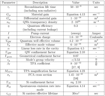
4.1 Parameters used for rate equations . . . 54
A.1 Device dimensions. Notations is based on Figure A.1 . . . 166
A.2 III-V wafer structure . . . 167
A.3 Conditions of Cr evaporation . . . 168
A.4 Steps for E-Beam lithography . . . 168
A.5 ICP etch steps and conditions . . . 169
A.6 Oxidation/Anneal steps and conditions . . . 170
A.7 Steps and conditions for wafer bonding . . . 171
A.8 Substrate removal steps and conditions . . . 171
A.9 Parameters used for ion implantation . . . 173
A.10 Steps and conditions used to deposit P metal stack . . . 174
A.11 Steps and conditions for lift-o photo-lithography . . . 174
A.12 steps and conditions used to form the mesa . . . 175
Chapter 1
Introduction
For decades, semiconductor lasers have been considered reliable, inexpensive everyday light sources. However, they lack high quality coherence properties. On the other hand, narrow-linewidth lasers, i.e., ber or solid-state devices, have been considered exotic, bulky, and expensive. A new technology the hybrid Si/III-V platform [75]; and a new laser design paradigm [106], were recently combined to demonstrate a record narrow-linewidth semiconductor laser [88]. This demonstration might be the rst milestone towards the penetration of semiconductor lasers to the narrow-linewidth laser industry, with a potentially dramatic impact on the narrow-narrow-linewidth industry.
Work pioneered by John Bowers et al. (i.e., [76, 75, 113, 34]) has enabled the integration of direct-bandgap semiconductor devices with a low-loss material, mainly silicon. The work by Amnon Yariv et al. (i.e., [132, 88]) used this platform to demonstrate a hybrid Si/III-V laser with 18 KHz white-noise oor linewidth. The mechanism of noise reduction was further developed by Yariv et al., who portrayed a path towards further reduction [106]. However, experimental results in that work were inconclusive, and did not overcome the ∼18 KHz barrier.
1. It provides a conclusive experimental validation for the new design approach - experiments demonstrating a record sub-KHz linewidth are presented in this work for the rst time. A conclusive linewidth reduction trend is also presented, portraying the path for further improvement.
2. A theoretical analysis and experimental results of laser dynamics of this unique platform are also presented in this work for the rst time. Intensity and fre-quency modulation response measurements were performed, showing unique characteristics of the hybrid platform, i.e., relaxation resonance frequencies as low as 100 MHz.
3. It provides a theoretical model and experimental validation of the impact of nonlinear eects, i.e., two-photon-absorption and the attendant free-carrier-absorption on laser performance. It is shown that as the intra-cavity intensity builds up these nonlinear processes limit the achievable linewidth and alter the laser dynamics. Others have shown that free-carrier-absorption in Si aects device performance [85, 57, 37, 112, 133]. However, this is the rst time these eects are considered and experimentally demonstrated in the context of high-Q Si-based lasers. The analysis in this work provides a limit to the achievable device performance, and also oers directions to overcome these limits in silicon.
1.1 Narrow-linewidth semiconductor lasers
Semiconductor lasers (SCLs), in the context of this work, are high-coherence light sources constructed using direct band-gap semiconductor materials. These lasers can be pumped either optically or electrically. However, the main advantage of SCLs is their ability to be pumped electrically using standard current sources. For this reason, in the remainder of this work I will assume electrical pumping whenever SCLs are described. SCLs have many other advantages: they are lightweight, ecient in converting electrical energy into optical energy, and inexpensive, as well as have a small footprint. They can also be easily integrated with other electronic components to allow for control and manipulation of the laser eld. However, the coherence properties of SCLs are usually inferior in comparison to other laser platforms, such as ber lasers, solid-state lasers or gas lasers. The linewidth of SCLs is historically limited to the sub-MHz regime. The reasons for that will be described in detail in Chapter 2.
Narrow-linewidth lasers have been used in many elds. High-coherence light sources are so useful since there are many systems in which the narrow-linewidth sources translate directly into high-resolution. For example, in an interferometric ranging experiment high coherence translates into superior depth resolution. In spec-troscopy, narrow-linewidth operation results in higher spectral resolution. In atomic clocks that are based on coherent population trapping (CPT), low-noise operation is essential for good temporal resolution of the clock.
To understand the basis behind this linewidth-resolution relationship it is useful to refer to a simple experiment: the Mach-Zehnder interferometer (MZI). Consider a laser beam (assume perfect spatial coherence for simplicity) that is split into two arms. One arm is delayed by a time delay of τ compared to the other, and the
two beams are then combined and detected on a photodetector (PD). Assume the detected signal is measured for a time period much longer than the coherence time, such that the signal Fourier-limited width is much narrower than the linewidth of the laser. Neglecting amplitude noise, the complex laser eld can be expressed as:
The power at the PD can be written as (assume equal power and polarization in both arms):
P(t) = 1
4|E(t) +E(t−τ)|
2 = A2
2 (1 +cos(ωτ +δφ(t)−δφ(t−τ))) (1.2)
If we assume for simplicity that the constant phase term is biased such that ωτ = 2πm+π2, wherem is an integer, we get
P(t)≈ A
2
2 (1 + ∆φ(t, τ)) (1.3)
where we have dened
∆φ(t, τ) =δφ(t)−δφ(t−τ) (1.4)
and assumed∆φ(t, τ)π. The power spectral density (PSD) of the stationary and
stochastic phase change term ∆φ is related to the PSD of the laser frequency noise Wφ˙ by [78]:
W∆φ=Wφ˙sin
2(ωτ /2)
(ω/2)2 (1.5)
Assuming a white frequency noise, the phase change can be found analytically by integration [78]:
<∆φ(t, τ)2 >=Wφ˙τ (1.6)
It can be seen from 1.6 and 1.5 that the noise at the PD output scales with the laser frequency noise. If, for example one wishes to detect small changes of the optical delay τ, the laser's noise term will eventually limit the achievable resolution. The
(a) (b)
Figure 1.1: Constellation diagrams. (a) Binary Amplitude Phase Shift Keying (b) 16 Quadrature Amplitude Modulation.
1.2 Laser sources for coherent communication
Semiconductor lasers have been driving the optical communication industry for several decades. Direct (intensity) modulation is the most common modulation scheme. However, as the demand for data increases rapidly, phase modulation schemes gain popularity. Among other advantages, phase modulation scheme can pack more bits per symbol, hence increasing the data content eciency of the channel. The concept of high data content per symbol is demonstrated in Figure 1.1. The bit error rate will be a function of the phase noise accumulated within one modulation period [134] and the distance between two consecutive states on the phasor diagram. In the realm of communication networks, this puts a linewidth requirement for the laser source, for a given modulation scheme.
noise, wφ˙, if τ is smaller. These two competing trends merit some discussion when
trying to evaluate the requirements from future optical communication light sources. The increase in modulation speed is mostly driven by advances in the miniatur-ization of light modulators. Low capacitance is often required and sets a demand for smaller footprints devices. On the other hand, the increase of data rate by packing more bits per symbol is driven by advancements in digital signal processing (DSP). Faster parallel electronics is needed to encode multi-bit signals. This in turn is also driven by progress in high-speed electronics. These two market trends, faster mod-ulators and faster DSPs, often go hand in hand. In the context of light sources for future optical communication networks, this means that the rate of increase in demand for narrower linewidth lasers for telecom should stagnate somewhat due to these competing trends.
The argument above implies that in the near future, it might not be necessary to portray a fast path towards constant reduction of laser linewidth. However, today's semiconductor lasers are incompatible with the transition to coherent communication, requiring alternative solutions. For example [94], to transmit 64 bits per symbol at frequency of 20 GHz, while requiring Bit Error Rate (BER) of 10−4 and sensitivity
penalty of 2dB using feed-forward phase estimation techniques would require a laser with linewidth of 1.2 KHz. Today's state of the art DFB lasers that are commonly employed in communication networks are limited to a linewidth of about 100 KHz. Therefore, an improvement of about 2 orders of magnitude in linewidth is required to support near-future coherent communication.
1.3 Linear and non-linear performance limiting
fac-tors
suppression, and wall plug eciency are often as important, for practical reasons. Laser linewidth, or noise, are fundamentally related to losses. Here I refer to loss in the broader sense by dening it as a mechanism that couples useful energy laser mode electromagnetic energy or pump electrical energy to a thermal bath or a continuum of modes. For example, optical loss through scattering couples the mode to the free-space continuum. Dissipation through resistive heating couples pump current to the thermal bath. A very fundamental theorem, the uctuation-dissipation theorem, relates the uctuation-dissipation through these channels to uctuations in the cavity. This theorem implies that the same mechanism that couples energy to the outside world also couples uctuation from the outside world to the cavity.
Despite the universal nature of the uctuation-dissipation theorem, it is not very useful for describing laser noise in a quantitative way. Text-book laser theory usually attacks noise by engaging the specic physics of a laser system. Losses in the cavity force us to pump the laser harder, such that gain overcomes loss. This in turn will yield larger density of excited electrons. These excited electrons will relax randomly to the ground state, adding random phase to the laser eld through the process of spontaneous emission. In this case, the relaxation of excited electrons to the ground state is due to the interaction with the vacuum state corresponding to the laser mode and not the free-space continuum. This approach can be shown to be directly related to the the uctuation-dissipation theorem [52].
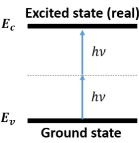
In addition to uctuations, losses limit the amount of energy we can store in the cavity. The addition of random phase through spontaneous emission will add noise to the laser eld, and will have bigger impact if there are fewer stored photons. This is demonstrated in the phasor diagram of Figure 1.2. No matter which approach or argument is used to calculate the exact noise characteristics, it is obvious that loss is a fundamentally root cause of noise or uctuations. We will divide loss mechanisms into two categories:
Figure 1.2: Phasor diagram demonstrating the eect of a spontaneous emission event
linear loss can be described through the equation:
dI
dt =−αI (1.7)
where I is a generic quantity, e.g., photon density or EM energy. The decay in
this case is exponential with a rate that depends only on the constant α.
2. Non-linear loss: this loss refers to a mechanism in which the decay rate α
depends on the quantity I through some non-constant function:
dI
dt =−α(I)·I (1.8)
In the context of this work, non-linear loss refers to optical losses that depend on the photon density itself. Despite the more complex nature of this loss mechanism, the same arguments implied in the uctuation-dissipation theorem are valid, and non-linear loss will have an impact on laser coherence.
Chapter 2
Hybrid Si/III-V as a platform for
narrow linewidth
Semiconductor lasers are notorious for their low coherence properties. Despite the tremendous progress in micro fabrication and wafer growth this limit has hardly been broken. Some of the more successful attempts include a 64 KHz laser [32], a 28 KHz laser [38], and a 3.6 KHz laser [71]. Common to these results is the implementation of a large-mode-area, small connement factors, and low-loss cavities. In [71] linewidth improvement was achieved also by suppression of spectral hole burning.
As we shall see in this chapter a key requirement for linewidth suppression is the reduction of modal loss. However, semiconductor lasers based on common III-V epistructures require high density of dopants and carriers to maintain a low resistance current path for carrier injection into the quantum wells (QW). The high carrier den-sity interacts with the mode and induces extra loss through radiation and dissipation. The fact that the III-V-only platform requires current path through the same volume in which the optical mode is stored renders this platform inconsistent with low-loss. Even though some improvement can be made for III-V lasers by decreasing QW connement and reducing losses elsewhere, this platform is inherently limited.
(UCSB), the hybrid Si/III-V platform [75] opened up a path to narrow linewidth semi-conductor lasers. This path was followed by researchers from Caltech [88], demon-strating 18 KHz lasers. The work by Yariv et al. has portrayed a path towards further linewidth reduction on this platform. However, experimental results [106] were inconclusive . In this work I will provide theory describing the limits of per-formance of this platform and conclusive experimental results supporting the theory and demonstrating record-breaking performance.
2.1 Noise in conventional semiconductor lasers
There is a vast amount of research on the physics of noise in semiconductor lasers. [131] attacks the problem from fundamental quantum mechanics, [13] has a nice cussion on some phenomenological aspects of noise analysis, [78] have a detailed dis-cussion on characterization and measurement of noise in lasers. Detailed derivations of semiconductor noise is outside the scope of this work. However, it is important to understand a few key concepts and results.
The electromagnetic laser eld has magnitude and phase. In general, noise can appear in both. In common laser systems amplitude noise is vastly suppressed by gain saturation, providing a restoring force for the laser amplitude. In fact, in many practical laser systems, amplitude noise is at or very close to the shot-noise limit. On the other hand, the phase of the electromagnetic eld doesn't have the same restoring force. Laser phase is uctuating in a random walk process. For this reason, for most applications laser noise is dominated by phase noise. Thus, in this work I will refer to phase noise as laser noise, unless otherwise stated.
Laser frequency noise spectrum has several components. Equation 2.1 can be used to describe it in a general way:
Wφ˙ =
∞
X
i=1
ai
fi +C (2.1)
noise terms can be traced to several mechanisms. Some of them tend to be technical (e.g., mechanical vibration of the stage), and some of them are more fundamental (e.g., thermal diusion). A nice review of generic 1/f noise can be found in [66]. Due to the illusive nature of these 1/f noise terms they are often treated as technical noise. In this work I will use the same notation even though in some cases the source of this noise could be fundamental. The constant C of the second term in Equation 2.1 is referred to as Schawlow-Townes white noise oor. In most semiconductor lasers, this term becomes dominant over 1/f terms at frequencies as low as few KHz. For this reason, laser noise analysis often emphasizes this white noise oor level. The ideas and strategies laid out in this chapter will focus on the reduction of this dominant term.
The analysis of white noise in semiconductor lasers can be laid out in several steps:
1. The main source of noise in SCLs is spontaneous emission. This refers to the stochastic radiative decay of excited electrons to the ground state. Every spon-taneous emission event adds on the average one photon to the laser mode [31]. The eld of this photon has a random phase compared to the laser coherent eld and is thus source of phase uctuations. The lack of restoring force for the laser's phase means that over time the phase will go through a random walk process. The mean square of the phase deviation will be proportional to observation time τ. If the frequency noise is white (setting ai = 0 in Equation
2.1 ) the mean square of the phase deviation will follow Equation 1.6.
2. Above laser threshold the modal gain of the laser is clamped at the modal loss level. A gain term that is exceeding the losses would imply the unphysical situation of diverging exponential photon density. In fact, due to spontaneous emission, the gain is only approaching losses from below; however, for any practical purposes we can set them as equal:
Here Gm is material gain in units of sec−1 and is a function of both the
las-ing frequency ν and the density of excited electrons n . Γ is the connement coecient that describes the connement of optical energy in the active (gain) region, such thatΓGm is the modal gain. αdescribes modal loss in inverse time
units. This includes intrinsic loss due to absorption and scattering, but also external mirror loss.
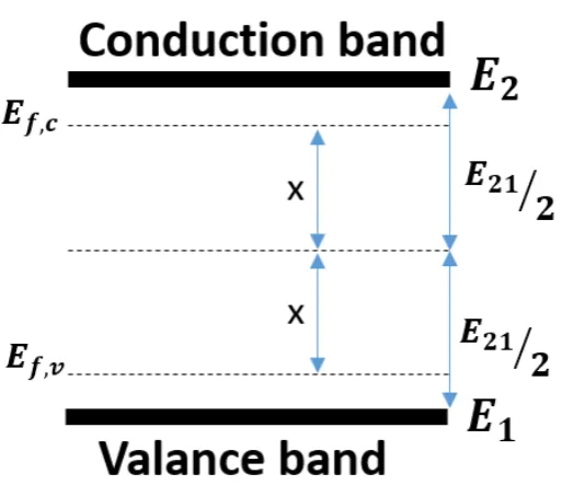
3. There is a fundamental relationship between stimulated and spontaneous emis-sion. The gain, or stimulated emission rate, depends on the level of population inversion, i.e., the dierence between the density of excited electrons and ground state electrons. The spontaneous emission process depends only on that of the number of excited electrons. The inversion level and the density of excited car-riers are tied together using the quasi Fermi levels of the pumped semiconductor [13]:
Rsp = ΓGmnsp (2.3)
WhereRsp is the spontaneous emission rate into the mode (photon number per
unit time) and nsp is the population inversion factor dened as:
nsp =
1
1−e(E21−∆Ef)/KT (2.4)
where E21 is the bandgap energy and ∆Ef is the dierence between the quasi
Fermi levels. The value of this population inversion factor is on the order of 1, but can quickly diverge in cases where the laser is operated very close to transparency (E21≈∆Ef).
4. Modal loss α can be expressed using the cavity/mode quality factor Q:
Q= ω
α (2.5)
cavity Np [31, 131, 13]:
Wφ˙ =
Rsp
2Np
(2.6)
6. The photon storage capability of the resonator is a function of its quality factor. At threshold, the stimulated emission rate will reach the loss rate to maintain steady state. From Equation 2.5 it is clear that this rate is dened by the quality factor. Above threshold, each added photon due to injection will contribute to the growth of photon number in the cavity in a rate set by the xed gain:
Np =ηi
(I−Ith)
q Q
ω (2.7)
where q is the electron charge and ηi is the injection internal eciency and Ith
is the threshold current.
7. The linewidth is enhanced beyond the quantum limit due to relationship be-tween the imaginary and real parts of the refractive index [31, 116]. This re-lationship exists in semiconductors due to the non-symmetrical gain spectrum. As discussed previously, photon number uctuation induces gain uctuations. These in turn cause uctuations in the refractive index that induce phase noise. The eect of that process is a broadening of the Schawlow-Townes linewidth by a factor of (1 +α2), where α is a material-dependent parameter usually in the
range of 2-5 [107].
8. Putting together Equations 2.2, 2.3, 2.5, 2.6, and 2.7 we get the famous modied Schawlow-Townes formula that relates laser white noise PSD to the inverse of the square of the quality factor and the inverse of the output power:
Wφ˙ =
qω2n
sp
2Q2(I−I
th)ηi
(1 +α2) (2.8)
eective elimination of the linewidth enhancement factor.
2.2 Hybrid Si/III-V platform
In the past decade the amount of academic research on silicon photonics devices and systems has grown rapidly. Silicon-based devices were demonstrated commercially, and much industrial eort has been devoted to this platform. This rapid growth was mainly motivated by several elements:
• CMOS compatibility - Realizing complex photonic integrated circuits using ma-ture CMOS processes has the potential to considerably decrease cost and to increase performance while maintaining scalability.
• Integration with silicon-based electronics - Integration of optoelectronic devices with high-speed electronics can yield unprecedented control and manipulation capabilities of light in devices and systems.
• The high index contrast of Si can yield small footprint devices and support further miniaturization of standard devices.
• Silicon is transparent at telecom wavelengths - The low absorption loss together with reduced scattering thanks to advanced processing capabilities can yield very low-loss waveguides and devices. The typical loss gure is around 1-3 dB/cm; however, devices with losses as low as 0.3 dB/cm and lower have been demonstrated [9].
• CMOS compatible integration of Germanium with Si - The integration of Ge (strained [2] or SiGe [72]) for light detection is crucial for many applications.
Figure 2.1: Hybrid Si/III-V laser schematics
using standard nanofabrication techniques and then a bare III-V chip is bonded to it. The bonded Si/III-V acts as a composite material, where the Si devices are an integral part of the active device. Bonding was demonstrated using direct bonding [75], adhesive bonding [42], or fusion bonding [110]. After bonding, the III-V stack is patterned and processed to create a current injection mechanism to the device's specic location. An elaborate explanation of the fabrication technique is found in appendix A. A cross-section schematic of a hybrid Si/III-V laser is shown in Figure 2.1
2.3 Noise reduction in hybrid Si/III-V
In terms of coherence, the hybrid platform has many advantages over conventional III-V lasers. Silicon is a low-loss material for light of frequency above its bandgap. Linear absorption of light at telecom wavelength is practically negligible. Advanced silicon fabrication techniques together with a well-behaved silicon oxide allow for the fabrication of waveguides with minimal sidewall roughness, yielding reduced scatter-ing losses. The hybrid structure is constructed such, that no current ows through silicon so that carriers and dopants don't have to be introduced into silicon to support the current ow. We shall see in the next sections that all these properties can be exploited for narrow-linewidth through careful design of the laser.
2.3.1 High-Q silicon resonator
As can be inferred from Equation 2.8, the rst building block of a high-coherence laser is a high-Q resonator. Passive micro Si resonators with quality factors close to or bigger than a million were reported in the literature [25, 88] . These integrated Si-based implementations can yield small cavity sizes, compared to those used in commercial narrow-linewidth lasers.
Several resonator design topologies are available for high-Q. Common to all of them is the minimization of scattering through optimization of sidewall roughness and disorder. This is often done by designing waveguides that are weakly guiding, such that the mode is minimally interacting with the patterned core. One of the most common high-Q resonator designs is the ring [113] or disc resonator. One of the disadvantages of such a design is its large footprint. While the quality factor scales with the diameter of the ring, its area scales with the diameter squared. Since expensive III-V gain media should have a similar footprint, this strategy can quickly become prohibitively expensive. Two-dimensional photonic crystals were also uti-lized to demonstrate extremely high-Q cavities [95]. However, the commercialization viability of such technology is questionable.
Figure 2.2: Band structure of the mode-gap resonator. The parabolic potential-well supports one optical mode
fabrication and design complexity and high-Q. Quality factors as high as 1.1 million were demonstrated [88, 46]. These inline resonators can easily be converted into dense arrays of lasers, suitable for applications, such as phase array and wavelength-division multiplexing (WDM).
In this work, we implement a mode gap resonator design, in which a 1-D grating is patterned. The grating has constant pitch, however, the dimensions of grating elements vary along the resonator length. The coupling coecient κ is chirped such
that the resulting photonic bandgap has a nite parabolic potential well. This well is designed such that only one mode is supported [100] . The photonic band diagram with the supported mode can be seen in Figure 2.2. Details on the exact structure and design methodology can be found in [89] and in [106].
2.3.2 Modal gain and loss
low-loss silicon. For that reason, it is important to engineer the structure such that the composite resonator is still high-Q, while supporting laser operation. In this section, I will describe such a design methodology. A detailed analysis of such an approach can be found in [106].
2.3.2.1 General description
Common doped III-V stacks have intrinsic losses with equivalent quality factor of
QIII−V = 104 [13]. The silicon resonators in this work may have unloaded Q as
high as QSi = 106. The composite bonded structure will have quality factors in the
range between these two extremes, depending on the exact modal composition. Total modal loss, which is related to the imaginary part of the eective refractive index, can be well estimated by using a weighted sum of material absorbance weighted by the connement factor:
αmode=
X
i
αiΓi (2.9)
For TE modes, as in our case, the appropriate approximation can be written as [121]:
Γi =
R
ini(r)|E(r)|
2d3r
nef f
R
all|E(r)|
2d3r (2.10)
where nef f is the mode's eective index (real part), and the index i represents the
desired material or region. Ignoring mirror loss for output coupling, we can express the total Q using:
1
Q =
ΓIII−V
QIII−V
+1−ΓIII−V
QSi
(2.11)
A graphic representation of Equation 2.11 is shown in Figure 2.3. It is evident from Figure 2.3 (a) that one can reduce losses by reducing the overlap with the lossy III-V material, a process shown schematically in 2.3(b-c). In the high III-V connement regime, the reduction in loss is a quasi-linear function of the connement factor. At around the point where ΓIII−V
QIII−V =
1−ΓIII−V
QSi the total quality factor becomes sub-linear
and eventually saturates at QSi.
Equa-(a)
(b) (c)
tion 2.10. Since gain is only present at the quantum wells, we can express the gain (sec−1) G using:
G= ΓQWGm (2.12)
It is worth noting that even as the mode composition changes, i.e., is pushed down to Si, the ratio betweenΓIII−V and ΓQW stays constant for any practical purpose, as
shown in Figure 2.4.
To reach lasing the gain only needs to compensate for the loss, as is evident from Equation 2.2. Since the modal gain is a linear function ofΓIII−V , in the regime where
the loss is quasi-linear (Q < 12QSi), the gain is reduced by the exact same amount
that the loss is reduced and the threshold current remains nearly a constant as ΓQW
is reduced, yet the attendant reduction in loss translates to high coherence as implied from Equation 2.8.
2.3.2.2 The spacer lasers
Reducing the overlap of the mode with the III-V requires a physical mechanism to push the mode further down into the silicon. In this work, this is achieved using SiO2 spacer layer [106]. The oxide is thermally grown on the Si device layer and
Figure 2.4: Connement in III-V and in QWs vs. spacer thickness
2.3.3 Schawlow-Townes linewidth
The 1
Q2 dependance of the modied Schawlow-Townes linewidth formula of Equation
2.8 suggests that high quality factor will yield narrow linewidth. As we decrease losses further and further, the excited carrier density at threshold approaches the density required to reach transparency. Operating the laser close to the transparency point will be manifested in Equation 2.8 as very large population inversion factor nsp. At
this regime, the population inversion factor is very sensitive to changes in threshold gain, and we can no longer treatnspas constant. Since operating close to transparency
is realistic and even desired in our case, I will introduce an approximation fornsp that
is more suited for this regime.
The spontaneous emission rate into the mode can be expressed using the phe-nomenological expression:
RSP =
ΓQWβ
0
spN2
τsp
(2.13)
whereN2 is number of excited electrons,τsp is the spontaneous radiative decay time of
excited electrons into all modes, and βsp0 is the spontaneous emission factor. ΓQWβ
0
sp
describes the fraction of photon that is coupled to the lasing mode out of all modes (notice that some textbooks dene that as βsp). The quantity
β0sp
structure dependent. Very small changes in spacer thickness, which hardly change the cavity volume, are not expected to aect this quantity. The number of excited electrons can be broken into carriers needed to get to transparency and carriers needed to overcome loss:
N2 =Ntr+ (N2−Ntr) (2.14)
We can then use a linearized expression for the gain (which is more accurate the closer we get to transparency):
G= ΓQWG
0
m(N2−Ntr) (2.15)
where G0m is the material dierential gain. We can now use Equations 2.6, 2.7, 2.13,
2.14, and 2.15 to express the linewidth using:
Wφ˙ =
βsp0 τsp
qω
(I−Ith)ηi
ΓQW
Ntr
Q +
ω G0mQ2
(2.16)
Equation 2.16 implies some important conclusions:
• Far from transparency, where the second term in the bracket is dominant, in-creasing the quality factorQyields a square power law improvement in linewidth.
This is because the reduction in needed threshold gain lowers spontaneous emis-sion rates, and because the photon density increases with increasing Q.
• As we get closer to transparency by increasing Q the square law improvement
saturates into a linear improvement, as the rst term in the bracket becomes the dominant one. This is because the spontaneous emission rate is now ap-proximately a constant, set by the transparency carrier density, and only the photon number, NP, increases with increasing Q.
• A reduction in ΓQW will lower the spontaneous emission rate into the mode.
The total spontaneous emission rate to all modes is constant, but less will be coupled to the lasing mode due to the weak interaction of the quantum well with this mode.
Equation 2.16 teaches us that this strategy guarantees a 1
Γ2 dependance, both
close and far from transparency, as long as we have not saturated the total Q.
Chapter 3
Non-linear eects in hybrid Si/III-V
As described in section 2.3 moving the energy of the optical mode (pushing it) into low-loss silicon resonator yields lasers with a very high-Q lasing mode. This mode exists mostly in silicon and interacts very weakly with the active (and lossy) III-V. The high intra-cavity eld intensities that are a consequence of the high-Q and the small cavity volume enhance the probability of non-linear and multi-photon processes in silicon.
Si has a large non-linear χ(3) coecient compared to commonly used low-loss
materials such as SiO2 or Si3N4. Both Raman scattering and optical Kerr eects
have been reported in silicon. Brillouin scattering, which is often dominant in optical bers, is much weaker than the Raman process in silicon, and is rarely observed [97]. Raman scattering is a non-linear process involving interaction with optical phonon. The Raman gain in silicon has a narrow linewidth response (∼100GHz) centered at a frequency of 15.6 THz (at room temperature) [29]. Silicon Raman lasers have been demonstrated by several authors, both pulsed [7] and CW [84]. Cascaded Si Raman lasers have also been demonstrated [86]. However, the single mode operation of our hybrid Si/III-V lasers and the narrow gain bandwidth of the quantum wells relative to the Raman frequency eliminates (rst order) Raman scattering from interfering with the laser operation.
Figure 3.1: Schematic description of two-photon-absorption
monochromatic light E(t) =cos(ωt) as [6]:
P(3)(t) =χ(3)E(t)3 = 1 4χ
(3)
3cos(3ωt) + 3 4χ
(3)
3cos(ωt) (3.1)
The second term of Equation 3.1 represents a contribution to polarization at the same frequency of light and hence an intensity-dependent refractive index. The real part of the refractive index can be expressed as:
n=n0+n2I (3.2)
wheren0 is the linear (low-intensity) refractive index andI is the light intensity, such
that [6]
n2 =
12π2 n2
0c
Re
χ(3) (3.3)
The imaginary part of χ(3) can phenomenologically describe two-photon-absorption
(TPA) , a process that is schematically described in Figure 3.1. The total attenuation in the presence of the nonlinearities now has the form [30]:
dI(z)
dz =−αI(z)−βTI
2(z) (3.4)
where α is regular linear attenuation and βT is the so-called two-photon-absorption
Si has a bandgap that corresponds to a wavelength of 1.1µm. Therefore TPA,
which is wavelength dependent, can occur at wavelengths of 1.12.2µm, and is around
its peak at telecom wavelengths. In the hybrid Si/III-V laser, the eld intensity builds up in the presence of gain and the high-Q resonator. As a consequence, non-linear processes such as TPA add extra loss [4] that would otherwise be negligible in the low-intensity passive version of the same resonator. TPA is a non-resonant fast process. Its time-constant is considerably smaller than any time-constant of interest in our system. We therefore treat it as instantaneous. As depicted in Figure 3.1 the absorption of two cavity photons conserves energy by exciting an electron to the conduction band. Since silicon is not a direct bandgap semiconductor, the electron is likely to recombine non-radiatively. As we shall see in the next sections, the conduction-band electrons can live quite a long time in the excited states before they recombine or diuse away from the mode, and act as free carriers that can interact with the mode and add extra loss through Free-Carrier-Absorption (FCA) processes.
In this chapter I analyze phenomena related to non-linear loss mechanisms, such as TPA and FCA. In the following chapter I will analyze the eect of these processes on the high-Q hybrid Si/III-V lasers. A thorough review of non-linear eects in Si can also be found in [58].
3.1 Two-photon-absorption in silicon
Kerr nonlinearities impact the functionality of devices in many systems. In some cases these nonlinear eects have been used to create new functionality. Among other applications, the Kerr eect has been used to demonstrate all-optical modulation [69], continuum generation [73], pulse compression, and mode-locking [112]. In the context of laser noise TPA has been used to suppress relative intensity noise (RIN) [3], and to generate photon-number squeezed-light [36].
The next section is devoted to FCA and some examples will be given there. In this section we will discuss only the physics of two-photon-absorption.
As has been discussed in previous sections TPA is manifested as the imaginary part of the index of refraction, and is non-zero whenever the photon's energy is larger than half the band-gap of silicon, as in the case of telecom wavelengths. The coecient
βT relates the change of the imaginary part of the refractive index ∆ni to the eld's
intensity I using [58]:
∆ni =
c
2ωβTI (3.5)
The coecient βT is wavelength-dependent, and its value at 1.55µm has been
mea-sured by several authors. Femto-second pulses and balanced Z-scan technique have been used to measure TPA coecient experimentally. An empiric value of βT =
0.8GWcm has been obtained [17] at 1.54µm using that technique. Similar value was
measured by [8]. Experimental data from nonlinear power transmission was also used to extract a value of βT = 0.45GWcm at the same wavelength [114]. Evidence of crystal
anisotropy was also found for the third order susceptibility tensor, where a factor of 2.36 between tensor components was obtained [136]. In this work I will use the value:
βT = 0.8
cm
GW (3.6)
Optical loss induced by two-photon absorption in Si can be described by a non-linear rate equation term for the average photon densitynp:
dnp
dt =−βThνv
2
gΓ
2
Sin
2
p (3.7)
wherehν is the photon energy,vg the group velocity, andΓSiis the connement factor
in Si, dened as in Equation 2.10 (with layer i being the Si layer). The nonlinear nature of TPA is manifested in this equation by then2
p square power low in the right
3.2 Free-carrier-absorption
For each TPA absorption event in Si, an electron-hole pair is generated. Long car-rier recombination life time of conduction-band electrons in intrinsic silicon allows these carriers to accumulate and interact with the electromagnetic eld. This inter-action induces both extra loss through FCA and plasma-eect-related refractive index changes.
TPA-induced free-carrier-absorption was shown to alter and degrade the perfor-mance of many devices. In high-Q resonators, free-carriers have caused self-induced modulation of the transmitted light [37]. In Raman lasers and ampliers, free-carriers alter the Raman gain and induce loss [85]. This loss has limited the available pump power in Raman lasers [57].
Free-carriers recombine and diuse through a time-dependent process. Therefore, Unlike TPA, which is considered instantaneous, the interaction with free-carriers often adds some frequency response that would alter the dynamics of devices. FCA has been found to limit switching speeds in all-optical switching schemes [73]. It has been found to broaden intense pulses [112] and to alter spectrum of self-phase-modulation experiments in Si [133].
The electron and hole momentum relaxation times are longer than that of an optical cycle. Therefore, carriers can easily oscillate at optical frequencies. Optical energy will be attenuated through both radiation and heat. The strength of these damping eects can be well modeled using the Drude model [101] where the loss coecient per unit distance αF CA (as in Equation 3.4) and refractive index change
nF CA can be directly related to the electron and hole concentrations nSi and pSi,
respectively.
Figure 3.2: Model for FCA in silicon. Model #1 by [58, 101]. Model #2 by [70]
[58] σa is used to relate FCA loss (per unit length) to electron concentration nSi:
α(F CAz) =σanSi (3.8)
WherenSi is the electron and hole concentration in units of cm−3 and the value of σa
is given by:
σa = 1.45·10−17 cm2 (3.9)
A more recent attempt to characterize FCA in Si was done by [70]. For wavelength of 1.55µm the following formula was obtained for electron and hole concentration ne
and nh, respectively:
αF CA(z) = 8.88·10−21·ne1.167+ 5.84·10−20·n1h.109 (3.10)
A graphic comparison between these two models is shown in Figure 3.2.
Figure 3.3: Waveguide structure used for analysis of FCA
3.2.1 General methodology
TPA-induced free carriers are generated instantaneously. Once generated, they can recombine at the bulk of the silicon or at its surface. The generated carrier density will vary along the waveguide since TPA depends on light intensity. More electrons will be generated at the peak of the mode than at its tail. Therefore, free carriers will also undergo a diusion process. To properly model the optical loss due to FCA we will need to estimate how many carriers interact with the mode in the steady state, and what is their temporal response.
To estimate the number of free electrons in the steady state operation of the laser we need to solve the diusion-recombination-generation equation. Since recombina-tion at the bulk is a rather slow process in intrinsic silicon, surface recombinarecombina-tion is expected to be dominant. The magnitude of the eect of surface recombination will depend on the specic waveguide geometry. For example, if the mode is located far away from any surface or interface then surface recombination will play a smaller role. For that reason, we need to take into account the exact waveguide geometry to account for surface recombination properly. The model I will use for our analysis is as depicted in Figure 3.3. Where the Si slab thickness is 500nm and the width of the waveguide is 2µm.
3.2.2 Bulk recombination
pair can be expressed using a contribution from all these processes as [33]: 1 τB = 1 τSRH + 1 τAug + 1 τrad (3.11)
whereτSRH is lifetime associated to ShockleyRead Hall (SRH) recombination,τAug
is associated to Auger-type recombination, and τrad is radiative recombination
life-time.
Radiative recombination, where the annihilation of an electron-hole pair is accom-panied by generation of a photon, can be modeled using the rate (per unit volume):
Rrad =Bn2 (3.12)
where B ≈ 1·10−14cmsec3 [22], and n is the conduction band electron density. Since
silicon is a non-direct bandgap material, radiative recombination is usually negligible compared to other processes.
The Auger recombination is a three-particle collision process, where the energy of the electron-hole recombination is transferred to a third electron or hole. The third electron or hole is then promoted to a higher energy in the same band, and relaxes back to the band edge by thermalization. The parametrization of Auger recombination was done by [40]. An approximate expression can be used for Auger recombination time constant [33] :
1
τAug
=γn2 (3.13)
where the parameter γ is carrier-concentration dependent:
γ =γmin+
γmax−γmin
1 + nn
ref
(3.14)
whereγmin = 4·10−31cm
6
sec,γmax = 1.35·10−30cm
6
sec, and nref = 7·1017cm−3. As evident
electronic bandgap [98]. For low carrier concentration this is the dominant recombi-nation process. The rate of recombirecombi-nation can be described using the expression[98]:
RSRH =
n·p−n2
i
τp(n+n1) +τn(p+p1) (3.15)
wheren1, p1are auxiliary variables that depend on the trap energy level, τp,nis a time
constant related to the density of traps and temperature [21], andniis the equilibrium
p·n product. As we shall see in this chapter, the bulk recombination lifetime is of
secondary importance in our devices. The eective lifetime in our rib structure will be dominated by surface recombination, and will be in the range of 1-50ns. The bulk recombination lifetime is typically in the range of tens of µsec [16] to as high
as 30msec [41]. For that reason the exact form and values in our approximations are of little to no consequence. I will therefore use a simpler approximation for the SRH recombination lifetime:
1
τSRH
= n
2 −n2
i
2τt(n2+n·ni)
(3.16)
where I estimate a fairly large eective time τt = 100µsec based on the assumption
of a high-resistance, low-defect-density silicon.
3.2.3 Surface recombination
Dangling bonds and defects at the surfaces and interfaces of the silicon slab act as traps that promote recombination at the surface. The exact expression for the surface recombination rate is very similar to the SRH recombination, except that the density of traps is now expressed in two dimensions [93]. Those surfaces and interfaces act as carrier sink, which deplete the carrier density at the surface. Carriers from the bulk will therefore diuse toward the low-concentration regime at the surface. The rate at which carriers diuse toward the surface is characterized using the surface recombination velocity S in units of cmsec, such that the two-dimensional rate is given
byR2D
S =S·n [93].
generated through TPA in the thin Si slab and diuse quickly towards the surface where they recombine via surface traps. The fact that the slab thickness is narrower than the typical diusion length of Si allows us to approximate the carrier density within the slab thickness as constant [16]. The recombination can be expressed using a three-dimensional rate (hcm−3
sec
i
) by distributing the two-dimensional recombination process at the surface to the entire slab thickness using[16]:
RS =
S
Hn (3.17)
where H is the Si slab thickness as in Figure 3.3 and n is the excited carrier density
in Si. This approximation neglects the spatial variation of the mode in the thin Si slab.
The value of the surface recombination velocity can vary a great deal depending on the quality of the Si surfaces and interfaces. For non-passivated surfaces, the velocity can reach several thousands [74]. Passivated Si wafers can have much lower surface recombination velocities, but the exact conditions of the passivization play an important role. Velocities of the order of 500-1800cm
sec were reported for non-optimized
oxidation processes [47]. For optimized oxidation, such as that commonly employed in the fabrication of Si solar cells, velocities as low as 1-50cm
sec are reported [41].
3.2.4 Carrier diusion
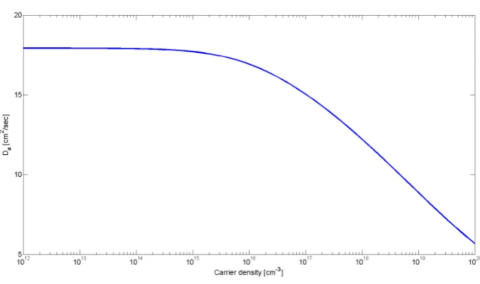
Carriers in silicon interact with the optical mode and induce loss and phase changes. Among the recombination processes described above, carriers that were generated locally by TPA will also diuse to low carrier density areas. Therefore, the interaction time of the mode with these carriers will be limited to the length of time they spend in the vicinity of the mode. It is therefore important to add diusion to our model. The diusion equation governing this process is given by:
dn
dt =D∇
2n (3.18)
whereD is the diusion coecient for silicon. For high carrier-densities we will have
to use the ambipolar diusion coecient given by [87]:
Da =
2KT q 1 µe + 1 µp −1 (3.19)
whereµe,pis the mobility of electrons/holes. When the carrier density is high,
carrier-carrier scattering will increase. This will reduce the mobility of the carrier-carriers further at high densities. I will model the eect of carrier density on mobility using [39]:
1
µe,p
= 1
µ(0)e,p
+∆ne,p·ln(1 + 4.54·10
11∆n−0.667
e,p )
1.428·1020 (3.20)
where ∆ne,p is electron/hole density in [cm
−3
] and the low-density mobility is taken to be:
µ0e = 1430 cm
2
V·sec (3.21)
µ0p = 495 cm
2
V·sec (3.22)
Figure 3.4: Model for the ambipolar diusion coecient of silicon
3.2.5 Eective carrier lifetime
The optical mode is conned within the three-dimensional cavity. In the longitudinal direction, the mode is designed to be a Gaussian with half-width in the order of hundreds of microns. In the transverse direction, the mode is conned to only a few microns. The orders of magnitude change in connement between longitudinal and transverse direction motivates us to approximate the longitudinal direction as having a uniform photon distribution. The gradient in carrier density in the longitudinal direction is much weaker than that of the transverse. Therefore, diusion in the longitudinal direction could be neglected. For the thin Si slab I can assume a uniform carrier density since the diusion length is much larger than that thickness (y direction in Figure 3.3). For that reason, I can approximate the whole problem using a 1-D diusion equation in the x direction only.
The generation-recombination-diusion equation describing the dynamic of the carriers in Si can be expressed as [16] :
dnSi
dt =
βThνΓ2SiVg2
2 n
2
p−
nSi
τb
−2S
HnSi+Da d2n
Si
dx2 (3.23)
rep-Figure 3.5: Carrier density prole for several dierent surface recombination proles
resents bulk recombination; the third term represents surface recombination, and the last term represents diusion. To gain more insight into the typical carrier distribu-tion I will assume that the generadistribu-tion of carriers is due to TPA induced by an optical mode with a Gaussian spatial prole:
np =
np,0
√ 2πe
−x2
2σ2 (3.24)
where the width of the Gaussian is chosen to be equal to the waveguide ridge width
σ = 2µm (see Figure 3.3). np,0 would be the average photon density, if the mode were
uniform within the waist area (np,0 = σ1
R
np(x)dx).
A numerical solution to Equation 3.23 is shown in Figure 3.5. A few conclusions can be drawn from this gure:
• Even for very fast surface recombination, the carrier prole is much broader than the mode's prole. This will motivate us to approximate the carrier density as uniform in the vicinity of the mode.
• Surface recombination is the main mechanism of recombination. Mode prole depends almost solely on the surface recombination velocity.
Figure 3.6: Eective lifetime of carrier in silicon for S=1cm sec
recombination velocity. However, as the surface recombination velocity becomes slower and slower the carrier-density peak eventually saturates.
Once I have numerically solved this equation for a given photon density prole, I can dene an eective lifetime for carriers in Si for the given optical mode:
τef f =
2
βThνv2gn2p
R
nSi(x)np(x)dx
R
np(x)dx
(3.25)
The parameterτef f represents the average time in which generated electrons interact
with the optical mode before they recombine at the surface or the bulk, or diuse away from the mode's area. A similar approach was taken by [16]. The eect of surface recombination velocity on this time constant is shown in Figure 3.6. We can identify three regimes in this gure:
1. Low carrier densities - The eective lifetime is constant for a wide range of rather low densities. This corresponds to the at area in the diusion coecient of Figure 3.4.