n
I
TMIOO-l, TMIOO-2
I
FLEXIBLE DISK DRIVES
I
P/N 179024-001
Notice 1
June 15, 1982
OEM OPERATING AND SERVICE MANuAL
TM100-3, -3M, -4, AND -4M DISK DRIVES
96/100 TRACKS PER INCH
TO ALL HOLDERS OF P/N 179024-001:
1.
Page
2-13,
Sections 2.6 through 2.6.1.11, has been revised
and
supersedes the one in the manual.
2.
Page 2-14,
Sections 2.6.2
through 2.6.2.7, has been added to the
manual.
3.
Retain this notice and
insert it
before
the table
of contents.
4.
Holders
of
P/N
179024-001 are requested to verifY that the page
changes and
additions
indicated
herein
have
been
entered.
This issuance is a
separate pUblication.
Each notice
is
to
be
retained until the
OEM
operat~ngand service manual is completely
revised.
Preparing Group:
TMIOO-l, TMIOO-2
5-l/4-INCH FLEXIBLE DISK DRIVES
48 TRACKS PER INCH
PRODUCT SPECIFICATION AND USER'S MANUAL
, an
Cliiil
CORPORATION20320 PRAIRIE STREET CHATSWORTH, CALIFORNIA 91311
Section Number
SECTION 1
Title
GENERAL DESCRIPTION
CONTENTS
Page Number
1.1
1.2 1.3
1.4
1.5
SECTION 2
2.1
2.2
2.3 2.4
SECTION 3
3.1
3.2
3.3
3.4
3.5 3.6
3.7
Introduction. . . 1-1
Scope Of The Document... 1-1
Purpose Of The Drive . . . 1-1
Major Features... 1-1
Write Protect. . . .. . . .. . .. . . 1-1
Daisy Chain Capability... 1-1
Internal Trim Erase... 1-1
Industry Standard Interface Compatibility... 1-1
Track
a
Switch... 1-2Index Sensor . . . 1-2 Activity Indicator. . . .. . . .. . . .. . . 1-2 Fwictional Description. . . .. . . .. . . .. . . .. . . 1-2
Physical Description 1-2
PRODUCT SPECIFICATIONS
Introduction .'. . . 2-1
Mechanical Specifications . . . 2-1
Electrical and Operational Specifications . . . 2-1
Reliability Specifications... .. 2-1
Environmental Specifications 2-1
OPERATION
Introduction. . . 3-1 Unpacking The Drive. . . 3-1
Preinstallation Checkout 3-1
Mounting The Drive ~... 3-1
Dust Cover . . . 3-2
Cooling : ;... 3-2
Interface Connections 3-2
Input Control Lines 3-2
Output Control Lines. . . 3-4 Typical Interface Characteristics. . . 3-4 D. C. Power. . . 3-5 Drive Address and Option Patching. . . 3-5 DSaThrough DS3 Jumpers. . . 3-5 MX Jumper . . . 3-7
HS and HM Jumpers 3-7
Power Save Option ~. . . 3-7
Side Select (WI) 3-7
Write Flip-Flop Control (W2, W3) 3-7
Write Protect Control (W4, W5) 3-7
Activity L.E.D. Control (W6, W7, W9) 3-7
Drive Select 3 Enable (W8) . . . 3-9
Door Lock Solenoid (WID) 3-9
Diskettes. . . .. .. . . .. . . .. . . . .. . . .. . . .. 3-9
Loading The Diskette 3-9
Write Protect Tab... 3-9
ILLUSTRATIONS
FIGURES
Figure Number
1-1 2-1 3-1
3-2
3-3
3-4 3-5 3-6
Title
Disk Drive .
Disk Drive Outline Drawing .
Electrical Interface Characteristics .
Control and Data Timing Requirements .
Logic Board With Programmable Shunts and Option Patching Locations .
Recording Media .
Write Protect Tab .
Diskette Handling and Storage .
TABLES
Page Number
1-3 2-2
3-5 3-6 3-8 3-10 3-11 3-12
Table Number
2-1
2-2 2-3
3-1
3-2
Page
Title Number
Electrical and Operational Specifications. . . 2-3
Reliability Specifications... 2-4
Environmental Specifications 2-5
Drive Interface Lines and Pin Assignments. . . 3-2
D. C. Power Connector Pin Assignments 3-5
SECTION 1
GENERAL DESCRIPTION
INTRODUCTION
This document provides required information in order to evaluate and incorporate Tandon'l:? disk drive into a system.
Tandon Corporation's Model Number TMI00-l and TMI00-2 are full-feature, 5-1/4-inch, flexi-ble disk drives. They are 'compact data storage devices that use an ANSI-compatible, industry standard, 5-1/4-inch diskette.
Model Number TMIOO-l and TMIOO-2 drives each have forty-eight (48) tracks per inch. The
TMI00-l is a single-sid~d recording deyice. The
TMI00-2 is a double-'sided recording device.
Both drives are capable of reading and writing in single-density format on a diskette, using a
proprietary read/write head patented by
Tandon. The drives have a double density capa-bility when Modified Frequency Modulation (MFM) or other appropriate recording technique is used. Encoding and decoding of the data is done by the user's controller.
1.1
SCOPE OF THE
DOCUMENT
This document contains the major features, physical and functional specifications, mounting and power requirements, the interface, and typi-cal timing characteristics of the TM100-1 and TMIOO-2 drives.
1.2
PURPOSE OF THE DRIVE
The TMI00-l and TMI00-2 drives are rotating disk memories designed for random access data
entry, storage, and retrieval applications.
Typical applications include intelligent terminal controllers, microcomputers, word processing systems, data communication systems, error
logging, program loading, and point-of-sale
terminals.
1.3
MAJOR FEATURES
WRITE PROTECT
When a write protected diskette is inserted into the drive, the write electronics are disabled.
DAISY CHAIN CAPABILITY
The drive provides the address selection and gating functions necessary to daisy chain a maximum of four units at the user's option. The last drive on the daisy chain terminates the interface. The terminations are accomplished by a resistor array plugged into a DIP socket.
INTERNAL TRIM ERASE
The drive provides the control signals necessary for proper trim erasure of data.
INDUSTRY STANDARD INTERFACE COMPATIBILITY
TRACK 0 SWITCH
The Track 0 switch is provided to generate a logic level at the drive interface, indicating the read/write head is positioned at the outermost track.
INDEX SENSOR
An index sensor is provided to generate
electrical pulses at the drive interface
coincident with sensing Index/Sector holes on the diskette.
ACTIVITY INDICATOR
An activity indicator, located on the front panel, is automatically illuminated when the drive is selected.
1.4
FUNCTIONAL DESCRIPTION
The drives are fully self-contained, and require
no operator intervention during normal
operation. Each drive consists of electronics to generate and interpret control signals, a head positioning system, a read/write system, and a spindle dri ve system.
When the front latch is opened, access is provid~dfor insertion of a diskette. The diskette is held in place by plastic guide rails. Its location is ensured when the diskette is inserted until a back stop is encountered.
Closing the front latch activates the cone
clamping mechanism, resulting in accurate centering and clamping of the diskette. The drive hub is held at a constant speed of 300 RPM by a servo-controlled D. C. motor. The heads remain in contact with the recording media until the front latch is opened.
The heads are positioned over the desired track by means of a four-phase stepper motor/band
1-2
assembly and its associated electronics. This positioner uses a one-step rotation to cause a one track linear movement.
Data recovery electronics include a low-level read amplifier, differentiator, zero crossover
detector, and digitizing circuits. No data
decoding capabilities are provided.
The drive has the following sensors:
1. A Track 0 switch detects when the
head/carriage assembly is positioned at Track
o.
2. An index/sensor is positioned to generate
a digital signal when an index/sensor hole on the diskette is detected.
3. A write protect switch disables the write
electronics when a write protect tab is applied to the diskette.
1.5
PHYSICAL DESCRIPTION
A representative drive is shown in Figure I-I. The drive can be mounted in a vertical or horizontal plane. However, the logic circuit board must be on the uppermost side when the drive is mounted horizontally.
The spindle is belt' driven by a D. C. motor with
an integral tachometer. The servo control
circuit and tachometer control the speed of the spindle.
The read/write head assembly is positioned by a split band positioner mounted to a stepper motor. The read/write head(s) is a glass-bonded, ferrite/ceramic 'structure with a life expectancy of 20,000 operating hours.
FRONT PANEL
FRONT LATCH
ACTIVITY INDICATOR
LOGIC CIRCUIT BOARD
CONE ASSEMBLY
FIGURE1-1
DISK DRIVE
D.C. DRIVE MOTOR
READ/WRITE HEAD ASSEMBLY
RESISTOR ARRAY
STEPPER MOTOR
DRIVE CHASSIS
SECTION 2
PRODUCT SPECIFICATIONS
INTRODUCTION
This section contains the mechanical, electrical reliability, and environmental specifications for the TM100-1 and TMIOO-2 drives.
2.1
MECHANICAL SPECIFICATIONS
The physical dimensions of the dri ve are located in Figure 2-1.
2.2
ELECTR,JCAL AND OPERATIONAL SPECIFICATIONS
The electrical and operational specifications are located in Table 2-1.
2.3
RELIABILITY SPECIFICATIONS
The reliability specifications are located in Table 2-2.
2.4
ENVIRONMENTAL SPECIFICATIONS
The environmental specifications are located in Table 2-3.
, a n
a
D
n
CORPORATION, CHATSWORTH. CALIFORNIA 913112-1
179059-001
086 121 B4 MMI
187 14750MMI
:$12 17925 MM)
r
Il--+---f-0.06 (152 MM) SERVO
CIRCUIT
BOARD
I
1
0.13 1330MM)
06 1152MM)
1203 8
2
0 0 0
MM)
r-7.751119685MM)
I
I
17932~~M)I
i
t--.~~~~
I I 1 87
I I 14750MMI
1
1
t1
019
JI
5871483MMI 1~(----114910MMI 029
1737 MMI
_
.._--_._--j-338 18585 MMI
NOTES: 1. DIMENSIONS ARE GIVEN IN INCHES. METRIC EQUIVALENTS ARE IN PARENTHESES.
2. TOLERANCE ON ALL DIMENSIONS ±0.020 INCH, UNLESS OTHERWISE SPECIFIED.
3. WEIGHT IS APPROXIMATELY 3 POUNDS (1.35 KILOGRAMS).
FIGURE 2-1
DISK DRIVE OUTLINE DRAWING
'anCion
CORPORATION, CHATSWORTH, CALIFORNIA 91311179059-001
Media
TABLE 2-1
ELECTRICAL AND OPERATIONAL SPECIFICATIONS
ANSI-compatible, 5-1/4-inch diskette
Media Life (for reference only)
Tracks Per Inch
Tracks Per Drive
TMIOO-l
TMIOO-2
Track Spacing
Head Life
Disk Rotational Speed
Averag~Rotational Latency
Instantaneous Speed Variation (ISV)
Motor Start Time
Motor Stop Time
Seek Time, track-to-track
Head Settling Time
Average Track Access Time, including head settling time
Typical Recording Modes
Data Transfer Rate
Flux Reversals Per Inch (FRPD, inside track
Both Models, Side 0
TMIOO-2, Side 1
6
4 x 10 passes per track
48 TPI, both drives
40 tracks
80 tracks
0.529 millimeters, 20.8 milinches
20,000 media contact hours
300 RPM± 1.5 percent
100 milliseconds
± 3 percent
250 milliseconds, maximum
150 milliseconds, maximum
5 milliseconds
15 milliseconds
75 milliseconds
FM, MFM, MMFM
250,000 bits per second, double density
5,535 FRPI
5,877 FRPI
'andon
CORPORATION, CHATSWORTH, CALIFORNIA 913112-3
TABLE 2-1 (CONTINUED)
ELECTRICAL AND OPERATIONAL SPECIFICATIONS
Unformatted Recording Capacity
TM100-1
TM100-2
D. C. Voltage and Current Requirements
+
12 volts D. C. Power+5 volts D. C. Power
Shipment
250 kilobytes per disk
500 kilobytes per disk
+
12 volts ± 0.6 volt, 900 milliamperes, average, 100 milli volts peak-to-peak ripple.i~.5 volts'± 0.25 volt, 600 milliamperes, average, with less than 100 millivolts peak-to-peak ripple.
When prepared for shipment by Tandon, the drive meets the requirements of NSTA preshipment test procedure Project lA.
TABLE 2-2
RELIABILITY SPECIFICATIONS
Error Rates, maximum, exclusive of external sources, e.g.: electronics, defective and contaminated diskettes
Soft Errors (Recoverable)
Hard Errors (Nonrecoverable)
Seek Errors
Mean Time Between Failures
Mean Time To Repair
One in 109bits
One in 1012bits
One in 106seeks
8,000 hours, 25 percent duty cycle
30 minutes
, a n
a []
n
CORPORATION, CHATSWORTH, CALIFORNIA 91311179059-001
TABLE 2-3
ENVIRONMENTAL SPECIFICATIONS
Temperature
Operating, media dependent
Nonoperating
Relative Humidity
Operating, noncondensing, media dependent
Nonoperating, noncolldensing
Altitude
Operating or nonoperating
10°C to 46°C, 50°F to 115°F
-40°C to 71 °c, -40°F to 160°F
20-to-80 percent
5-to-95 percent
152.4 meters, 500 feet, below sea level, to 15,240 meters, 50,000 feet, above sea level
, a n
aD
n
CORPORATION, CHATSWORTH, CALIFORNIA 913112-5
179059-001
2.6
96/100 TPI
TRACK 00 SENSOR CHECK AND ADJUSTMENT
The Track 00 sensor provides a signal that identifies Track 00 to the
logic electronics. The logic electronics disable the step-out
function when Track 00 is reached. In addition, a Track 00 signal is
sent to the controller on Pin 26 of the interface.
2.6.1.
2.6.1.1
2.6.1.2
2.6.1.4
2.6.1.6
2.6.1.7
2.6.1.8
2.6.1.11
2.6.1.12
2.6.1.13
2.6.1.14
Track 00 Sensor Check
Set up a dual-channel, wideband oscilloscope as follows:
Channel A, Test Point 1; Channel B, Test Point 2
Ground: Test Point 10
Read Differentially: A plus B, B inverted
Time Base: 20 milliseconds per division
External Trigger: T~st Point 7, positive edge
Vertical Display: 0.1 volt per division
Apply power to the drive'.
Insert a Cats Eye alignment diskette into the drive.
Close the front door.
Step the carriage to the radial alignment track.
·0
Confirm the position by observing the' Cats Eye pattern.
Set up the oscilloscope to monitor the TTL signal at IC4B,
Pin
9,
or at P11, Pin 2.Step the carriage back to Track 01.
Ensure that the signal at Track 01 is at least 2.5 volts.
Step the carriage out to the radial alignment track.
Step the carriage back to Track 02.
Verify that the logic level at IC4B, Pin 9, is less than
0.8 volt.
If all of the above checks are satisfactory, no adjustment
is required.
If one of the above checks is unsatisfactory, perform the
2.6.2
2.6.2.1
2.6.2.2
2.6.2.3
96/100 TPI
Track 00 Sensor Adjustment Procedure
Loosen
the
retaining
screw
on
the base of the Track 00
bracket.
Retighten
the
retaining
screw
slightly
to provide some
friction on the bracket.
Rotate
the
Track 00 adjustment screw,
located at the rear
of
the
chassis,
counterclockwise
as
far
as it will go
without forcing it.
2.6.2.4
Step
the
alignment
Track 00.
carriage
back
track,
taking
to
Track
care
not
01
from
the
radial
to restore it back to
2.6.2.5
2.6.2.6
2.6.2.7
Rotate
the
Track
00
adjustment
screw
clockwise,
very
slowly,
until
the
signal at IC4B,
Pin 9,
is at least 2.5
volts at Track 01 and less than 0.8 volt at Track 02.
Retighten the retaining ?crew.
\:..Repeat
Steps
2.6.1.5
through 2.6.1.14 to ensure that the
SECTION 3
OPERATION
INTRODUCTION
3. Remove the cardboard shipping insert,and retain for future shipment.
This section contains information on how to unpack, check out, install, and operate the
TMIOO-landTMIOO-2drives.
1
I
"
3.1
UNPACKING THE DRIVE
4. Ensure the front panel is secure.
5. Ensure the drive belt is in place.
6. Manually rotate the drive hub. Itshould
rotate freely.
7. Ensure both circuit boards are secure.
The drives are packaged in protective containers to minimize the possibility of damage during shipment. The following list is the recommended procedure for unpacking the drive.
1. Place the container on a flat work
surface.
2. Remove the upper half of the container.
3. Remove the drive from the lower half of
the container.
4. Check the contents of the container
against the packing slip.
5. Investigate the contents of the container
for possible damage.
6. Notify the carrier immediately if any
damage is found.
3.2
PREINSTALLATION
CHECKOUT
Before applying power to the drive, the following inspection should be conducted:
1. Check to ensure the front latch opens
and closes.
2. When the latch is moved to an open
posi-tion' the head arm raises.
3-1
8. Ensure the connectors are firmly seated.
3.3
MOUNTING THE DRIVE
The drive has been designed to be mounted hori-zontally or vertically. When mounted horizon-tally, the logic circuit board side of the drive must be the top side.
Four 6-32 tapped mounting holes are provided on the bottom of the drive, and two 6-32 tapped mounting holes on each side, for attachment to
user-supplied mounting brackets. When
in-stalled in either plane, horizontal or vertical, only.two mounting screws are required to secure-ly hold the drive in place.
Any mounting scheme in which the drive is part of the structural integrity of the enclosure is not permitted. Mounting schemes should allow for adjustable brackets or incorporate resilient
members to accommodate tolerances. In
addi-tion, it is recommended that mounting schemes include no more than two mounting surfaces.
The drive is manufactured and tested with some
critical internal alignments that must be
DUST COVER
The design of an enclosure should incorporate a means to prevent contamination from loose items, e.g., dust, lint, and paper chad, since the drive does not have a dust cover.
COOLING
Heat dissipation from a single drive is normally 15 watts, 51 BTU per hour, under high load con-ditions. When the drive is mounted so the compo-nents have access to a free flow of air, normal convection cooling allows operation wi thin the specified temperature range.
When the drive is mounted in a confined envi-ronment, air flow must be provided to maintain specified air temperatures in the vicinity of the motors, printed circuit board, and diskettes.
When forced air is used, air flow must be direct-ed outward from the drive. Do not intake air through the drive or heads and diskettes.
3.4
INTERFACE CONNECTIONS
Interface connections for the TMI00-l and TMI00-2 are made via a user-supplied, thirty-four pin, flat ribbon connector, 3M Part Number 3463-0001 or Amp Part Number 583717-5, using contact Part Number 1-583616-1 for twisted pair or its equivalent. This connector mates directly with the circuit board connector at the rear of the drive. The D. C. power connector is a four-pin connector at the rear of the drive. The interface description of the connectors, and the location of each one, is contained in this section. Interface lines are located in Table 3-1. D. C. power connector pin assignments are located in Table 3-2.
The signal wire harness should be of the flat ribbon or twisted pair type, 26-to-28 gauge conductor, compatible with the connector to be used. The recommended cable length is ten feet maximum.
3-2
TABLE 3-1
DRIVE INTERFACE LINES AND PIN ASSIGNMENTS
Input Control Lines: Controller-To-Disk Drive
Ground Pin Signal
1 2 Connector Clamp
3 4 Spare
5 6 Drive Select 3
9 10 Drive Select 0
11 12 Drive Select 1
13 14 Drive Select 2
15 16 MotorOn
17 18 Direction Select
19 20 Step
21 22 Composite Write Data
23 24 Write Enable
31 32 Side Select
Output Control Lines: Disk Drive-To-Controller
Ground Pin Signal
7 8 Index/Sector
25 26 Track 0
27 28 Write Protect
29 30 Composite Read Data
33 34 Spare
INPUT CONTROL LINES
DRIVE SELECT LINES
The Drive Select lines provide a means of select-ing and deselectselect-ing a drive. These four lines select one of the four drives attached to the controller.
Read/Write command is completed. When the signal line logic level is false (high), the input control lines and output status lines are disabled.
The drive address is determined by a j urnper select on the logic circuit board. Drive Select lines 0 through 3 provide a means of daisy chain-ing a maximum of four drives to a controller. Only one can be true (low) at a time. An unde-fined operation results if two or more drives are assigned the same address or if two or more Drive Select lines are in the true (low) state simultaneously.
MOTOR ON
When this signal is true (low), the drive motor accelerates to its nominal speed of 300 RPM, and stabilizes at this speed in less than 250 milliseconds. When the signal line logic level goes false (high), the drive decelerates to a stop. This signal is not gated with Drive Select.
The motor activates momentarily when the front latch is closed. This motor start function remains active for approximately five seconds, unless Motor On is in the true (low) condition.
DIRECTION SELECT AND STEP LINES (TWO LINES)
When the drive is selected, a true Clow) pulse on the Step line, with a time duration greater than 200 nanoseconds, initiates the access motion. The direction of motion is determined by the logic state of the Direction Select line when a step pulse is issued. The motion is toward the center of the disk if the Direction Select line is in the true (low) state. The direction of motion is away from the center of the disk if the Direction Select line is in the false (high) state.
To ensure proper positioning, the Direction Select line should be stable at least 100 nanosec-onds prior to issuing a corresponding step pulse, and remain true (low) 100 nanoseconds after it.
The access motion is initiated on the trailing edge of the step pulse. The time period between consecutive trailing edges of step pulses should be not less than five milliseconds.
3-3
The drive electronics ignore step pulses when one of three conditions exists:
1. The write enable is true (low).
2. The direction select is false (high), and
the head is positioned at TrackO.
3. The drive is not selected.
COMPOSITE WRITE DATA
When the drive is selected, this interface line provides the bit serial composite write data pulses that control the switching of the write current in the selected head. The write elec-tronics must be conditioned for writing by the Write Enable line.
For each high-to-low transition on the Composite Write Data line, a flux change is produced at the write head gap. This causes a flux change to be recorded on the media.
When a single-density (FM) type encoding tech-nique is used in which data and clock form the combined Write Data signal, it is recommended that the repetition of the high-to-low transi-tions, while writing all zeros, be equal to one-half
the maximum data rate, 125 kilohertz ± 0.1
percent, and the repetition of the high-to-Iow transitions, when writing all ones, be equal to
the maximum data rate, 250 kilohertz ± 0.1
percent.
Host controllers may implement write precom-pensation circuits that recognize worst case pat-terns and adjust the write data waveform.
, Although a value cannot be specified for writ~
precompensation, Tandon suggests a value of 250 nanoseconds for systems using MFM double density recording format.
WRITE ENABLE
When this signal is true (low), the write
electronics are prepared for writing data and the read electronics are disabled. This signal turns on write current in the selected read/write head. Data is written under the control of the Composite Write Data and Side Select input lines. When the Write Enable line is false
When a write protected diskette is installed in a drive, the write electronics are disabled, irre-spective of the state of the Write Enable or Side Select lines.
SIDE SELECT, TM100-2
The Side Select interface line defines which side of a two-sided diskette is used for data transfer.
A false Chigh) level on this line selects the read/write head on side zero, the lower head, of the drive. A true (low) level on this line selects the read/write head on side one, the upper head of the drive.
OUTPUT CONTROL LINES
INDEX/SECTOR
The index/sector signal is a composite of the index pulse and sector signals.
An index pulse is provided once every revol
u-tion, 200 milliseconds nominal, to indicate the beginning of a track to the controller. The lead-ing edge of this signal must al ways be used to ensure timing accuracy. The index/sector line re-mains in the true (low) state for the duration of
the index pulse, which is nominally four
milliseconds.
WRITE PROTECT
When the Write Protect line goes true (low), the
diskette is write protected and the write
electronics are disabled. It is recommended the
controller not issue a Write command when the Write Protect signal is true (low).
When the Write Protect line is false (high), the write electronics can be enabled.
COMPOSITE READ DATA
This interface line transmits the readback data to the controller when the drive is selected.
It provides a pulse for each flux transition
de-tected from the diskette. The Composite Read Data output line goes true (low) for a duration
of 1 ± 0.25 microseconds for each flux change
detected from the diskette.
The leading edge of the Composite Read Data output pulse represents the true position of the flux transitions on the diskette's surface.
TYPICAL INTERFACE CHARACTERISTICS
Lines between the controller and the drive have the following characteristics:
VoutTrue =
+
0.4 volt maximum atlout=:= 48 milliamperes, maximum
Figure 3-1 contains the characteristics of the electrical interface. Figure 3-2 contains the con-trol and data timing requirements.
The sector signal portion appears only when using hard sectored diskettes.
TRACK 0
When the drive is selected, the Track 0 interface signal, when true (low), indicates to the control-ler that the read/write head (s) are positioned at Track O. This signal remains true (low) until the heads are moved from Track O.
3-4
VoutFalse
+
2.4 volts minim urn opencollector atlout = 250
I I
r-- - - - l I
I I I
+TRUE _~I
---1[>0
x
I:
:
J :
I: 74380R I I
L
EQ~VALENT
_ _J :
I
DRIVER I I
+5 VOLTS
150 OHMS
74LS04 OR EQUIVALENT
~
<:{>--+TRUETRANSMISSION I
LINE~10 FEET I
I
I
-=-I
I RECEIVER
I
FIGURE 3-1
ELECTRICAL INTERFACE CHARACTERISTICS
3.5
D. C. POWER
D. C. power is supplied to the drive via a four-pin AMP connector, J2, mounted on the circuit board. The mating connector, not supplied, is AMP Part Number 1-480424-0, using AMP con-tact Part Number 606191-1. Pin assignments are found in Table 3-2. The conductor should be 16-to-18 AWG, minimum.
TABLE 3-2
D. C. POWER CONNECTOR PIN ASSIGNMENTS
Pin Supply Voltage
1
+
12 volts D. C.2 12 volts return
3 5 volts return
4
+
5 volts D. C.Pin Signal
Ground lug 3/16-inch Chassis ground from
quick disconnect controller
3-5
The chassis should be connected to earth ground
to ensure proper operation. The conduct,or
should be 16-to-18 AWG, minimum.
3.6
DRIVE ADDRESS AND
OPTION PATCHING
The drive address and option patching is
deter-mined by the programmable shunt located at IE
on the logic circuit board. The DSO through DS3 jumpers determine the drive address. The MX jumper is used only in single drive systems. See Figure 3-3.
The program shunt is AMP Part Number 435704-7. The shunt positions can be cut using AMP's tool, Part Number 435705. The shunt is installed in a DIP socket. At the user's option, it can be removed and replaced by a DIP switch.
DSO THROUGH DS3 JUMPERS
POWER ON
I - - - .
Sl~---,
t--
100 MILLISECONDSI
MINIMUM- - - - I
DRIVE SELECT---~I)oS
-MOTOR ON
~---____l,~ ~s
-500 NANOSECONDS--..../
MAXIMUM
I
250 MILLISECONDS---...j
MAXIMUM
I
i
200MILLISECONDS±31
INDEX
---,U
U,...--~Ss S---l
1--4 MILLISECONDS'r-TRACK 0
---,~'---\S ~~---
500 NANOSECONDS--...l
MAXIMUM I
WRITE PROTECT
IL..---ss
~f
-DIRECTION
SIDE SELECT
~---ff
J
_--I 100 NANOSECONDS
1-~ MINIMUM ~
I
'---4'
~f_ _- - - l5 MILLISECONDS--...j ~ 100
MINIMUM NANOSECONDS
1
r-200 NANOSECONDS--.J 1__ MINIMUM
MINIMUM I
r--S T E P - - - j - - . , L J U S
LJr---100 NANOSECONDS,1-1
1---1
r
MINIMUM ~ ~ 20 MILLISECONDS
I MAXIMUM
I
WRITE ENABLE L..- 250 MILLISECONDS ~ I
I - MINIMUM -iIII'1 S~
I 900 MICROSECONDS"
--...i
r--390 MICROSECONDS"--1
r--
I
I
ERASE G A T E - - - . : . . . . ;- - - "
Ir----(TUNNEL ERASE) 200 NANOSECONDS llIIIIII ...1 ~s
MINIMUM
12100 NANOSECONDS
\..-.+-
4 MICROSECONDSIMAXIMUM
I
I
WRlnD~---1-0-0-M-I-C-R-O-S-E-C-O-N-D-S-~-.:....~-I-·---~~
MINIMUM I _I L
4 MICROSECONDS
r-
-.,
1
8 MICROSECONDSREAD DATA,.-·
- - - 1
LJLrLr
~
1 )-250 MILLISECONDS
I
J-
L
I I
1 MICROSECONDMINIMUM
-....t
--i
r--
± 250 NANOSECONDS8 MICROSECONDS
"FOR REFERENCE ONLY
FIGURE3·2
CONTROL AND DATA TIMING REQUIREMENTS
that addresses each individual drive in the daisy
chain. The terminator resistor pack, RPl,
located on the logic circuit board should be in-stalled in the last drive of the daisy chain. All other drives on the interface must have the resistor pack removed.
WRITE FLIP-FLOP CONTROL (W2, W3)
W2 and W3 control the set and preset lines of the write flip-flop, IC-5C. W2 is installed for the standard configuration, W3 is for special use.
MX JUMPER
The Multiplex (MX) jumper is used only in single drive systems when the user requires the drive logics to be enabled at all times. If the drive is not selected through the DS jumper, and the MX jumper is not cut, the drive logics are enabled but the front panel L.E.D. is not on. The MX jumper must be cut in a multiple drive system.
...
.
W2
x
W3
x
WRITE FLIP-FLOP CONTROL
Disables set and preset lines on the write flip-flop only during internal N Write. Disables set and preset lines on the write flip-flop
continuously.
HS AND HM JUMPERS
HS and HM j umpers are not used, and must be cut.
WRITE PROTECT CONTROL (W4, W5)
Write Protect Control from the write protect switch is disabled with W5 installed. Standard Write Protect Control is enabled with W4 installed.
ACTIVITY L.E.D. CONTROL (W6, W7, W9)
The Activity L.E.D. may be illuminated by an optional input line, Jl-4 CN In Use). Normally, the Activity L.E.D. is controlled with Drive Select, W6 installed.
POWER SAVE OPTION
When shipped from the factory, the drive is con-figured with a jumper at R51, 0 ohm resistor, for the TMIOO-l and TMI00-2 drives. R51 main-tains 200 milliamperes of current to the stepper motor whether or not the drive is selected. Main-taining power to this motor prevents the head carriage from moving when the drive is not selected. The jumper at R51 may be moved to position R50, which removes the power to the stepper motor when the drive is not sele.cted, for a savings of approximately 3.8 watts per drive. When R50 is used, the user must ensure the track location when the drive is reselected.
SIDE SELECT (W1)
For use in double-sided drives:
W4
x
W6
W5
x
W7
WRITE PROTECT CONTROL
Write Protect Control
responds to a write protected diskette.
Write Protect Control is inhibited.
W9 ACTIVITY L. E. D. CONTROL
WI
x
SIDE SELECT
For use in single-sided drives, TMIOO-l.
For use in double-sided drives, TMIOO-2.
3-7
x
x
x
Activity L.E.D. is controlled with Drive Select.
DRIVE SELECT 3 ENABLE (W8)
Removal of this jumper allows interface Jl-6 to be used as an alternate input/output line. W8 is normally installed.
W8 DRIVE SELECT 3 ENABLE
X Allows drive to be selected via Jl-6.
Disables Drive Select 3 line.
DOOR LOCK SOLENOID (W10)
This jumper is used in conjunction with an optional door lock solenoid. The WIO jumper is normally not installed.
WIO DOOR LOCK SOLENOID
X Enables door lock solenoid via Jl-2.
Disables door lock circui ts.
3.7
DISKETTES
The TM100-1 and TM100- 2 drives use an
ANSI-compatible, 5-l/4-inch diskette. Diskettes are available with a single index hole or with multiple (index and sector) holes.
Diskettes with a single hole are used when soft
sector format is required. Multiple hole
diskettes provide sector information through the use of an index sensor and electronics.
Figure 3-4 illustrates the diskette used with the
drive. This recording media is a flexible diskette enclosed in a protective jacket. The protected diskette, free to rotate within the jacket, is continuously cleaned by its soft fabric lining during normal operation.
LOADING THE DISKETTE
The drive is loaded by inserting the diskette, head aperture forward, into the front slot of the drive. Access to the diskette loading slot is obtained by opening the front latch.
The diskette should be carefully inserted until it is solidly against the back stop.
3-9
CAUTION
Damage to the center of the
diskette may result if the door is closed when the diskette is not
properly inserted. This prevents
reliable recovery of the recorded data.
WRITE PROTECT TAB
The drive is equipped with a write protect
switch assembly. This switch operates in
conjunction with a diskette that has a slot cut in the protective jacket. Figure 3-5 contains the location of the slot.
When the slot is covered with an optically opaque, self-adhesive tab, the diskette is write
protected. The tab illust be removed to write on
the diskette. Figure 3-5 contains information on how to install a tab to cover the slot.
DISKETTE HANDLING AND STORAGE
It is important the diskette be handled and
stored correctly so the integrity of the recorded data is maintained. A damaged or contaminated diskette can impair or prevent recovery of data, and can result in damage to the read/write head(s).
Figure 3-5 contains an illustration of the
physical configuration of the diskette. The
5.125-inch diskette is oxide-coated, flexible
mylar. It is enclosed in a 5-1/4-inch square
protective jacket. Read/write head access is made through an aperture in the jacket. In addi-tion, openings for the drive hub and diskette index hole are provided.
Figure 3-6 provides some helpful hints on the care and handling of the drive and diskettes. In addition, to ensure trouble-free operation and to enhance the service life of the diskette, the
following handling procedures should be
observed.
1. Return the diskette to the protective
jacket when not in use.
2. Avoid exposing the diskette to any
o
o
W5000W4
,..---,
~_'2_~9J
R51 oCJo °R500 W20
00W3
W7
00 W6
00
TERMINATOR SOCKET (2F) PROGRAMMABLE
SHUNT SOCKET (1
E)-+--.-LOGIC CIRCUIT BOARD
HS NOT USED' 16
2 DSO 15
3 DS1 14
4 DS2 13
5 DS3 12
6 MX 11
7 SPARE 10
8 HM NOT USED 9
PROGRAMMABLESHUNTSOCKET1E
FIGURE3-3
NOTE
The 50-oersted level magnetizing force is reached at a distance of approximately three inches from a typical source, e.g., motors, gen-erators, or transformers.
3. To avoid warping, do not store the
diskette in direct sunlight.
4. Do not use a lead pencil or a ballpoint
pen to write on the label. Use a felt tipped pen, and mark lightly on the label.
96.5 ± 0.25 MM (3.80:!:: 0.01 INCH)
133.4 MM (5.25 INCH)
3.56 MM (O.14INCH)
l
r
iI 6.30:±: 0.25 MM
l...---+---h"
I
J
10.25± 0.01 INCH)I
--r
133.4 MM (5.25 INCH)
L
L
SEALED PROTECTIVE JACKET
L1NER~
133.4 MM
r
15.25 INCH)1
SPINDLE ACCESS HOLE
HEAD APERTURE
FIGURE 3-4 RECORDING MEDIA
WRITE PROTECT TAB
' - WRITE PROTECT TAB
'L FOLD OVER BACK OF DISKETTE
3.56 MM
-l
r
(0.14 INCH)6.30 MM
r---+,r
J
(0.25 INCH)f
96.5 MM (3.808 INCHES)
INDEX ACCESS HOLE
FIGURE 3·5 WRITE PROTECT TAB
DO NOT WRITE ON THE JACKET WITH PEN OR PENCIL. USE A FELT TIPPED PEN.
DO NOT TOUCH PRECI-SION SURFACE WITH YOUR FINGERS.
TO AVOID DAMAGE TO THE DISKETTE AND TO YOUR DRIVE, INSERT DISKETTE CAREFULLY UNTIL THE BACKSTOP IS ENCOUNTERED.
RETURN THE DISKETTE TO ITS JACKET WHEN NOT IN USE.
KEEP THE DISKETTE
AWAY FROM
MAG-NETIC FIELDS.
DISKETTES SHOULD
BE STORED AT
10°Cto52°C
50°Fto125°F
HANDLE WITH CARE; BENDING AND
FOLD-ING MAY DAMAGE
DISKETTE.
FIGURE3-6
DISKETTE HANDLING AND STORAGE
A 4 7 \.987 7 /2. 8 14 \4
U.5ED ON ASM
OA cSc27-2.
1
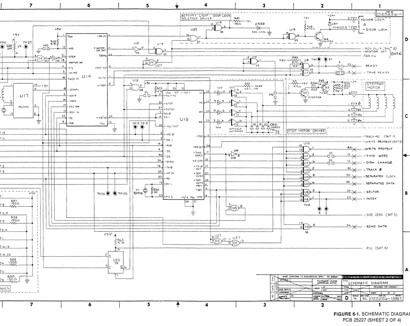
FIGURE 6·1. SCHEMATIC DIAGRAM,
PCB 25227 (SHEET 1 OF 4)
r-:-...:...:.-+--=--:..--+---l---'-t----l
0252"27;'- ,
t-.JOiES: UNLESS OTHERWISE' - - - i
SPECiFIED-I. ALLCAPACITORS ARE;N ~1!CRO::I~P.ADS
SOYI +8:)-20°0
2. ALLDiODES ARE IN4:4S
3. AL.L.. RESiSTORS ARE IN JHt-v1S 1/4\// 5°,:,; 0
1% RESISTORS ARE !/8W.
4.-0-0- INDICATES CUT-TRACE OPTION.
5.
-a
0-INDICATES SHORTiN6 PllJ6 OPTIO/,\ 6.~ :f..JDICA1ES SHORTING PLUG( FACTORY INSTALLED).
7.DISTRIBUTE 0.1 CAPACiTORS ON +5V
AND +24 V BUS LINES.
8.NPN TRAN3IS-:-0RS ARE PARTOl=CAj083
9.PNP TRANSISTJR5 ARE PAR.TOFIPQ~906.
IO.INDUCTORS APE .!10%.
2 2 TOUl'lANCE UM..ESS OTHERWIs.E NOTED +24'1 R28
MUST CONFORM TO ENGINeERING_c E S - . o
\3 3 3 IK 4 4 \1.0
7 U4 R~S R:S6
/ +b"<.,- - ' V IK\/\ro--<t-- "',v'S.\r-___,
\ "T v
,/
8'
IL ~ _
U4 CA3Q83 R\\.,RbO CRi?c 5 5 C ~4-CRc3 Q II f( '7C? TP 2"7
IREFERENCE DESIGNATIONS
LAST USED t-JOTUSED
R8
lOOt<
.----..--A..i"'V"'V--+24 Y
1- C36 v
~. 0.1
6
6
. CHASSIS GND
+?V
RI3 Rl4
S4,'?'?K<:'17.4 K
RI2. 1% 3 1%
_~.31K 2f?\U5
v v
\%
7
+e;,'1
- - - > . . 2 ; - - - + - + - - - t _ - - - . .
--->..'ijl--I---... .L4V
J0f1C39
T~O~
11PIO
1.
01_ _ _---->..2;--2_...-+=L2.o::;..o.:..;;yo"----'_--~~'-- 24 VR
_ _ _'ij-_3-+--.-=-:::-;::;--.-_ _
---ir--_
8 8
SIDE I CT
S 112 (12179)
I
1
Tt-f
c.'2.70
I ">, , - ->R' ('3 (2 Ref <<
1
. C81
.Lc.'14 CR \ -..;c--~ TP2. IW C 1.9I ;>150 0.1 0.1 4.7K
<
LI 0.1 .1 It--.!.",A2B ~ o.1_- 6 I
~" ~
~
~~3
IOO)lh "::'2?:>CS,Yo -... I'2V,S%~lh
SHiELD 0 ~
>-
..
n v 'Ie ...L- -..- ~ I';R2 ?R3 CI A c... )1
1
•
114 10 "::'Jb - ~ ")~v S22K - 022 ..,A,J C4 TPI ' - - ~
p/W ¢ I
r-- - -
-:-l CRI L I .. ..:" < - "''CRII -'~RI:2 RI3 . \OC~F 0.1 CS ~ Ul ?~'Z;-"2..2-~1---"31r-I>-r~/wo,,, 4 -:I~50YJO% R2.3'" ~OVt=.%
1550
PF I / I:
~
I " 3I
CR2I"J:
.,>R'3 -=-"'I 3 3'10~, ~
0~
I~o~
~'4 ~ j~,:~f ~.f
SIDE 0CT I ) I ,,~ $4.'67K .IC?4- 17 \.."2. 0./ < R2./ "::' 2.4K
~
I , " 2 CR3 I~
1'70T
~g~~~% ~U2
16 loO,uhc~
)~~4 ~~~S>
10K~~
9C20FJ ' ~ 4 RI7R20> 510~ Rl5
R/W yf2 d~
.
CRLl II lOOK:> 0 I K~J
I I Ic.
7 <R32~c.:
- - ' - - - ' V V ' v t~
>-n
r '"' 0 II
D.I )0 K R 18 L-ER ASE0 r 1'---- '-K. \ -I "::' ...----"'\I"v"\r--+---...
R/WII ~ 1~3 CRSI"I:
=-
'2.00 1'8,,
b:';
I [READ C.HAN~~~
I '" " 4 CR(o~
II 15 YBSr1-
.
HDIFFIN ~TPI6;
~
: , 5 CRrl I CIO 7~,FFIN
DATA 10I
::;:E I :
~ ~~}Cl
:
~;
~:
:--- - --- -- - --- -
---r---
---i
R2;24VISOP[~.V~;~:
U2
OUTr----+--+~~i~'A
I ~ , 6 C.RC1.1 I I I 2201' R2~ ell PS2 \6<:78-0 ,---I-.C-_.-.-T-p.-"-.S-L-E---,
L .-J " " VI I I 3WI%? 9.53K< ----i~OS 2 GND~ I - - -...---""""""""~~=_:_:=---r--_,______l
SHIEL\) \- - - ',>-r!-,
I
READ/W~\TE.II II
'/
VSw'I% 150 r 12 -L TYPE POSITIONI -J- CIt? +'?V J 50yP+,.-DIFFCOMP - ~:::'=:"':"~~~-+--+----j
' - - " : : ' M A-l"_1<-\t I I O. \
J
I I -=- (16if"'
1-5~9=-:2:-+_-::-____lf-- ~-+---::::----J- - - _::J ... _H RIO RCJ I POWER I IN52~'IB 1'-12 5% DIFFCOMP Ic'o278-0
~ ~ \0 ~oo 300 I R~~ET I 5.IV,5%_0.1 ~R27
m
vee Ic'o270-1s
Gt-JI) 3W 3W I I - ~2.15KI
II CA3C8~f
-WKITE DATA---<:lWRDATA ER~ 13 II
1/8W4 \4 24V 1%, "Clt::
(SI-lT3'l,-.WRITE GATE---qv-JR<;A-1ECT~-- 1-
L
L-~=+ --'\30.1
-h
- - , ~.:...j.:::.IDf:-r1l rD\ II 1 -- - - , 3/4'vV
1
1
... S\DE. rj; ~ r;;.'-f-I t::r-- +Z4-V I R 4 1 ' I [0%
~+I2St.L (\ \~
1
I CI4 1<4'2.. 7.IS\<' L - -r--J- Fl-,C)<e I .01 +S>V 4.1K 1°/
0 >
Rill
RClAr~
WRITE.I
ERA.'SE.d
VI-
T R.3~"::'v f VRE:FLJ3 \62.10-\YBB IS C~4'" Ie??1
22J\.V V V I r--il---<\0% R':l..:{-,., 12 --I-',-~--.---,S> US 10 IS()\%I
10KDRIVE.R
~
HEAD SElEC.T "::'~I
I7;~OK
'2 lRE'Fl~~V
rbl,r
I -l ...~
13 US Co US .,,-iH-'J"--..---...10% i<./wtRh.J 20% I 14 R40 7TPQ390b
8'
\
\'2. ~ 7 -=- -=- I ~~(.,"::' "Z..3ZK - >1<.4'3 \
'-f' \"10 >\0.1K.
I ~ RI9 \% L_
I I~.lK.J1%
-=-I I I
l
"::'
It? MPSZZ?2A R44& . . . - - - ; 1 - - - + - - - - . QI R~4-2K
I L-.---tl---- --, l - + - - - - ' \ N v - - - 4 - - - " " V V ~
_________ .-L----,
\K -t?Y"::,I I I I I I
VqIH14
< 220/1r<--I' I RP 1 > 3301 147Kv-
L.J-WRITE CUl".FEt'-fIsvmm--r;:,.£-'l~ 8
SE 12 U7
(SH; 2)- TRAO( 40 ~
... ----r:=__
F-f3ffi,!1\'3SI
A B
c
B
A
o
Ie
AELEASED FDA ASSE"SL V
P.U. (SHT 4)
~ - READ D..o.TA.
4«> ,
- .. ---- - - - SIDE. ZERO (~T:')
2. 01' 4
s~025226,-,
19B;
1
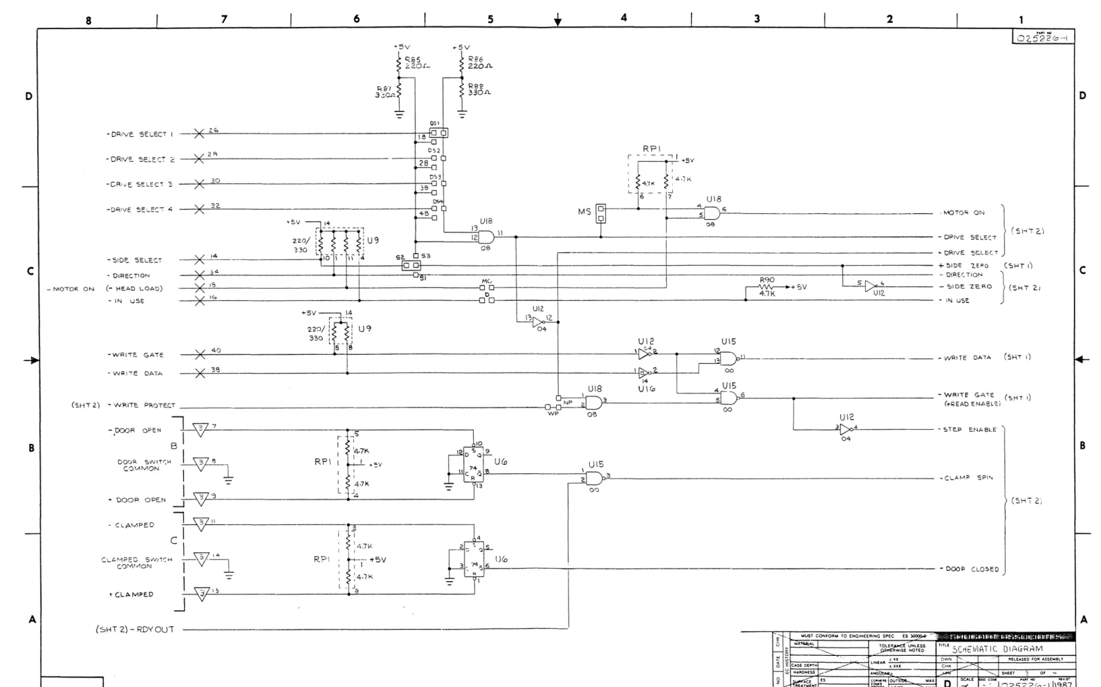
FIGURE 6-1. SCHEMATIC DIAGRAM
PCB 25227 (SH EET 2 OF 4) ,
TOLE~UNLESS ~RWlseNOTEO 8 V8 38 \0
MUST CONFORM TO ENGINEERING SPEC
ES~--I o z 3 4 4 5 5 6 6 7 7 l 8 8 5112(11/80) ___ 3
----~+~~~v_;_---.---==-=-=======-,
:~6~~~;;:;~~i~TC:o;o~Loc~ilJ--~~~:-:-:-:--:-:_~
..
:-:=-=~._::-:-::-~_~,:-:_::-:::-:-_~'
__::-:-::-__
:-:::-:~2~::-:-
11-+5v I . _ '
::L.~,41
- -
- - --- -
-::__
,..:1:-
-ToB I.',: TP27
~4J-'-JV;;-o
-0""1.£ : v,sI
'~6·
I
,,~-"v
C,,23 +~'Z.4V
---llij-f-2---~----~
02.52.2.0-1ti' tx:{,>U'"
i
"
.-?r~---t---_-i..---l~:
~
..
f5V 6 +D-~I
330:. .~,
'.>
, aMD •."';> 12 v,2 " '_ _\_3I "-,U_':.'2'
, . - S50-c.40b, - u CR I 0 0 "LOCK- ,l
9
;~8.[\.
11~:003
II
A :-5TCP _ ,'}' Ii. "= -"10 +"",m' " V I . ; ' 4 e '
'\,
~
\ ON OV'T1-'-'-'II~J'O
Z '~
L-DOO"- LOO< :~
~
-STfP 7loH.Cu-- "04/:r---+r:1--=-I'--'b.,=..
=,~3e=J=======-====-====_==_=_==_~_~_~~_==_=,_~~;~;;~3;s~~;;-T1=~J~Q~4L
:
_ _ MOTO' "" "--'L...I0 " " ' ' ' '
T f - - - 4
~
_ I IIN VS[TACH-_
T
I_~~
__
~_~_IN~E .~~~~~~~~~-
~
.O S "ot U274-l
~_i~~'~I~~~~~~~~~~~~~~~~~~~~~~~~~~~~=~·-RDYOUT(SlT3)
-
- -'
- "
I _ ---.'--- II Res -MOTOI'\. Of!'
r-
,0
1
- ---'1,""+5V
I
~T.c"'N
Ul4 <OTS' r---_=======---
I
+SV~"k~.8ny'~
'i"v nOH, (SHH)~
'I
i. I I U'8 _~
~ ~
T
f
RL' Ie +TROYCL] q
f';""v==t==1==1=~======t-:....::..~~=:~~~
I -L-. 9 361
-~ ~E."DY
IO~-'~H
.., U \ ' ,...-J _ .1.2.5MrlL
r-;
!
.N,'-fl----,-r----1-r--,
-1- ·
i
~e-J._
TR ,...< I I ,---2"NO. '0
08
>53-'.." '" " _. .-;,~--
-=-
::..:..;:
j~--~
-IQQI 8»<E--- -
TRUE READyy '
~
_~
.,NO"..-J°o
4i,'1 'leo -2T : " " < OJ" Ullr---YVV--+Z4Vrl
l
I
1~+5V 5~J~
--- - - - .,'5
c:.~CJ
..L 15 74L':l32.1~1
.---!2 ...L . '''51'15 "",P-b-',~~\'8.2
oEl!', , IV\( 47QJ'\. -3~'1\.[\I~
\~!R55"
RSS"'Z"-' "M".. 8 I
~~
...5<CTO' ...-_-:::.3'''-.1 ,_.. , __ '' 4 -~
' po- I ', '0'2 R'OJ G'/3~
"""~
«3\IIJ90n "II
~
I~~
I .. ROV OM"~~v~-
.. 0 "'" -<", 4.r"... .. 0 ' . To>" W '•..
",T ..L~
2N""A '2:~
, - - - - I~ r-~:
YN5/-" z.I
~
::";"
.,
~
- I 7 7 _ I~"
::,:-S
-nn
"NOE' /seCTOR¢
~
'-'+--0..:.":.J"
[email protected]\C'-@T-P-i-3J..11
- - 2 .05
\ U I 3 !: 17
/.1.!L....~
- -
T "Ii-J
(5H:':~E'/S
..
[;;;R\~
I I
_
7
1
T
Ln"N/-CUTM4'31-':7:
4
'~ L'~~1\9t20
- - t - - -
--=::~
I
F
L-=R=tP=+=====~========jj
I
I I
.£ " ' . " H G c ' ZS e eC~2\
---~
_5 \i7 I{
"OOQRC'-O'EO- +1 0 w'"'O-"
1e-1 ' "
'N"''' __-~Sl!4
I(SH )
=======~=====~=tp~=3=====~========~~f-=~'1£=§=~J=~~~~3
',HO' -NO,,-~
- - - -- - { < X I Z . @ i 'Tl
+
DRI" SUELT ' -.---rT,-h----=:...-.-...:\~4-j
- -y~.
+
}~_":"O
':'0.::9"
DRIVERI: - -- - - !:..
_ I
~
-POR-_ STEP
ENABlt_~j~~======+~ij==E==========~B====j45
I
-lIJI_ - - ..JI -DC -wp
OJTt-'~-':l_---.J
- - _ . - . _ - - .-TRACK" 5 3 40 -TWO 7 , - - ' - 12 U'O
--TRACK~O
(5)<1 ,)-tWRITE PPOTEB 3 3 _ _ f-->- -,-_ _-!--_ - - - ; : TD5 510E,D
::r-:-T----~T~~-Cf-~I~04-v-=--
-~1f'n.!.L·----_··
·W?\iE ?R O-n:C.T(5HT3)
SH1 ,) + REAO OATA _ T - > - > - 1 - - - _ 18 -5'[N • 0 CHG.!Q..- we8 L J <
-~-.-44)~
(~~~~~~~~~~~==~~t~==E======F==~=~==i±~=====~~T.
__
J4~v~_3---~_Z- _~TEP~~
,SHT3) - 'W YT • • n
--~.,
-u0-- '0:?~
(
+REAO [NABLE 3<.. OUT
","_~
- - - TVI/O'HT 3)
~
-- ,---a~
oc - SlOED~
_ =
2'~:C~'-O~
_ 30 'W"N ,~~,
lR.~
-LJ0---'-
Z ) ( - DJ'; T;:l,":'r) DCi
.~5~
+5y-::-1
1
- '
I~-~
C+::l
+'[.
,38, L~hi.r3
~4~2.~~~'
KCHAN~e:
'- - - V
~
J..DATA..---T---t---~---
~
/"(_. -"\RACl< r/JI R I TP2 • • YI CJ 1'\54 ."P-Pi J.L -- -- - - 10 UIOh 8 - - - 5('
I 57 6 TO 2" S.'H'"T
~IM
._ _-!- J.. oJ '-..L: +-TRK,1J LED __
5:S7~---Al~.2.fl:
1 ,., • L +s<ceL... -T~---.
- 7\-~EPARATfD
(LOe"I
_--y--___
~ICi"·{2.
r~+--+---LI.
-- __,-+__
+_~
__
=J::=:
--
"\8~L
, _TR'
~
cEO-W~
:
+.\/-. Y" "NO Ii 1 7' - - SEPARATED DATA: + -, R5S l ' I [ ' " ] ' " , -
~-
_-1:4~113- 2240~f-·
-SECTOR.: W? LED.
1
.3 5
~5~v-_.n..
_ _. . L : L__..__.~_. ~.T-=====---~-+---'-'
~
1"0 8 .L---t--~.-113:~.UB
11----!~.2:_~-I A I 1
11,--===========~-t=========B======
UI5 7." - -INDE<, _w.
L[O 3 2,4 I I - - - , -I
!
WP DETJ
3:~\~~~~~======~L
1:'
-
~
-
- -:::.-.
T~
_ _=.=.=-=====---~-.j.~-+I-LI--==r-
-
~~
I I
-1+~7~V~.:---tF=====r====-"-
----'
1
I 'NDex on
'_D:?
'
-'---===---I COMMON
_~_I_O_!
1_8 ..l. 1~
R&.>4II
,====--
---I INDEX DETDI ' :;,41K <3un - - ---=·'I....J--t---·'?
I
~UPPLY....J
3;1_'3_._20-"-- L 1 : t~"--±:~--M'-·---~l-=-===--=======]
9 0(, '0 1\ U'C.7I + ' 059 _ I
~
_ 2 ' - I ":...,I
'2 02. >3I \NOEX U:.D¢ 1\874
li?~
I -.fID _._--~---: BT'y----VVV-
~
I-: -INDE.X LEDS I 8 ::
U :
~
~,- ~~o
----.---.,,--.---..---I ---"'C
Q~
-: +,NOCX LED I .1.5'875
f,""on
r l 'l
.J
II-
...J~
-:!- : >~_~~~~OR_~E~T_RONlcsl
7:
I'
~
-MOIORON-(SHT3) :- DF<IVE SELECT
l
(~HT 4)(SHT 3) -CLA'''P,... ~-;:,PIN
B
A
c
8 7 6
"'5v
5
... 5V
4 3 2 1
02.522(0--1
o
'<85
2.20.{;... 22.0.fl.R86
o
051
c
CSHTI)
} (SHT 21
... IN U5~
+SI1)E l.ERO
- DIRECTION - ,::>IDEZ.ERO
_ _ _ _ _ _ _ _ _ - WRITE DAiA (51-iT I)
U\5 UI8 08 14·7 K 4.71'< 6 -RP\
" - ., I ..sv
U\2 ---'-1' ~~4()_Sic---1~---'", MS S3 62. U9 14 +5V \4
r' - .. --..,
'220/1 i U9
330 I :
L I 5- 8 220/ 330 +5V 40 36
-*_J.±._. ...IO-'- 11;4
)( "<l
. . L D g r + + . + . _ ; : : ; : ; : ; . . . T--*.
..!.:1~2-..---4-_+---UD·--4t~~---+---o' n 1 + +
-- wRliE DATA - DIRECTION
-WRIIE. GAlE
- SIDt:. SELECT - DRIVE. SE LECT I
- DRIVE. SEL.ECT 2
(- HE.AD LOAD) ... IN USE:
- MOTOR ON
c
A B
\987 RELEASED FOR ASSEMBLY
- DOOP CL05ED
TITLESCrit1vlAT Ie DIAGRHM
MUST CONFOR'" TO ENGINEERING SPEC ES~
C§ CASE OEPTH
o
z
...CLA~"P SPI~
(SHT2) '" :r u 3 4 UIS
---==:r
·\-..:::6:....-____ _ . - WRI\r GAl E (,::>HT I).---2L.J'
L
(+READ E.NA8LEi00 U\2
~.---:,TE.P E.NABLE
04 14 U\<a 4 :3 00 U\5 tHo U(o 5 6 r- ~s I I
I 14 .71<.
I
RP\ I I +SV I I
I 4.7K
L -J 4
7
t CLAMPE.D - CLAMPED
UIB
- .DOOR oPE N
l-w-
7: . .-8 1
DOOR SWITCH
_1_\)7
81
C0~J1MON
I
-... DOOP. OPE.N
--.J~-'3=---
~.---1"""'----c
II~~4"~
\37\4 I
CLlot-'1.?ED SW/TCf-4 ---'V"~ R ' ? \ - - - +5V
Cf),-.;\rvlON
I
-L I I:4.7k
+--w-1-:o,---
..JaJ
(SHT 2) - RDY QUI
8
(SI-i\ 2) -\lV?'IIE. PROTEC.T ---Lw~p'---"""0-8--'
5112 (1\:801
A B
8 7 6 5 4 3 2
o
c
A
B
TITLESCHEMATIC DIAGRAM
. w.u: 0
(51
t
T
• cO~07:F%24VR
TPl4
_ _ _ _ _ _ - iACI-1
2
TOLER UNLESS RWISE NOTED R69
II<. 1'70
- - - ----
----"'UST CONFOfII,l TO ENGINEERIHQ SPfC
Ul
~o
oz
3
9
4
R77lOOK 1"10
2.2.K R78
\1
7
e
DC MOTOR
I
[DC
POWER DRIVERMOTOR,--_._-~~~C~~J
5
..---+--- ._---' C33
I·I-<1F
_---. 1=c.t3
I
C29·~~o3A R7G
lSK +24\1~ - -
-_-J'\.""""-.... 5bO..n. +J..C3\
R75 C32
I
f .7/.(.f'1
·0\ 3'5Vzo~!,
- - ; - - - . . I \ t \ i I \ r - - - j H - - - - t - · - - - .
s
D
-= 5ILICO~IX.
174
_._---,
6 R74
n.SK 1%
101(.
R70~
IO\<' R7\ ~
1<73
IIOK
1%
+24v
1---RlO?
J
c.cK
I
t5V
5
7
C23 .002.7
1- C2.4
~ T .0027 - - - . : : " - 1
L
< ._+Sy ..._
-8
S II 2 (12179)
(SHT 2) MOTOR OF F
P.U.
10
12 D S '}
I
~ Ui~ II C Q8r.:-pOR-_ _+- ...R_13_-t-:=_._
_+_~
JJ
I(~HT I)
I
PHASEi
r-~E_TEC_T_OR_,
[ .--1
L __
B
A
c
o
FIGURE 6-1. SCHEMATIC DIAGRAM,
1
NOTES: UNLESS OTHERWIS 02524'7-0 SPECIFIED
I. ALLCAPACITORS ARE IN MICROFARADS
SOY}+80-20% I
2.ALL DIODES ARE IN4148.
3. ALL RESISTORS ARE IN OHMS,I/4W, 5%; D
1% RESISTORS ARE 1/8W.
4.-0--0- INDICATES CUT-TRACE. OPTION.
5.-0 0-INOICt\TES StlORT1N6 Plll6 OPT'OH
6.·~ INDICATES SHORTING PLUG
( FACTORY INSTALLED).
7. DISTRII:3UTE 0.1 CAPACITORS ON +5V AND +24Y BUS LINES.
8. NPN TRANSISiORS ARE PART OF CA3083. 9. PNP TRANSISTORS ARE PART OF TPQ~906. 10· INDUCTORS ARE :!10%.
2 . -R2.~ 3 4
leB
I-t-
c'1 R2'2. Llto.
1
.1
4 .1IOO)lh ":" 35Y
390 .1 2D%
y y
0 0 <:4' I
IOC-PF 0.\ -'- c5
R2":3 SOV,l?% """S601'F
3~o
>l ~o~
\.:2- 0./
IOO)..lh <:0 R14 R"2.S>
21<. (2.K
5 6 7 8
o
Bc
7 5 8 5 '7,/4 GND 3,8 B 14 \4 7414 Ij\(.,75" 462. U 2.1 LM339 U26
7404 V\2
592N UI
74LSOO U\S,24-,27
74 32. U 25
I.e. TABLE
TYPE POSITION 0u¥PD-f~~E
7474 U20,22.
7408 ut8
16271-1 VI:'
74LS321 u\7
'51420-0 U\4
220/330 U0
ICo278-0 U2.
74L'SOe. U6
CA308'3 u4
iPQ3()O(, uS
lCo270-\ U3
UP(I04-3C U2~
ULN20,"S8 UII
B
c
R\ \~ ~60
CRce L ~ _
A U5ED ON ASM
- - - ~ ~.. -OA 02524-7 -0
1
FIGURE 6-2. SCHEMATIC DIAGRAM, PCB 25247 (SH EET 1 OF 4) TOlER"NCE UNLESS
OTHERWISE NOTED
10/?>~C
MUST CONFORM TO ENGINEERING SPEC. ES30000-0
"'''TEIII''l. "-'ADHEM CI.SE DEPTH R44 2K
+~
t
R45 -@4
~2\<I
"1~4---4--- POR
U4 (SHT'2,3J4')
\'2.. \'3 3 R~6 IK 4 R~? IK 7 U4 ~b 2> 5 REFERENCE DESIGNATIONS LASi USED ~OT USED
C'36 CRc3 Q II I('7~ TP 21 6
/ CHASSIS GND
----'.2;--=---+-.-.--.-....--.
----'.2~3---1f--<T~=_....1----+--+5Y
----'l\'D-''V--·~+ ")...4Y
1:l4~7 .1C 39 (i) TP\e: T50Y
T·
OIT
- - - - ' . 2 2 [20% 24VR8
5112(12/79)
D
A IC 1
-. READ DATA - INDtX
B
- T'vvO 5\CED
- iRACl"- r/J
TRAC'r<."lO (SHT \) -WRITE ?RO~c.T(5HT3)
4'0
1
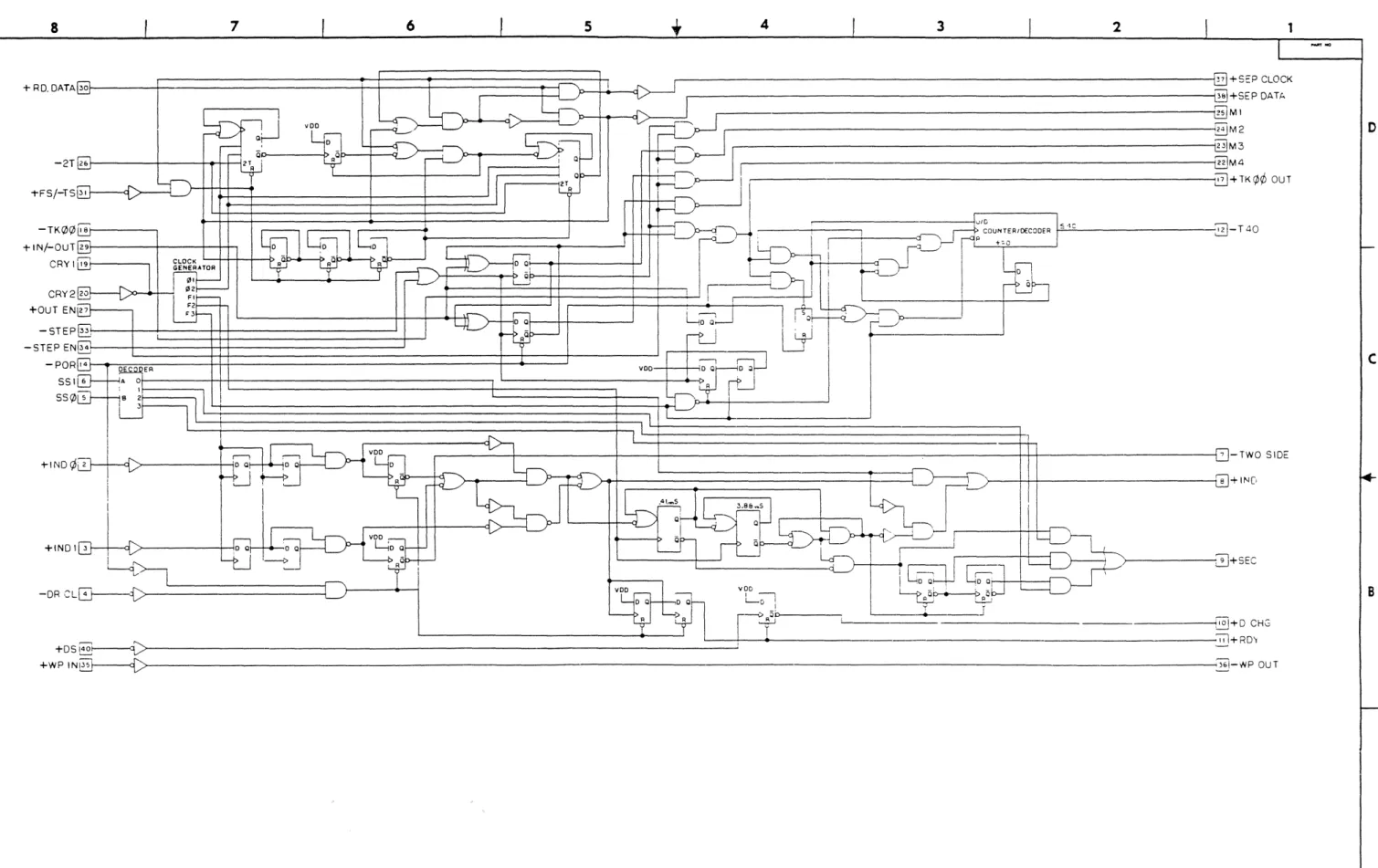
FIGURE 6·2. SCHEMATIC DIAGRAM. PCS 25247 (SHEET 2 OF 4)
Q4 Z:>.1.2.22.A I -I 2 -, 2 12 13 ~ \! s 1 10 8 C7 VB 38
MUST CONFORM TO ENGINEERING SPEC ES~/ "A~L TOLER'u/c£ -UNLESS
j)l'+<ERWISE NOTED
w
~ CASE OEPTH
HARoNess .-o z '" I U 3 3 ,...---+--+---u-t-O---12. 4 4 C~2\ IN4<:>03
{4l<)Z4 !STEP tot10"roR DPiVf-R
I
1.-...-<11--_-..._--.:./.!::... _ . . _
b...!c...=+---__+ + _ .
-~
_ _ _ _ _, ~~13:::---...J
U6 Ll6
UI~
1"1\ ~5'
33 "f":oTEP
I
1.7 I
,.OUT EN
2~:
,=S¢ N\3
6 55 \ 1
Ul3 '2.'2.1 N\4
2.9 '<-'N/-OI)T
2 - !NDrj 1'2.
~- -
--T<;'o 3 "IND \
14-- POR '::l
-WPOUT
4
- DC. 04
-TWO 7
<¥l .. DS SIDED ~ 8
uta
34- -STEN -+D C\o\6 \0
:8 -iK~ 1"7
35 +VVP IN 30 .. RD I':' OWl RS4 1M
2.1) CI':lyL
5 5 YI c:::J SMH~ Ul2 • TP25 1\
nOl-\1~2=----
_
+uT5I--L--+---+---:.~===================~ +---_-_-__--__--_-_- _
TPe:6@
... 145/-55~z4=-.----l--+---i--~~
- RDY OUT
(SlT
3)-M')TO? OfF
r
--..:=~~~3~8~_I_---~;[ml---c;Q"C~.---::::--::::::----.--- 72,0 ~r. 5H I
R
~:...-+--...~-RE,~DY
.,.,:\DY Ow, .::9'- -_-=--=--=--=--=- ., ... . ... ---"1---j----:.-r;--;-:;- TR.
~ a ) ( _ - TRu::; Re>~D'r "
-_
..~ +lIQiOR 0NO-.IT 6 6 - POI'< 10~ROY \1'\23
I")
'1 4.U27
:I9JYl
O_?9__E>~:_+-_I_+_---..::....---:=--_-_---I
=J
5 - - SIDE. "ZERO(~1T:')
l l + t t n r
-.-::::-1 VDO 'K4G 41l'\ 12 -MD -<;,TEP MOTOROl" 4 -DS
3 _INUSE
16 Ul4
TA.CH IN
, + I r
-
l---+---,--~---+---_t---
---_._---,----:-AC.TIVIT'{ Lt'SHT , ClaORI:OOU'l
: SOLE-NOlO DRIVE.R _--..-J~"''5V
: 10 ut9
I
I~O.l'l. <::1<.23---1~----,-,----~~re, _--()+---,
: ~\U 2 5 ; ; 8 S5Q--~..:Jo
-::!:-- ORL~l . £ 2 - - - + - - - - · - - - - -ir - - II _ ..- - - . -...-=-L...-'
- - ' - - \
' ~2._ _ _ __ _ _
7 7 -+Sy"l I 1 1 I I I R5B 150n. 2,4 L3
~
IOO.llHS
2, \4 Y2 .r-5MHz c:::JTRr<.~DE.T
m..:.
I . _...- v R.57
~5 1.~5~OSl. t-TRKrlJ LED - V - - v v v - - - - 4
8 -TpK1> LcD 8
15
- - , ::l 5
+W PLED I ~'I-..:::--.!VII\r--+-....
AI
- wP L E:.D I 3,L...:.2~,=4 ...
I
WP DET
...J1W-'---INDEX DE T
J_'\JV
12,.!.::14-!..- - 4COMMO"-l D ~
INDEX DEi ..lm...:.15::!.l.!..!.:\6~ _
SUPPLY -J-v R59
:J \874 \~~~
-r\NOEX LE.D¢~vvv.--+--'"
B
-INDEX LEO~ ~~3,-- ~
+tNDE.X LED I I 8;-..:.,----,,\IV\,r--'
1 -.J
: ISE.NSOR ELEC"TRONICsl
L , _
,---slia(11/80)
-STE.P
{
MOiOR O N
-(:'HT3) -DRIVE SELECT----+---~+----+----...:.q
'-IN USE ---+---4
(~HT4\ TACH
B
A C
D
8 7 6
• R.eS
• 22.0..n..
....-R.87 > 33o.n.:>
5
-t-5V
R86
: 220.0.
~
Rgg
~ 330.11.
4 3 2 1
02524-7-0
D
c
(SHi2.)
(51-lTI)
} (SHT 2)
+SlOE l..ERC - DIRECTION - '::lIDEZE.RO
- 1\\1 U5E. U\8
RPI
r .- - - ,f i"5V
I I
:
~
• : 4·7KI >4.7K I
L-6--~
UIZ
~
04-MS ~~ 4
5. 1 \ 1 - ' - 6 _ _ _ _ _ _ _ _ _ _ _ _ _ _ 'I
Ule iI _ ' -N'OTOR ON I
13 08
l'
121 ' J r " - . , - - - + - - - l - - - · - - - - - DRIVE SEL'i:.C.T
06
r - - - + - - - - · - - - ;.DRIVE 5E.LECT
-t-5V \4
r- -~l
220/
I.
.
1 U9330 I I
L I
5- I
B
U9
OSI
lB~~
~
O~2
-~~':""-_---'--'---+~-2'ea
D~3
- SIDE. SELE.C.T
• OIREC.TION
(- HEAD LOAD)
- IN USE.
- MOTOR ON
c
-WRITE. GATE
- WRITE DAiA (SHT I)
- WRITE DATA
(SHT 2)
- WRITE GATE ($HT IJ2 )
U\2
' - - .3i1.1
4-04
B 5
6 1120
UIS
00
- SiE.P ENABLE]
-DOOR C.LOSIO:D ( SHT<= )
- - - -CLAMP SPIN
B
(SHTe) - ROY OUT
A A
5112(11/80)
8 7 6 5 4 3
w ~
c
o z
RElEASEO FOA ASSE ..SlY
199"3
1
FIGURE 6·2. SCHEMATIC DIAGRAM
8 7 6 5 4 3 2
o
o
c
~JIYYL..,
I
W\N\)\~G5MOiORj R<03
~ IK
+sv
Rg2.
~OOk 1...-_---'
;'-:::'--+1--'-
.1--=C-24-:---+[_9=--i~
141
10 T
.002_7._,
_20_0_V__,\_O_% ....:B~V9 I .
L
_
I 1. C23
9 \1 I T .002.7,cMV, IO~
I
c
I
9 5
(SHT 2) MOTOR OF F
B
A (5HTV
2 1
FIGURE 6·2. SCHEMATIC DIAGRAM,
PCB 25247 (SHEET 4 OF 4)
ci
z
3 4
t
5
6 7
8
+5V
w
!(
Q
5112(12179)
~~l
• 8~~~-~~~~:~-~==~~C-~=2-'-O~I~~~-R~~=0=~-~-R~~-7~::~-====-~~~~~~-~~~~~~-~~-~~----~--~~~~~-=====~~~~~~-~===-~-~_-::::+-a-~-~--~CH
<$
IIIII
;;?
!
.~;;
I,~~;~~OK
150K >RCoB1.<T!F
8I
">~:
Q5I
>IOOK 2N2.907 C51
':1 9
-=t---1
4I
Q~ + c55 t 4.7J,1FI
~~:~~I---~I~I~
__
--_-~---~---~---~~~~~~~~~~-::I ~3 ~
IR79
~K~P~:~ T~~
I
'2~9 I~ ~754(O2
D <R~?
J
t
;;;>Q I > ":>-:>L;' IS IK ::>AVR
~
U20I
12 5'0 9 U21~
<~'r::
13 NEe J.-,:..:;I°-_-1
'VV1r-..._+-+l Qi22.222A l..'"t"I
74
~Ir
_
~22
- r 2DS
4- r-2.I
1
C29 \b /2R80
G~
TP[4720Hr:-"C
alB -
74 _ u22I
~cii"> 'r"'·~~ojAF R7~ ~ j.APCI043C C34 IK ?R82. "RS3 R84I
(SHT.2) '---t~,--u
C
l"">Q~ -74
,
% ~--..J\1",5I\rK_...1+24"--"sl'.blVo.ll.-+---lc-3-\-+----:...je ~r·
047,((F
:>3<J()..(l. "S.\K: 8.2.'5K1'7
0-~ ~
~~~1
I:
lJ.5K-
~ I_"~ ~
-=
..
-~--_~====:~N7-~~7-K~-I~~O~-~~-+II-~-~-o---~---~--
-_~
__
~
III) 1%
I
I
R69I
r-~~~
J
775M
T;~tR71
r,-D(r~~
:~:
I
1~~~E~T~~\vERI
~'~
1%I
•
U21 d /0,"<;{j-~SQ~'Lr'~~>JIX
I~;~~~J----
-i-' - - - -
----I
L -- -- -- -- -- ----
U TITLESCHEMATIC DIAGR.AMA
8 7 6 5 4 3 2
A
c
B
l;.'jED ON AS""
-CA OZ524C;- I I.e. TABLE
TYPE
POSITION~~~~~ vce GND592 UI 10
..2-1~278-o u2 - 5
1Go270-1 U3 10 3
CA3a:e u4-
-
-TPGl~Ob us -
-7474 U20 14 7
7438 U7,8,IO,I9 14- '1
220/330 u9 14 7
ULlf2ob5S UII -
-74D4- Ula 14 7
16271-1 U\3 I 21
51420-0 Ul4 I 13
i4LSOO U\S.24-
.,
14 77414- Ull. /4 ...,
741-5321 U\7 \6 8
7408 U18; 6 11 (U6) 14- ...,
UPC.IOfr3c Uc~ - 8
LM~39 u26 -
12-74 32. u25 14 7
7546c. U2..1 3 8
4-TOI.ERANCE UNLESS OTHERWISE NOTED IoIUST CONFORIoI TO ElIGINEERINQ SPEC. ES3llOOO-O
2 R44 ZK +?V \3 --~ PRODuCT
o CASEO£I'TH
~..:....j.;,-+:-~+--i r.;.HAIl:.:.=;.:OHE:::SS+ -t:A::::"O~lJL,Ul::r"~--_+...::.::.::~~~~~:.:....:*~--:;;l;=_i
~~~HTr-;.ES~--~:5: ::MlE WAX
Rs5 IK v v R~S IK 4 7 U4 ~b TP4
1
~----4--- PeR
14 (SHT2,3
J4')
U4-\'2..
I _
L ~ _
G,9
RII,GO,(i,5,8~i~
TP3,S-7,11,15
17 - 24
5 Q II RI02 TP 21 U26 J9 REFERENCE DESIGNATIONS LAS! USED iJOT USED
G c:56 C50
CRc3 CR22
6
R8
lOOK
...---l...---'\vAvrv"v--+z",V
RtD .I e3G
'>2.41<.
-=
0.1~R7
(>Z.4K.
CHASSIS GND
+5¥
. RI3 RI4
,4.~K 17.4~
RI2. IP/D 31%
~.37K
zR
US1% +c:;,y
----"wf--
I--JSn-C-3-9---~-.-;:~v
Tto~
1.
01
_ _ _->.,z.,L..=2:...-..__+=::l:::J.o~o/L::."o~ """,,,,,- 2.4VR.
- - - - \ 1--=3:...-...J. l--_+ 5V
TPG5,<:;Cfl,GrISJGI<':',GF
•
8
SHIELD 0
SIIZ (12179)
SHT 2)- TRA,(.\( 40
.-- ...- , --. ... ..._..- -...---JvRII\~8r__ +Z4V 025~49-,
I
1
1-1' ~ i70 NOTES: Ut-.JLE55 OTHERWISE>RI C3 C2 R4 ~ C8 l:Cq CRlt? TP2. \W
5PECIFIED-I '>1 5 0 ,0.1 0.1 4.7K. : LI
J_
0..1 14.7 INt:..2.4"C./ ' - 1 7 .~ CI.9\ I. ALLCAPACITORS AREINMICROFARADS.r - - I R.2'2. lOO)lh -=-35 V __ I'2V> S% O.
">-iJ-6 I ,'R2
-iT
~7
~
CI 390 _ , , 2 0 %4~ ~
50VJ+80-20%---+--?> 7 >IR~ - I ' \ 2.A.LL DIODES ARE lN4148
J ( -=- I .?
>-;; -
v """"'0 I1
TPI L!.:!: 10Q -=b ,12K . 22k - 022 I . - J C4 00~_ _..., 3.ALLRE5ISTOR5AREINOHMS.V4W,5%j 0
Rjw ¢ I
I~R/wQil
4 CRI I I~~CRII ";~RI1
CRI3\~50VJ(],J.
R2.3'r'~:~%
0.1Ti~oPf'
(i) UI5q22~
,I
I%RE5ISTORS ARE 1/8W.I / / ~ \ -=- r1 3~o ~o~
T
~Jl "13 CI8.l 4-0-0- INDICATES CUT-TRACEOP110N.I
~
I 3 CR1 I .>R5 I 3-L?
RI~PI~
0.1, 5.-0 D-INDICATES SHORTIN6PU~
OPTIONSIDE \0CT I
~
I / / I S4.87K 1c56~2
17 L-z. hO~ ~
R14 R2..S> R2.t -=- • 2.4-1(6.~
INDICA1ES SHORTING-PLUG.: t /
,,2. CR3I I I% T82p~
2 16 IOOfA C 2.K >2K (10K R'--17R?flt~
9ifF
(FACTORY INSTALLED)./ ~ I 4 i.U« 5 oJ/ RI5 7. DISTRIBUTE OJ CAPACITORS().J +5V
R/Wrj
2.:
1~IEDID01:
I CR4 I C.7 R 3" 200 IOOKL 0 I K AND +24V BUSLINES.I '- 8.NPN TRANSISTORSAREPARTCfCA308.3,
I ~>-h
1
R18'-~ I ' - - - ! I C.RION _ I 0.1 10K A A 9.PNP TRANSISTORSARE PART OF TPQ3906.
ERASE0 I - , l./T -'- r---"ZV\OOtv--+---J 10.INDUCTORS ARE :t10%.
::II~T
!~--- :~: ~
l
[READ
CHAN~
-~r~~I~~
@TPI6I I , , : ) CR7L I
cia
7 DISFFIN DATA 0I
::~:EI
!
~ ~'fld:
J7
~
:--- --- --- -- - --- -
---r----
---l
R2;24V
ISOP~~.V~~~:
U2
OUTt--::---+--+~f~'A
I
~
~
" " 6 c..R'1 I I I220~ R2~
CII 052 16<':78-0L- - - - __ .J / / I 1..-'1 I I
I
::1.1J. / 1..
m}l.t>00/' 9.531(~I%> L_JL-§-hS2~\--:2JV. 6ND~I - LSHIELD I
/rll
tb\D/WRITEII CIS +'?V I .(