Implementation and Analysis of Cascaded H Bridge
Multilevel Inverter Using Space Vector PWM
S.Narasimha
1, Ala.Madhusudhan
2, J.Lingappa
31
Professor, Dept. of E.E.E, TKRCET, (India)
2,3
Assistant Professor, Dept. of E.E.E, TKRCET, (India)
ABSTRACT
The implementation and analysis strategies plays vital role to minimize THD in Multilevel inverter. The
modulation technique regards Selective harmonic Elimination and Space Vector Pulse Width
Modulation(SVPWM).Multilevel inverters has tremendous application in the area of high-power and
medium-voltage energy control. In this paper simulation of SVPWM is performed for cascaded H bridge Multilevel
inverter . Simulation of three,five ,seven, eleven leves and thirteen levels cascaded H bridge multilevel inverter
with Space vector PWM has been carried out. Implementation and Analysis are presented to realize the validity
of the Total harmonic distortion.
Keywords: Multilevel Inverter, Pulse Width Modulation, Space Vector Pulse Width Modulation,
Total Harmonic Distortion
.I.
INTRODUCTION
Numerous industrial applications require higher power apparatus in recent years. Some medium voltage motor drives and utility applications require medium voltage and megawatt power level. A multilevel power converter structure has been introduced as an alternative in high power and medium voltage situations Subsequently, several multilevel converter topologies have been developed.A multilevel converter not only achieves high power ratings but also enables the use of renewable energy sources. The advantages of three-level Inverter topology over conventional two-level topology are 1)The voltage across the switches is only one half of the DC source voltage 2)The switching frequency can be reduced for the same switching losses 3)The higher output current harmonics are reduced by the same switching frequency.
I.space vector PWM technique is used for variable frequency drive applications.It utilizes DC bus voltage more effectively SVPWM utilize a chaotic changing switching frequency to spread the harmonics continuously to awide brand area so that the peak harmonics can be reduced greatlyease of use.
II.BASIC PULSE WIDTH MODULATION TECHNIQUES
i) Single Pulse Width Modulation:
carrier wave the gating signals are generated as shown in Fig 1. The frequency of reference signal determines fundamental frequency of output voltage.
Fig 1.Single pulse width modulation
Advantages:
1. The even harmonics are absent due to the symmetry of the output voltage along the x-axis.
2. Nth harmonics can be eliminated from inverter output voltage if the pulse width is made equal to 2π/n. Disadvantages:
1. The output voltage introduces a great deal of harmonic content. 2. At a low output voltage the distortion factors increases significantly
ii) Multiple Pulse Width Modulation:
In Multiple Pulse Width Modulation several equidistant pulses per half cycle are generated as shown in Fig 2. By using several pulses in each half cycle of output voltage the harmonic content can be reduced.
Advantages:
1. Amplitudes of lower order harmonics are reduced. 2. Derating factor is reduced significantly.
Disadvantages:
1. The fundamental component of output voltage is less.
Fig.2. Multiple pulse width modulation
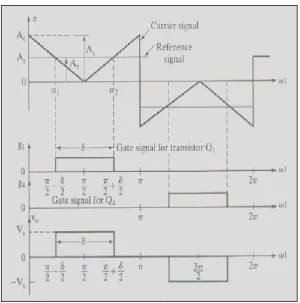
iii) Sinusoidal Pulse Width Modulation:
In Multiple Pulse Width Modulation, by varying the width of each pulse in proportion to the amplitude of the reference wave the distortion factor and lower order harmonics can be reduced significantly and the width of all the pulses are maintained the same. This type of modulation is commonly used in industrial applications and is known as Sinusoidal Pulse Width Modulation.
By comparing sinusoidal reference signal with a triangular carrier wave of frequency, fc, the gating signal is generated. The inverter output frequency, fo, and its peak amplitude, Ar, determines the frequency of reference signal fr and controls the modulation index, M, and then in turns the rms output voltage, Vo. The number of pulses per half cycle depends upon the carrier frequency.
Fig.3. Sinusoidal pulse width modulation
The distortion factor is significantly reduced compared to that of multiple Pulse modulations. This type of modulation eliminates all harmonics less than or equal to 2p-1.
For p=5, the lowest order harmonic is ninth.
iv) Advanced Modulation Techniques:
Trapezoidal modulation:
By comparing a triangular carrier wave (Vc) with a reference trapezoidal wave (Vr), the switching instance to semiconductor devices are generated. This type of modulation increases the peak fundamental output voltage up to 1.05Vd, but output voltage contains lower order harmonics.
Fig.4 Trapezoidal modulation
v) Staircase modulation
In staircase Pulse Width Modulation the modulated wave eliminates specific harmonics. In order to obtain desired quality of output voltage, the modulation frequency ratio mf and the number of steps are chosen. If the number of pulses is less than 15 per half cycle this is optimized PWM.
vi) Stepped modulation
In this modulation the signal is stepped wave. In order to control the magnitude of the fundamental component and to eliminate specific harmonics this wave is divided into specific intervals, with each interval being controlled individually. When compared to that of normal Pulse Width Modulation control this type control gives low distortion but higher fundamental amplitude.
Fig.6 Stepped modulation
vii) Harmonic Injected modulation
In this modulation the signal is generated by injecting harmonics to the sine wave. The result is a flat topped wave form and it reduces the amount of over modulation. A higher fundamental amplitude and low distortion of output voltage is provided. The amplitude of fundamental components is approximately 15% more than that of normal sinusoidal Pulse Width Modulation.
Fig.7 Harmonic injected modulation
viii) Delta modulation
The fundamental output voltage can be uptoVs and is dependent on peak amplitude Ar and frequency fr of reference voltage. This modulation can control the ratio of voltage to frequency. Depending on the permissible harmonic content in the inverter output voltage, machine type, power level and semi conductor switching devices employed for a particular application, the particular Pulse Width Modulation is choose.
Fig.8 Delta modulation
ix) Space Vector Pulse Width Modulation:
This modulation is relatively new and popular technique in controlling motor devices. By combing the switching states corresponding to the basic space vector, the reference voltage is approximated. The main advantage of this technique is that it will generate less harmonic distortion in the output voltages and currents. Advantages of PWM Techniques:
Using Pulse Width Modulation techniques lower order harmonics can be eliminated or minimized along with its output voltage control. The filtering requirements are also minimized.
Both the output voltage and frequency control is possible in a single power stage of the inverter without any additional components.
The presence of constant DC supply permits the parallel operation of several independent Pulse Width Modulation inverters on the same rectifier power supply. Pulse Width Modulation inverter has a transient response which is much better than that of quasi-square wave rectifier.
III.SVPWM SCHEME
Space Vector Modulation(SVM) is an algorithm for the control of pulse width modulation (PWM).It is used for the creation of alternating current (AC) waveforms; most commonly to drive 3 phase AC powered motors at varying speeds from DC using multiple class-D amplifiers. There are various variations of SVM that result in different quality and computational requirements. One active area of development is in the reduction of total harmonic distortion (THD) created by the rapid switching inherent A three phase inverter as shown to the right converts a DC supply, via a series of switches, to three output legs which could be connected to a three-phase
motor.
The switches must be controlled so that at no time are both switches in the same leg turned on or else the DC
leg. i.e. if A+ is on then A− is off and vice versa. This leads to eight possible switching vectors for the inverter,
V0 through V7 with six active switching vectors and two zero vectors.
3.1 SVPWM SCHEME
For an n-level inverter the output voltage vector in this paper is defined as
whereua, ub, and uc are the instantaneous output voltages of phases A, B, and C of the inverter, respectively, relative to the negative terminal of the DC source. When assuming the voltages on the DC-link capacitors are identical, the output voltage vector becomes.
Where Vdc is voltage of the DC source, and Sa, Sb, and Sc(Sa, Sb ,Sc=0, 1, …n-1) are the switching states of phases A, B, and C, respectively. Accordingly, the voltage of each DC-link Capacitor is Vdc/(n-1), and the output voltages of phase A, B, and C relative to the negative terminal of the DC source areSa·Vdc/(n-1), Sb·Vdc/(n-1), and Sc·Vdc/(n-1), respectively.
Fig.9.Space vector diagram of a five-level inverter
A space vector diagram containing all the output vectors and the corresponding switching states of the inverter can be generated . For example, Fig.3.3 shows the space vector diagram of a five-level inverter calculated in this way, where Vref is the reference or desired voltage vector, and Vn1, Vn2, and Vn3 are the corresponding nearest three vectors. It is the task of the SVPWM scheme to synthesize the reference vector as follows
Fig.10.Location method for the reference vector
The SVPWM scheme proposed is shown in Fig. 10. It can generate all the available switching sequences and the corresponding duty cycles according to thereference voltage and the commanded switching frequency forany level of inverter. For purposes of demonstration, theSVPWM is illustrated based on the space vector diagram ofthe five-level inverter shown in Fig.9. The detailed method of generating the switching sequences and calculating the corresponding duty cycles is introduced as follows.
Fig11.switching sequence modes
3.2 SWITCHING SEQUENCE
First, the reference vector Vref is represented as the sum of a set of “vertex vectors” and a “remainder vector”Vref, as shown in Fig. 10. A vertex vector is a vector connecting two adjacent vertices. The vertex vectors connect the centre vertex of the n-level space-vector diagram H0 with a first vertex of the “modulation triangle” (composed by the vertices of the nearest three vectors Vn1, Vn2, and Vn3 as in Fig.9). The remainder vector is the vector enclosed by the modulation triangle and connecting the first vertex of the modulation triangle with the reference vector.
One way to determine the set of vertex vectors is based on determining a set of nested hexagons H1, H2, and H3enclosing the reference vector, as shown in Fig. 10. Each nested hexagon corresponds to a specific level
vertex vector can be selected, as the blue solid arrow shown in Fig.12, and the origin of the reference vector is shifted to the vertex of the selected vertex vector, which is the center vertex of the selected nested hexagon H1. The other nested hexagons can be selected in a similar way.
Fig.12. Selection of the vertex vectors and nested hexagons
Second, based on a function s of the angle φ of the corresponding vertex vector relative to axis A, determine iteratively the switching states at the vertices for each vertex vector in the set of vertex vectors, starting from the present switching states of the inverter at the origin vertex, by modifying (increase or decrease by 1) a corresponding phase of the present switching states to produce the switching states of the inverter at the first vertex of the modulation triangle. The function s of the angle φ (0 ≤φ <2π) of the corresponding vertex vector can be described as
S=3 +1 ---3.
IV.SIMULATIONRESULTS
Fig.4.1 Three level H-bridge inverter
The FFT analysis five level cascaded H bridge inverter with SVPWM is shown in the Fig.4.2
The FFT analysis of seven level cascaded H bridge inverter with SVPWM is shown in the Fig.4.3
Fig.4.3 Seven level H-bridge inverter
The FFT analysis of eleven level cascaded H bridge inverter with SVPWM isisas shown in the Fig.4.4
Fig.4.4 Eleven level H-bridge inverter
The FFT analysis of thirteen level cascaded H bridge inverter with SVPWM is as shown in the Fig 4.5.
Fig.4.5 Thirteen level H-bridge inverter
Fig.4.6The FFT analysis of three cascaded H bridge inverter
Fig.4.7 The FFT analysis of five level cascaded H bridge inverter
Fig.4.8The FFT analysis ofseven level cascaded H bridge inverter
Fig.4.9.The FFT analysis ofelevenlevel cascaded H bridge inverter
Fig.4.10.The FFT analysis of thirteenlevel cascaded H bridge inverter
Table1. THD Analysis
Level THD(%)
3 51.21
5 39.79
7 28.45
11 14.84
V. CONCLUSION
simulation of SVPWM is performed for cascaded H bridge Multilevel inverter . Simulation of three, five ,seven, eleven leves
and thirteen levels cascaded H bridge multilevel inverter with Space vector PWM has been carried out and Total harmonic
distortion calculated.
REFERENCES
[1]V.NAUMANEN,J.LUUKKO,P.SILVENTOINEN,J.PYRHONEN,H.SAREN, Compensation of DC link voltage variation of a multilevel series-connected H-bridge inverter.
[2] CELANOVIC N., BOROYEVICH D.: „A fast space vector modulation algorithm for multilevel three-phase converters‟. Conf. Record of the IEEE-IAS Thirty-Fourth Annual Meeting 1999, 3–7 October 1999, vol. 2,pp. 1173–1177.
[3] WEI S., WU B., LI F., LIU C.: „A general space vector PWM control algorithm for multilevel inverters‟. Eighteenth Annual IEEE Applied Power Electronics Conf. andExposition, 2003, APEC‟03, 9–13 February 2003, vol. 1,pp. 562–568.
[4] KOURO S., RODRIGUEZ J., PONTT J., ANGULO M.: „Multilevel inverter modulation method with dc-link disturbance compensation‟. 31st Annual Conf. IEEE Industrial Electronics Society, 2005.
[5] FILHO F., MATEUS T., MAIA H., OZPINECI B., PINTO J., TOLBERT L.„Real-time selective harmonic minimization in cascaded multilevel inverters with varying dc sources‟. IEEE Power Electronics Specialists Conf. 2008, PESC 2008, 15–19 June2008, pp. 4302–4306.
[6] NAUMANEN V., LUUKKO J., SILVENTOINEN P., PYRHONEN J., SAREN H.,RAUMA K.: „Compensation of unequal voltages in the DC links of a multilevel series-connected H-bridge inverter‟. 35thConf. IEEE Industrial Electronics Society, IECON 2009,2009, p. 6.
[7] NAUMANEN V., LUUKKO J., ITKONEN T., PYRHONEN O., PYRHONEN J.:„Equal load sharing modulation technique for series connected H-bridge multilevel converters‟. IEEE Power Electronics Specialists Conf., 2008, PESC 2008, 15 –19June 2008, pp. 3315–3319.
[8]S. Narasimha, Dr. M. Sushama “Digital Control of Multi Level cascade Inverter with Variable DC Voltage Sources” published in Vol. 7 No.1 January 2015, International Journal of Engineering Science and Technology,pg:32-45,ISSN:0975-5462.