Full Length Research Article
DESIGN OF FPGA BASED 8 BIT RISC PROCESSOR WITH PERIPHERALS
*1
Kulkarni, S. V.,
1Shah, P. P. and
2Bhanarkar, M. K.
1
Department of Electronics, Devchand College, Arjunnagar, MS-India
2
Department of Electronics, Shivaji University, Kolhapur, MS-India
ARTICLE INFO ABSTRACT
RISC or Reduced Instruction Set Computer is a popular design which becomes the important part of Scientific, Engineering and Industrial applications. It gives higher performance with complex logic circuitry on a single chip. So the main objective of this paper is to design 8 bit RISC (Reduced Instruction Set Computer) processor by using Spartan 6E tool. This is easy to design and support Load-Store architecture. To important components is designed using VHDL (Verilog Hardware Descriptive Language) programming and realize by using Spartan 6E tool. The important features of this controller are Arithmetic Logic Unit (ALU), Serial Peripheral Interface (SPI), Interrupt controller etc.
Copyright© 2017, Kulkarni et al.This is an open access article distributed under the Creative Commons Attribution License, which permits unrestricted use, distribution, and reproduction in any medium, provided the original work is properly cited.
INTRODUCTION
FPGA- Field Programmable Gate Array is an integrated circuit designed and configured by a customer or designer after manufacturing hence called “Field Programmable”. The configuration specified is normally done by Hardware Descriptive Language (HDL). The HDL contains logic components that components are logic boxes which are programmable. That logic boxes has the ability that cells or blocks are wired together. Nowadays FPGA is growing fast with cost reduction comparative to Application Specific Integrated Circuit Design (ASIC) (Kulkarni, 2016). The important features of RISC processor are the instruction set that is based on hardwired architecture. In that there is no need of microcode for single cycle execution. In this architecture all instructions are same in length and size (fixed in bit). That helps in fetching the instruction from various memory locations. RISC processor works only on load and store architecture. Therefore it has less number of addressing modes. The instructions are operates between only memory and register. That results in improvement of cycle time for execution per instruction. Because of all instructions are same size and length they are easily piped (Uma, 2012). Present research work is based on the implementation of low cost 8 bit Reduced Instruction Set Computer (RISC) processor on a FPGA.
*Corresponding author: Kulkarni, S. V.,
Department of Electronics, Devchand College, Arjunnagar, MS-India
It gives the benefits to custom Very Large Scale Integration (VLSI) design to avoid initial cost and time delay.
RISC PROCESSOR ARCHITECTURE
RISC architecture was first developed by IBM in 1970’s and completed by T. J. Watson at research centre in1980’s. He was started with frequently used simple instructions. IBM was the first company to define Reduced Instruction Set Computer (RISC) and further research was done by Universities of Berkeley and Stanford to give Basic Architectural models (Luker, 2001). All the processors are designed around two techniques; Complex Instruction Set Computer (CISC) and Reduced Instruction Set Computer (RISC). The CISC is the concept that approaches to the Instruction Set Architecture (ISA) which is based on doing more work in one instruction with variety of addressing modes. Due to instruction has variable length, they are generally implemented using micro programmed model (Mishra, 2015), Some characteristics of CISC are as follows.
It depends on Hardware.
Instructions can execute in many clock cycles.
Instruction set is complex.
Memory to Memory Load and store incorporated in
instructions.
Cycle period per instruction is high.
Pipelining is not possible.
ISSN: 2230-9926
International Journal of Development Research
Vol. 07, Issue, 07, pp.13531-13535, July, 2017
DEVELOPMENT RESEARCH
Article History: Received 29th April, 2017 Received in revised form 04th May, 2017
Accepted 26th June, 2017
Published online 22nd July, 2017
Key Words:
As compared to CISC; RISC processor works on simple instructions with fixed length of instructions that results in faster execution of instructions per clock cycle as compared to CISC. Therefore nowadays RISC becomes famous and becomes more important device for computer systems (Chokkalingam). Some important characteristics of RISC processor is as fallows.
It uses hardwired units.
Instructions are small therefore executes in a single
clock cycle.
It has reduced instruction set.
Instruction length and size is same.
It has general purpose registers and simple addressing
modes.
Register to Register Load and Store are independent
instructions.
Code is large but cycle period is low.
Pipelining is possible.
Design of Arithmetic Logic Unit (ALU)
[image:2.595.338.530.377.767.2]The fig 1 and 2 shows block diagram and RTL schematic of ALU respectively. It contains inputs ports 'a' and 'b' which is 8 bit wide and select line 's' which is 4 bit wide. The output is obtained at out1 line, which is also 8 bit wide. The ALU performs arithmetic and logical operations such as AND, OR, NOT, NOP, NAND, NOR, XOR etc. Table 1 shows details of arithmetic and logical instruction operations The instructions designed for ALU are 8 bit wide. Furthermore, ALU contains logic gates, adder, substractor, multiplexers etc for the intended operation.
Fig. 1. Block diagram of ALU
Fig. 2. RTL schematic of ALU
Peripherals of RISC Processor
A Serial Peripheral Interface (SPI)
The Serial Peripheral Interface (SPI) is a serial input or output port that allows 2 to 16 bit DataStream to be shifted in to the device or to be shifted out of the device at defined rate. It is normally used to communication between the device and external peripherals. To connect external I/O’s or any peripheral via display drivers, EPROMS, Analog to Digital converters (ADC) etc. It has two modes master and slave.
Features of SPI [1]
SPI has 16 bit shift register.
It has 16 bit receive buffer register (SPIBUF)
16 bit transmit date register (SPIDAT0) and 16 bit format selection register (SPIDAT1)
Baud clock generator (8 bit)
Serial clock I/O pins.
Slave in and Master out (SPISIMO) I/O pins
Slave out Master in (SPISOMI) I/O pins
SPI clock frequency range will be programmable.
Programmable character length (2 to 16 bit)
Interrupt capability
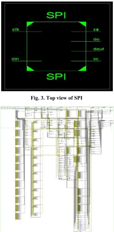
Simulation Results of SPI
[image:2.595.68.260.440.600.2]Fig. 3. Top view of SPI
[image:2.595.49.275.485.772.2]Fig. 5. Timing diagram of SPI
The timing diagram shows that the testing of SPI. In fig 2 Clk =1, cheap selection (cs) is 1, external data given to the input and various conditions are tested for SPI.
B Universal Asynchronous Receiver / Transmitter (UART)
The Universal Asynchronous Receiver / transmitter (UART) performs serial to parallel conversion on data received from external peripheral device and on data received from central processing unit (CPU) does the parallel to serial conversion. The CPU can read UART status any time. It has the control capability and processor interrupt system. This system is used to minimize software management and communication link. The feature of UART is, it has programmable baud generator capable of dividing the UART input clock from 1 to 65535.
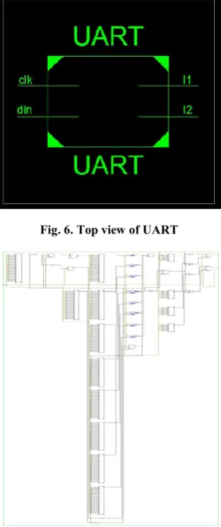
[image:3.595.308.554.52.178.2]Simulation Results of UART
Fig. 6. Top view of UART
Fig. 7. RTL view of UART
Fig. 8. Timing diagram of UART
C Pulse Width Modulation (PWM)
Pulse Width Modulation (PWM) is a technique which is used to vary the pulse width of a output signal instead of varying the analog signal. By increasing or decreasing the pulse width, the controller regulates output energy to the load. PWM is used to obtain variable voltage and frequency supply.PWM is mainly divides in to two types. 1 Symmetric PWM, 2 Asymmetric PWM
[image:3.595.330.538.336.472.2]Simulation results of PWM
[image:3.595.84.242.400.777.2]Fig. 9. Top view of PWM
Fig. 10. RTL View of PWM
The timing diagram (Fig 11) of PWM is shows that by varying the clock period we can vary the pulse width of output signal.
D Timer/Counter
[image:3.595.308.558.429.688.2]external clock pulses and the same circuit used as a timer when external clock pulses comes with same frequency. The timer/counter circuit consists of 8 bit timer/counter register, capture register and compare register to monitor the time.
Fig. 11. Timing diagram of PWM
[image:4.595.69.258.290.454.2]Simulation results of Timer/Counter
[image:4.595.348.520.294.448.2]Fig. 12. Top view of Timer/Counter
Fig. 13. RTL view of Timer/Counter
Fig. 14. Timing diagaram of Timer/Counter
The timing diagram shows that as clock becomes one after each clock counter counts the value incremented by one.
Interrupt Controller
A signal that gives information to a program or a device connected to the processor that an event is occurred that signal is called Interrupt Signal. When a device or processor receives an interrupt signal, it takes a specified action depending on priority which is defined by the user. It can cause a program to stop itself temporarily to service the interrupt by branching in to another program called Interrupt Service Routine (ISR) for specified device caused the interrupt. After completing ISR program the program counter again starts the main program where it stops after occurring an interrupt. The interrupts are mainly divides in to two types. The interrupt caused by Hardware called Hardware Interrupt. The interrupt caused by Software called Software Interrupt.
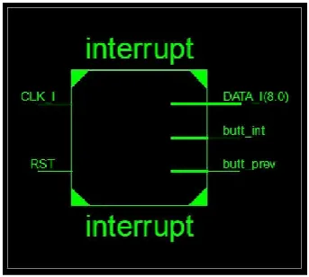
Simulation results of Interrupt controller
Fig. 15. Top view of Interrupt controller
[image:4.595.346.522.478.606.2]Fig. 16. RTL view of Interrupt controller
Fig. 17. Timing diagaram of Interrupt controller
[image:4.595.45.282.482.788.2] [image:4.595.309.561.638.736.2]Conclusion
The present paper deals with the design of FPGA based 8 bit RISC processor with peripherals. The basic modules of this processor are programmed by using Verilog Hardware Description Language (VHDL), it is then verified the simulation result using XILLINX ISE 12.4 tool. The present 8
bit ALU performs arithmetic and logical operations such as
AND, OR, NOT, NOP, NAND, NOR, XOR etc. Furthermore, ALU contains logic gates, adder, substractor, multiplexers etc for the intended operation. In the nutshell, the designed ALU performs its intended operations. It has the peripherals such as SPI, UART, Timer/Counter, and PWM and interrupt controller which performs several external operations.
REFERENCES
Kulkarni, S. V. 2016. A. I. Nadaf, P. P. Shah. M. K. Bhanrkar, Design of FPGA based 8 bit RISC Processor, International
journal of VLSI design and Embedded system, Vol 7, Jun
1691-1698.
Uma, R. 2012. Design and Performance analysis of 8 bit RISC processor using Xilinx Tool., International Journal Of
Engineering Research and Applications, vol 2 , issue 2,
Mar 2012, 053-058.
Luker, Jarrod D., Prasad, Vinod B. 2001 “RISC system design in a FPGA” MWSCAS 2001, vol2,2001, pp. 532-536, Mishra K. K., Purwar R., Singh P., “International Journal of
Electronics and Communication” vol3,January 2015, PP 35-42,
Chokkalingam. S, Arunprasath. V., Dineshkumar. P, Implementation of 8 bit microcontroller using VLSI, International Journal of Advanced Research in Computer
science and technology, Vol. 2 Issue 1, Jan-Mar 2014,
221-224