Simulation and analysis of 21 level multilevel
inverter using PD, POD, APOD and VF PWM
techniques.
Usha M S1, T N Raghavendra2
PG Student [Power Electronics], Dept. of EEE, UVCE, Bengaluru, Karnataka, India1
Assistant Professor [Power Electronics], Dept. of EEE, UVCE, Bengaluru, Karnataka, India2
ABSTRACT: Multi-level inverter technology has emerged as a very important alternative in the area of high-power medium voltage energy control. Two level inverters are those which creates a voltage or a current with levels either 0 or ±V dc. To achieve an eminence output voltage or a current waveform with a lowest amount of ripple content, they need high switching frequency. When working at high frequency, high power and high voltage applications these two level inverters have a few restrictions. The multi-level inverter is to produce a quasi sinusoidal voltage from many levels of dc voltages. The obtained output waveform has more steps, which creates a staircase wave form that reaches to a preferred wave form, as the number of levels increases.
KEYWORDS: Multilevel inverter, PO, POD, APOD, VF PWM techniques, THD.
I.INTRODUCTION
In recent years, multi-level inverter has drawn a great attention in industry, due to use in high power and high voltage application. A group of DC sources and switching devices together constitute a multi level inverter, the output of which is a stepped waveform with number of DC levels. Many topologies with wide variety of control techniques are developed in the past few decades. The conventional multi level inverters like Neutral Point Clamped or Diode Clamped (NPC), the Flying Capacitor (FC), and the Cascaded H-Bridge (CHB) have some drawbacks. Hence a wide research is going on to develop Smart multilevel inverters with huge advantages. NPC uses large number of clamping diodes with deviating voltages; in FC switching utilization is poor with large number of capacitors and unbalanced DC link voltage is the main drawback of this topology. But cascaded H-Bridge gives a better output THD and less distortion compared to NPC and FC topologies but it requires large number of dc due to increase in number of voltage levels circuit become complex, efficiency and reliability may be reduced
.
This paper presents a new multilevel inverter topology using H-bridge which is implemented in single-phase with less count of switches and gate drive circuit. This paper present 21-level multilevel inverter with different PWM technique which is used for controlling the output voltage within inverter i.e Phase disposition pulse width modulation (PD PWM), Phase opposition disposition pulse width modulation (POD PWM), Alternate phase opposition disposition pulse width modulation (APOD PWM), Variable frequency pulse width modulation (VF PWM). This new multilevel inverter topology as less number of switches diode as other conventional multilevel inverter.The circuits are simulated in a MATLAB/Simulink environment and the results are verified.
II.LITERATURE SURVEY
increase.
The objective of reduced switch MLI topology is to increase number of levels with less
number of switches and sources. This topology reduces the total harmonic distortion, lowers the
electromagnetic interference and produces high voltage.
TABLE 1- COMPARISON OF DIFFERENT TOPOLOGIES
III.METHODOLOGY
MULTI CARRIER PULSE WIDTH MODULATION TECHNIQUE
The proposed asymmetric MLI is performed using multicarrier modulation techniques. Carriers used in MLI may be vertically shifted or horizontally shifted. The general principle of a carrier based PWM is the comparison of a reference waveform with a carrier waveform, this typically being a triangular waveform. The carrier frequency defines the switching frequency of the converter and the high order harmonic component of the output voltage. Sub harmonic PWM is otherwise known as sinusoidal PWM (SPWM). The reference waveform has the amplitude Am and frequency fm and it is centered above the zero level. The reference wave is continuously compared with each of the carrier signals. If the reference wave is greater than a carrier signal, then the active device corresponding to the carrier are switched on. Otherwise the devices switch off. The frequency ratio mf is defined as mf=fc/fm. The amplitude modulation index ma is defined as ma=2Am/ (m-1) Ac.
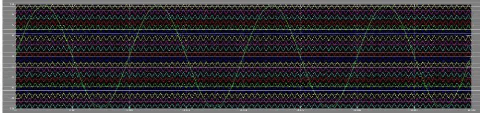
A)Phase disposition pulse width modulation (PD PWM):-
B)Phase opposition disposition pulse width modulation (POD PWM):-
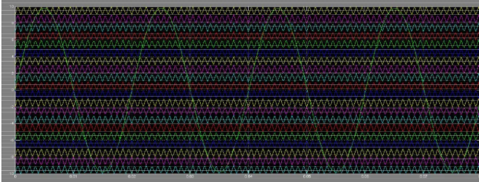
In POD PWM strategy all (m-1) carriers signal are in same phase to each other above the zero-axis with same amplitude and frequency but carrier wave below zero-axis is 1800 out of phase to above zero-axis carrier waveform. The reference wave is continuously compared with each of the carrier wave, if the amplitude of the reference wave is greater than the carrier wave pulse will be generated. The carrier arrangement for this technique is shown in fig.2
Fig.2 Carrier arrangement for PODPWM strategy.
C)Alternate phase opposition disposition pulse width modulation (APOD PWM):-
In APOD PWM strategy all the carrier wave is out of phase with its neighboring carrier wave by 1800 but all carriers has same amplitude and frequency. The reference wave is continuously compared with each of the carrier wave, if the amplitude of the reference wave is greater than the carrier wave pulse will be generated. The carrier arrangement for this technique is shown in fig.3
D)Variable Frequency PWM (VF PWM):-
In VF PWM all the carrier wave has variable frequency with each other. The reference wave is continuously compared with each of the carrier wave, if the amplitude of the reference wave is greater than the carrier wave pulse will be generated. The carrier arrangement for this technique is shown in fig.4
Fig.4 Carrier arrangement for VFPWM strategy.
IV.PROPOSED TECHNOLOGY
Twenty one level asymmetrical multilevel inverter consists of one cell of H-bridge with four main switches, four auxiliary switches and four diodes. It has four separate DC sources dc sources for 21 level MLI. The new proposed topology operates in different switching modes and it is given in table 2 For H-bridge having four switches S1, S2, S3 and S4 in which one pair of switches working for positive half cycle i.e switch S1 and S2 and other pair of switch working for negative half cycle i.e switch S3 and S4 with four separate dc sources Vdc, 2Vdc, 3Vdc and 4Vdc. There are twenty one modes of operation for this topology in order to generate 21 level output.
V. SIMULATION RESULTS AND DISCUSSIONS
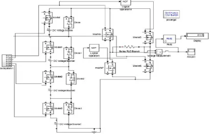
The twenty one level new hybrid multilevel inverter circuit was simulated in Matlab/Simulink Environment and the results were analysed for a Resistive load. And the simulation circuit is as shown in fig. 6
Fig. 6 Simulation Circuit of 21 Level Inverter with Resistive load
Fig 7 shows the output voltage waveform and FFT analysis of 21 level multilevel inverter using Phase disposition pulse width modulation ( PD PWM) technique. Total harmonic distortion(THD) is about 6.09% using MATLAB simulink.
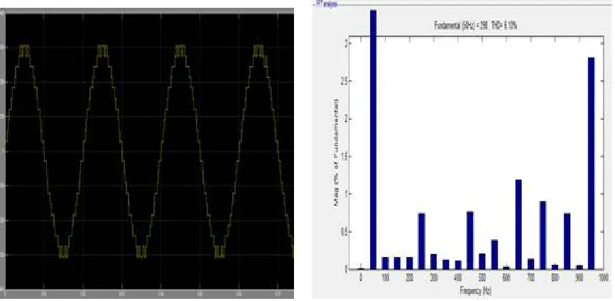
Fig 8 Simulated output voltage waveform and FFT analysis of 21 level MLI using PODPWM
Fig 8 shows the simulated output voltage waveform and FFT analysis of 21 level multilevel inverter using Phase opposition disposition pulse width modulation (POD PWM) technique. Total harmonic distortion(THD) is about 6.13% using MATLAB simulink.
Fig 9 Simulated output voltage waveform and FFT analysis of 21 level MLI using APODPWM
Fig 10 Simulated output voltage waveform and FFT analysis of 21 level MLI using VFPWM
Fig 10 shows the simulated output voltage waveform and FFT analysis of 21 level multilevel inverter using variable frequency pulse width modulation (VF PWM) technique.Total harmonic distortion(THD) is about 5.40% using MATLAB simulink.
VI.CONCLUSION
A new 21 level multilevel inverter with multicarrier pulse width modulation technique i.e Phase Disposition PWM (PDPWM), Phase Opposition Disposition PWM (PODPWM), Alternate phase opposition disposition pulse width modulation (APOD PWM) and Variable Frequency PWM (VF PWM) has been presented in this paper. This topology gives a total harmonic distortion of 6.09% , 6.13%, 6.24% and 5.40% respectively and the ac output voltage waveform almost resembles a sine wave. By comparing all the four techniques we can say that VFPWM is more advantageous because of lesser THD than other three techniques. This helped in reducing the switching losses by a great extent. The emphasis can be on eliminating the spikes which can appear in the output voltage waveform.
REFERENCES
[1]Muhammad H Rashid , "Power Electronics: circuits, Devices and Applications", Pearson Education, Third Edition, 2004.
[2] J.S. Lai and F.Z. Peng, "Multilevel Converters - A new breed of power converters," Conference Record of the IEEE-lAS Annual Meeting, 1995, pp. 234S-2356.
[3] M. Manjrekar and G. Venkataramanan, "Advanced topologies and modulation strategies for multilevel inverters," Conference Record of the IEEE-PESC, 1996, pp. 1013-10IS.
[4] J. Rodriguez, J.-S. Lai, and F. Z. Peng, "Multilevel inverters: a survey of topologies, controls, and applications," IEEE Trans. Ind. Electron., vol. 49, pp. 724 -73S, 2002.
[5] Franquelo LG, Rodriguez JL, Leon J, Kouro S, Portillo R, Prats MA. The age of multilevel converters arrives. IEEE Ind Electron. Mag 2008;2(2):28–39.IEEE Transactions on Industrial Electronics, vo1.56,Nol.,January 2009.
[6] E brahimBabaei, Ali Dehqan, Mehran Sabahi A new topology for multilevel inverter considering its optimal structures, Electric Power Systems Research103 (2013) 145– 156.
[7] E. Babaei, Optimal topologies for cascaded sub-multilevel converters, J. PowerElectron. 10 (3) (2010) 251–261.
[8] Nabae A, Takahashi I, Akagim H. A new neutral point clamped PWM inverter.IEEE Trans Ind Appl 1981;IA-17(5):518–23. [9] S. Gui-Jia, Multilevel dc-link inverter, IEEE Trans. Ind. Appl. 41 (3) (2005), 848–845.
[10]A. Radan, A. H. Shahirinia, and M. Falahi, “Evaluation of carrier based PWM methods for multi-level inverters,” in Proc. IEEE ISIE, 2007, pp. 389–394.