This is a repository copy of Compact half-mode substrate integrated waveguide bandpass
filters with capacitively loaded complementary single split ring resonators.
White Rose Research Online URL for this paper:
http://eprints.whiterose.ac.uk/82363/
Version: Accepted Version
Article:
Huang, L, Robertson, ID and Yuan, N (2013) Compact half-mode substrate integrated
waveguide bandpass filters with capacitively loaded complementary single split ring
resonators. Microwave and Optical Technology Letters, 55 (7). 1602 - 1606. ISSN
0895-2477
https://doi.org/10.1002/mop.27604
[email protected] https://eprints.whiterose.ac.uk/ Reuse
Unless indicated otherwise, fulltext items are protected by copyright with all rights reserved. The copyright exception in section 29 of the Copyright, Designs and Patents Act 1988 allows the making of a single copy solely for the purpose of non-commercial research or private study within the limits of fair dealing. The publisher or other rights-holder may allow further reproduction and re-use of this version - refer to the White Rose Research Online record for this item. Where records identify the publisher as the copyright holder, users can verify any specific terms of use on the publisher’s website.
Takedown
If you consider content in White Rose Research Online to be in breach of UK law, please notify us by
COMPACT HALF-MODE SUBSTRATE
INTEGRATED WAVEGUIDE BANDPASS
FILTERS WITH CAPACITIVELY-LOADED
COMPLEMENTARY SINGLE SPLIT RING
RESONATORS
Liwen Huang1, Ian. D. Robertson1 and Naichang Yuan2 1Institute of Microwaves and Photonics, University of Leeds, Leeds, LS2 9JT, United Kingdom; Corresponding author: [email protected]
2Microwave Research Centre, National University of Defense Technology, Hunan, 410073, China
ABSTRACT: A novel compact half-mode substrate integrated waveguide (HMSIW) filter with modified complementary single split ring resonators (CSSRRs) is presented in this letter. It is shown that the proposed structure demonstrates lower resonant frequency and enhanced miniaturization compared to the HMSIW with conventional CSSRRs due to the additional capacitance generated by an additional conductor connected to the inner metal disk and overlaid across the ground plane of the CSSRR. Even lower resonant frequency and greater miniaturization can be achieved conveniently by increasing the area of the overlap or using thin dielectric substrate and the technique can readily be realized in a range of multilayer technologies. The equivalent circuit model for the proposed element is derived and a second order bandpass filter with the proposed element, operating at 4.92 GHz, is designed and fabricated. Excellent agreement is achieved between the simulation and the measurement. The proposed HMSIW filter shows good selectivity, low loss and compact size, with the total size without the feed lines being only 9.8 mm × 7mm (0.17 0 × 0.115 0).
Key words: complementary single split ring resonator (CSSRR); half-mode substrate integrated waveguide
(HMSIW); microwave filters; bandpass filters;
miniaturization
1. INTRODUCTION
The rapid growth of modern wireless communication system has increased the demand for compact microwave filters with high performance. Recently, the complementary split ring resonator (CSRR) [1] has attracted a great deal of interest in the microwave filter design due to its favorable characteristics such as the high Q factor and compact size. The CSRR is the negative image of the split ring resonator (SRR) [2]. It is capable of generating negative effective permittivity and can be modeled as a resonant LC tank driven by external electric fields. Its applications in the design of compact filters such as microstrip filters and coplanar waveguide filters have been illustrated in [3-4]. Moreover, the combination of the substrate integrated waveguide (SIW) [5] and the CSRR, which could lead to the passband below the cutoff frequency of the SIW, has also been applied into the design of the SIW filters with reduced size [6-7].
Meanwhile, the half-mode substrate integrated waveguide (HMSIW) [8], which is nearly half the size of the conventional SIW, while keeping the advantages of compact size, low loss and high Q factor, is also quite popular. The application of the CSRR to the design of compact HMSIW filters with high performance has been reported in [9-10].
The complementary single split ring resonator (CSSRR) has similar properties to the CSRR. It can be modeled as the LC resonant tank excited by proper electric fields [11]. Its applications to the design of microwave filter have been illustrated in [11]. In this letter, by adding an overlap region between the inner metal disk and the ground plane of the CSSRR, it is shown that the modified CSSRR has enhanced capacitance, lower resonant frequency and greater miniaturization. The proposed structure is applied to the design of a compact HMSIW bandpass filter. Even lower frequency can be obtained conveniently by increasing the area of the overlap region or using thin dielectric substrate, with the total size unchanged. The equivalent circuit model is derived and used to design a bandpass filter. The simulated and measured results agree well. The proposed filter is compact, low loss and shows good selectivity. Thus, it has a great potential in the design of miniaturized microwave systems.
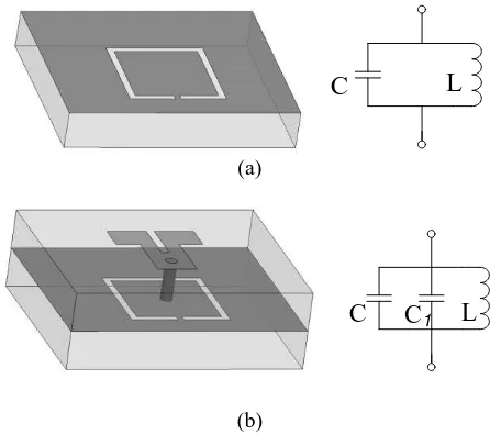
2. CONFIGURATION OF THE MODIFIED CSSRR Figure 1(a) shows the configuration of the conventional CSSRR and its equivalent circuit model. It can be modeled as an LC resonant tank driven by external electric fields [11]. As shown in Figure 1(a), L represents the total inductance of the CSSRR, and C is the total capacitance. The configuration of the modified CSSRR is presented in Figure 1(b). It consists of two layers. The lower layer is the conventional CSSRR. On the top surface, a conductor layer which overlaps the ground plane of the CSSRR is connected to the centre of the inner metal disk of the CSSRR through a metalized via. Compared to the conventional CSSRR, the modified CSSRR is capable of achieving lower resonant frequency as additional capacitance is obtained. The simplified equivalent circuit model for the modified structure is shown in Figure 1(b), where L stands for the total inductance of the modified CSSRR; C represents the slot capacitance between the inner metal disk and the ground plane of the CSSRR and C1 represents the additional capacitance between the extra conductor and the ground plane of the CSSRR.
L
C
(a)C
1C
L
(b) [image:2.595.322.545.551.749.2]3. CONFIGURATION OF THE HMSIW WITH THE MODIFIED CSSRR
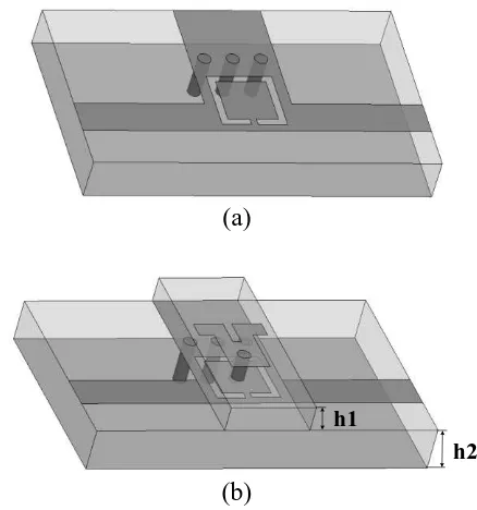
Figure 2(a) shows the configuration of the HMSIW with the conventional CSSRR. The CSSRR is etched on the top broadwall of the HMSIW. The microstrip feed line is employed to excite the HMSIW with the CSSRR. Since the CSSRR requires axial electric excitation and the electric field of the main mode of the HMSIW is perpendicular to the top and bottom broadwalls, it guarantees that the CSSRR is properly excited. Based on this configuration, the element of the HMSIW with the modified CSSRR is proposed. As shown in Figure 2(b), an extra layer is added which is used to enhance the total capacitance of the CSSRR by having a conductor that is connected to the centre of the inner metal disk of the CSSRR through a metal via and overlaps the ground plane.
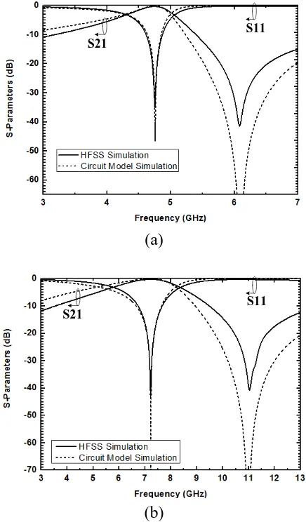
A prototype of the proposed element has been designed with the HFSSTM and fabricated on the Rogers RO 4350 with the dielectric constant r being 3.48. Figure 3 shows the photograph and layout of the proposed element. The parameters are as follows: h1 = 0.8 mm, h2 = 0.3 mm, b = 3 mm, g = 0.3mm, d = 0.34 mm, t = 0.4 mm, w = 4.5 mm, s =1.68 mm, l = 0.4 mm, dr = 1.1 mm, ds = 1.9 mm, wt = 0.4 mm, ws = 0.8 mm, wc = 1.4 mm, wy = 1.8 mm, wx = 2.3 mm. The simulated and measured frequency responses are shown in Figure 4. It can be seen that measured resonant frequency is 4.87 GHz, with a transmission zero introduced at 6.09 GHz. Good agreement has been achieved between the simulation and the measurement. For comparison, the element of the HMSIW with the conventional CSSRR (see Figure 2(a)) with the dimensions identical to the lower layer of the HMSIW with the modified CSSRR was also studied. The simulated responses are plotted in Figure 4, compared with that of the modified element. It can be seen that the resonant frequency of the HMSIW with the conventional CSSRR is 7.23 GHz, which is much higher than that of the modified structure.
To better understand the response of the proposed element, the simplified equivalent circuit model has been derived. As shown in Figure 5, the metallic vias forming the HMSIW is modelled as Lv; the modified CSSRR is modelled as the resonant tank with the inductance Ls and the capacitance Cs; the magnetic coupling between the HMSIW and the modified CCSRR is represented by Lc. It is mainly through the split of the ring between the HMSIW and the CSSRR. The capacitive coupling is denoted by Cc, and it is mainly through the slot coupling between the HMSIW and the CSSRR. Moreover, this equivalent circuit model can also be applied to the element of the HMSIW with the conventional CSSRR (see Figure 2(a)). In this case, Lv represents the metal vias forming the HMSIW; Ls and Cs stand for the total inductance and capacitance of the conventional CSSRR, respectively; Lc and Cc represent the inductive and capacitive coupling between the HMSIW and the CSSRR, respectively. From the circuit model, it can be seen that a transmission zero is generated:
1
2 fz
L Cs s
The simulated results of the proposed element and the HMSIW with the conventional CSSRR from the equivalent circuit model are shown in Figure 6(a) and Figure 6(b), respectively, compared with that from the HFSSTM. Excellent agreement has been obtained. For the proposed structure, the parameters of the circuit model are: Lv = 2.5 nH, Lc = 0.91
nH, Cc = 0.75 pF, Ls = 1.68 nH, Cs = 1.3 pF; for the case of
the HMSIW with conventional CSRRs, the parameters are:
Lv = 2.4 nH, Lc = 0.6 nH, Cc = 0.35 pF, Ls = 1.755 nH, Cm =
0.753 pF. By comparing the value of the lumped element of the circuit model, it can be seen that the modified structure has larger capacitance, denoted by Cs, which further verifies that enhanced capacitance is obtained.
The loading capacitance can be tuned conveniently by changing the layout of the conductor and the dielectric substrate parameters. Figure 7 presents the simulated results with different thickness of the upper layer, h2. It can be seen that the resonant frequency reduces significantly when h2 becomes smaller, due to the increase of the capacitance between the conductor and the ground plane of the CSSRR. This indicates that even more compact sizes can be achieved conveniently by using thin dielectric substrate for the upper layer. Moreover, a smaller size of the proposed element can also be achieved by increasing the length and the width of the conductor overlap appropriately.
(a)
h1
h2
(b)
[image:3.595.327.546.374.608.2](a)
w
ds
dr
l
s
g
d
b
wt
wy
ws
wc
wx
(b)
(c)
Figure 3 (a) Photograph of the fabricated element. (b) Layout of the lower layer of the proposed element. (c) Layout of the upper layer of the proposed element. Grey shading represents the metallization
S11
S21
Figure 4 Simulated and measured results of the proposed element, compared with the HMSIW with the conventional CSSRR
Port 1
L
cL
cPort 2
L
vL
vL
sC
s [image:4.595.326.544.38.410.2]C
cC
cFigure 5 Equivalent circuit model of the proposed element
S11 S21
(a)
S11 S21
(b)
[image:4.595.58.261.39.200.2]Figure 6 (a) Circuit model simulation of the proposed element. (b) Circuit model simulation of the HMSIW with the conventional CSSRR
Figure 7 Simulated frequency responses with different thickness of the dielectric substrate of the upper layer, h2
4. HMSIW BANDPASS FILTER WITH THE PROPOSED STRUCTURE
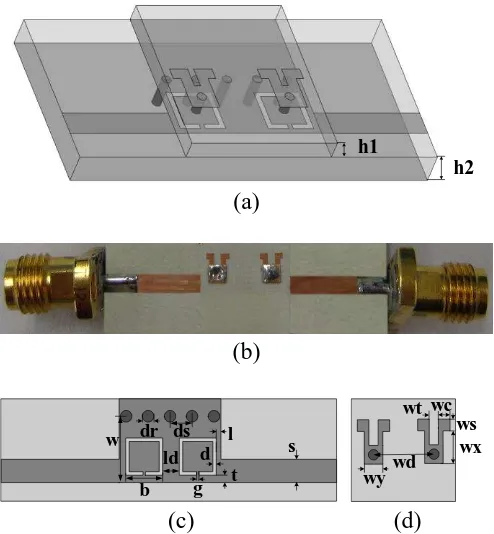
[image:4.595.38.281.258.438.2] [image:4.595.325.544.454.619.2] [image:4.595.38.246.523.603.2]mm, g = 0.3mm, d = 0.34 mm, t = 0.5 mm, w = 4.5 mm, s =1.68 mm, l = 0.4 mm, dr = 1.1 mm, ds = 2 mm, ld = 2.6 mm, wt = 0.4 mm, ws = 0.8 mm, wc = 2.2 mm, wy = 1.8 mm, wd = 5.6 mm, wx = 2.4 mm. The simulated results with HFSSTM and the measured transmission responses are shown in Figure 9. It can be seen that the measurement agrees well with the simulation. The measured centre frequency and 3 dB bandwidth are 4.92 and 0.6 GHz, respectively. The measured insertion loss is 0.8 dB including the feed lines and SMA connectors. The measured in-band return loss is better than 20 dB. The total size of the filter without the feed line is only 9.8 mm × 7mm (0.17 0 × 0.115 0), which is very compact.
h1 h2
(a)
(b)
w ld s ds dr t l g d bws wd wt wy wc wx
(c)
(d)
Figure 8 (a) Configuration of the proposed filter. (b) Photograph of the fabricated filter. (c) Layout of the upper layer of the filter. (d) Layout of the lower layer of the filter. Grey shading represents the metallization
S11
S21
Figure 9 Simulated and measured transmission responses of the proposed bandpass filter
5. CONCLUSIONS
A novel compact half-mode substrate integrated waveguide (HMSIW) filter with a capacitively-loaded complementary single split ring resonator (CSSRR) is presented in this letter. The element of the HMSIW with modified CSSRRs is investigated. The proposed element demonstrates lower resonant frequency and greater miniaturization compared to the HMSIW with the conventional CSSRR, due to the additional capacitance introduced by the extra conductor layer overlapping the inner metal disk and the ground plane of the CSSRR. Even larger capacitance and lower frequency can be achieved conveniently by increasing the overlap area or decreasing the thickness of the dielectric substrate. The equivalent circuit model of the proposed element has been derived. A second order bandpass filter with the proposed element, with the center frequency at 4.92 GHz, has also been designed and fabricated. The measurement agrees well with the simulation. The proposed filter has the advantages of quite compact size, low losses and good selectivity. The total size of the filter without the feed line is only 9.8 mm × 7mm (0.17 0 × 0.115 0). Therefore, it has greatly potential in the design of microwave system where a small size is critical.
ACKNOWLEDGMENTS
The authors wish to acknowledge Weiwei Wu in Changsha, China, for fabricating the filters. The financial support received from University of Leeds-China Scholarship Council program is gratefully acknowledged.
References
1. F. Falcone, T. Lopetegi, J. D. Baena, R. Marqués, F.
Martín, and M. Sorolla, Effective negative-epsilon stopband microstrip lines based on complementary split ring resonators, IEEE Microw Wireless Compon Lett 14 (2004), 280-282.
2. J. B. Pendry, A. J. Holden, D. J. Robbins, and W. J.
Stewart, Magnetism from conductors and enhanced nonlinear phenomena, IEEE Trans Microwave Theory & Tech 47 (1999), 2075-2084.
3. Y. Yang; Z. Xi and N. C. Karmakar, Microstrip lowpass
filter based on split ring and complementary split ring resonators, Microwave Opt Technol Lett 54 (2012), 1723-1726.
4. I. Gila, M. Moratab, R. Fernándeza, X. Rottenbergc and
W. De Raedtc, Characterization and modelling of switchable stop-band filters based on RF-MEMS and complementary split ring resonators, Microelectronic Eng 88 (2011), 1-5.
5. D. Deslandes, and Ke Wu, Single-substrate integration technique of planar circuits and waveguide filters, IEEE Trans Microwave Theory & Tech 51 (2003), 593 – 596.
6. K. Deng, Z. Guo, C. Li and W. Che, A compact planar
bandpass filter with wide out-of-band rejection implemented by substrate-integrated waveguide and complementary split-ring resonator, Microwave Opt Technol Lett 53 (2011), 1483-1487.
7. L. Zhou, S. Liu, N. Gao, Y. Chen and Y. Wei,
Miniaturized substrate integrated waveguide filter with complementary spiral resonator, Microwave Opt Technol Lett 53 (2011), 1308-1311.
8. W. Hong, B. Liu, Y. Wang, Q. Lai, H. Tang, X. X. Yin,
[image:5.595.36.283.200.467.2] [image:5.595.46.274.522.696.2]microwave and millimeter wave application, Proc Joint 31st Int Conf Infrared Millimeter Waves 14th Int Conf Terahertz Electronics, Shanghai, Peoples R. China, 2006, pp. 219.
9. L. Qiang, H.-M. Lu, W. Zhao, H.-B. Qin and B. Liu, Half mode substrate integrated waveguide miniaturization using complementary split ring resonators, Microwave Opt. Technol. Lett., 53 (2011), 1074-1077.
10. L. Qiang, Y.-J. Zhao, Q. Sun, W. Zhao, and B. Liu, A compact UWB HMSIW bandpass filter based on complementary split-ring resonators, Prog. Electromagn. Res. C, 11 (2009), 237-243.