LOW POWER CONSUMPTION CMOS DESIGN
Ms. Shivani Gupta
Electronics and Communication Engineering Dronacharya College of Engineering,
Gurgaon, India
Ms. Suman
Electronics and Communication Engineering Dronacharya College of Engineering,
Gurgaon, India [email protected]
Ms. Sonal Aggarwal
Electronics and Communication Engineering Dronacharya College of Engineering,
Gurgaon, India [email protected]
ABSTRACT
It has many applications in sensor interfaces and biomedical signal processing units. Biomedical signals are usually of 10-mHz to 100-Hz frequency range. The performance of filters designed by the use of passive components degrades at audio frequencies and the required resistances and inductances values calculated from the mathematical expression are very difficult to meet from the market. To find a solution to this problem is a study to realize Passive Filters into Active Filters using Operational Transconductance.
Index Terms sensors, filter, OTA, power consumption.
I.INTRODUCTION
An electrical filter is "filter-out" unwanted signals and an ideal filter will separate and pass sinusoidal input signals based upon their frequency. Filters are networks that process signals in a frequency-dependent manner. The basic concept of a filter can be explained by examining the frequency dependent nature of the impedance of capacitors and inductance.[3]It have many practical applications. A simple, single pole, low-pass filter (the integrator) is often used to stabilize amplifiers by rolling off the gain at higher frequencies where excessive phase shift may cause oscillations.[5] A simple, single pole, high pass filter can be used to block DC offset in high gain amplifiers or single supply circuits. Filters can be used to separate signals, passing those of interset and unwanted frequencies.
II. TYPESOFFILTER
FILTERS CAN BE DIVIDED INTO TWO DISTINCT WAYS:
A. Active filters B. Passive filters.
have no signal gain, therefore their output level is always less than the input. Based on frequency of signals they allow to pass through them, filters can be divided into following categories.
[image:2.595.254.342.164.261.2]A. Low Pass Filter:
Fig 1.1 Low pass filter
There are Low-pass filters that allow only low frequency signals to pass where fc is cut off frequency.
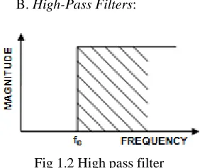
[image:2.595.244.385.307.426.2]B. High-Pass Filters:
Fig 1.2 High pass filter
High-pass filters that allow only high frequency signals to pass through.
C. Band-Pass Filters
Fig 1.3 Band pass filter
D. Band Reject Filter:
A complement to the band pass filter is the band reject, or notch filter. Here, the pass bands include frequencies below f l (lower cut-off frequency) and above f h (upper cut-off frequency) .The band from f l to f h is in the stop-band.
It allow signals falling within a certain frequency range to pass through. If a high-pass transfer function can be realized using a Cauer 1-form. The kth element is given by: filter and a low-pass filter are cascaded, a band pass filter is created. The band pass filter passes a band of frequencies between a lower cut-off frequency, f l, and an upper cut-off frequency, f h. Frequencies below f l and above f h are in the stop-band.
III. FILTERPARAMETERS
The idealized filter unfortunately, cannot be easily built. The transition from pass band to stop-band will not be instantaneous, but instead there will be a transition region. Stop band attenuation will not be infinite.
IV. FILTERTOPOLOGIES
Two main topologies are available to implement a linear analog filter.
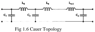
[image:3.595.219.414.506.573.2]A. CAUER TOPOLOGY
Fig 1.6 Cauer Topology
B. SALLEN-KEY TOPOLOGY
Fig 1.7 Sallen Key Topology
The Sallen-Key topology uses active and passive components (operational amplifiers, resistors and capacitors) to implement a linear analog filter.
V.OTABASEDLOW-PASSFILTERS
The conventional operational amplifier (op-amp) is used as the active device in the vast majority of the active filter literature. A host of practical filter designs have evolved following this approach.[4] It has also become apparent, however, that operational amplifier limitations preclude the use of these filters at high frequencies, attempts to integrate these filters have been unsuccessful (with the exception of a few no demanding applications), and convenient voltage or current control schemes for externally adjusting the filter characteristics do not exist.[6] In this case basic first, second and higher-order structures using the transconductance amplifier .
VI.OTA MODEL
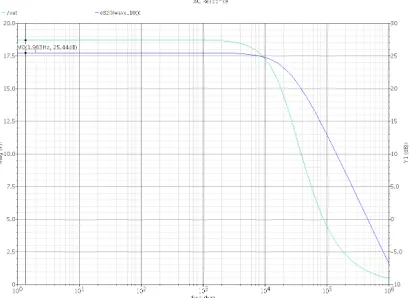
[image:4.595.193.398.573.722.2]The transconductance gain, gm, is assumed proportional to Ib. The proportionality constant h is dependent upon temperature, device geometry, and the process.
This OTA is designed for 5µW and 25 dB with 1.8 V power supply in 0.18µm UMC technology.[10] Then following characteristic has been obtained shown in Fig where Obtained Gain is 25.44dB and power consumed is 4.88µW of above differential OTA.
VII.BALANCED DIFFERENTIAL OTA
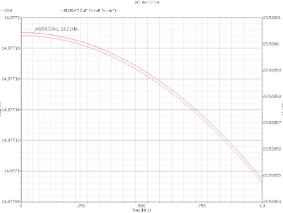
[image:5.595.201.403.232.384.2]In a balanced OTA there are three current mirrors and a single output. The complexity of differential OTA structures is also provide an improvement in offset reduction and robustness, but not necessarily with an improvement for high-frequency applications. Thus trade-offs between speed and accuracy should be established for each particular application.
Fig 1.9 Gain characteristic of balanced OTA
VIII.APPLICATIONS
A. Typical data acquisition system for Signal is shown in fig. The preamplifier must amplify the input signal to a higher level with low distortion and low noise.
Fig1.10 Block diagram of a general purpose bioelectric signal acquisition system
B. Filters have many practical applications. A simple, single pole, low-pass filter (the integrator) is often used to stabilize amplifiers by rolling off the gain at higher frequencies where excessive phase shift may cause oscillations.
C. A simple, single pole, high-pass filter can be used to block DC offset in high gain amplifiers or single supply circuits. Filters can be used to separate signals, passing those of interest, and attenuating the unwanted frequencies.
D. In integrated wireless receivers.
E. The electrical activity within living organisms,.
F. Butterworth low pass filter for aerospace extreme environment applications is implemented in SiGe BiCMOS technology. G. COGNITIVE radio
CONCLUSION
FUTURESCOPE
This work can be extended to designing of low pass filter with low frequency and low power in the future. However, the basic need in order to design low pass filter for low power is to minimize the power of OTA.
REFERENCES
[1].Chun-Lung Hsu, Mean-Hom Ho, Yu-Kuan Wu and Ting-Hsuan Chen, “Design of Low-Frequency Low-Pass Filters for Biomedical Applications, ” IEEE, Circuits and Systems, pp. 690-695 ,December2006 .
[2]. Esther Rodriguez Villegas, Alexander J. Casson and Phil Corbishley, “A Subhertz Nanopower Low-Pass Filter, ” IEEE Circuits And Systems, vol .58, no.6, June 2011.
[3]. Haidong Liu, Xiaohong Peng and Wuchen Wu, “Design of a Gm-C Low Pass Filter with Low Cutoff frequency.” IEEE Microelectronics & Electronics , pp. 125-128 , January 2009.
[4]. Prasant K. Mahapatra, Manjeet Singh , Neelesh Kumar , “Realization of active filters using operational transconductance amplifier (OTA)”, Journal of the Instrument Society of India, pp 1-9.
[5]. Randall L. Geiger , Edgar Sánchez-Sinencio “Active Filter Design Using Operational Transconductance Amplifiers: A Tutorial,” IEEE Circuits and Devices Magazine, vol. 1, pp.20-32, March 1985.
[6]. F. Krummenacher, "High-Voltage Gain CMOS OTA for Micropower SC Filters," IEEE Electron. Letters, vol. 17, pp. 160-162, February 1981.
[7]. Rezzi, F., A. Bashirotto and R. Castello, “ A 3V 12- 55 MHz BiCMOS Pseudo - Differential Continuous- Time Filter”, IEEE Circuits and System I, vol. 42, pp. 896-903, November 1995.
[8]. Andras Timar and Marta Rencz , “Design issues of a low frequency low-pass filter for medical applications using CMOS technology,” IEEE, Design and Diagnostics of Electronic Circuits and Systems, pp.1-4, April 2007
[9]. S S-Bustos, J S Martinez , F Maloberti and E Sanchez-Sinencio, “A 60-dB Dynamic-Range CMOS Sixth-Order 2.4-Hz Low-Pass Filter for Medical Applications”, IEEE Transactions On Circuits And Systems, vol. 47, pp. 1391-1398, no.12, December 2000.
[10]. Tien-Yu Lo and C Chih Hung, “A 1-V Gm-C Low-Pass Filter for UWB Wireless Application”, IEEE Solid-State Circuits,pp.277-280, November 2008 .