University of South Carolina
Scholar Commons
Theses and Dissertations
1-1-2013
Impedance Estimation Using Randomized Pulse
Width Modulation and Power Converters
William M. McCoy
University of South Carolina
Follow this and additional works at:https://scholarcommons.sc.edu/etd Part of theElectrical and Electronics Commons
This Open Access Thesis is brought to you by Scholar Commons. It has been accepted for inclusion in Theses and Dissertations by an authorized administrator of Scholar Commons. For more information, please [email protected].
Recommended Citation
I
MPEDANCEE
STIMATIONU
SINGR
ANDOMIZEDP
ULSEW
IDTHM
ODULATION ANDP
OWERC
ONVERTERSby
Matthew McCoy
Bachelors of Science
University of South Carolina, 2013
Submitted in Partial Fulfillment of the Requirements
For the Degree of Masters of Science in
Electrical Engineering
College of Engineering and Computing
University of South Carolina
2013
Accepted by:
Herbert Ginn III, Major Professor
Roger Dougal, Committee Member
© Copyright by Matthew McCoy, 2013
A
CKNOWLEDGEMENTSI would like to thank my advisor Dr. Herbert Ginn III for his leadership
throughout my graduate studies. I also appreciate the efforts of my committee member
Dr. Roger Dougal, as well as the rest of my graduate and undergraduate professors.
Special thanks are also extended to my friends, family, and David Metts for their support
A
BSTRACTWith the adoption of technologies such as alternative energy production, DC
power grids, and electric vehicles, the use of high power switching converters has seen a
dramatic increase. These power converters serve many rolls such as grid-tied inverters in
solar farms, high power charging for electric vehicles, motor drives for industrial
applications, and DC links in transmission systems. With the increased prevalence of
such devices, it is only natural to attempt to optimize their operation. As with any level of
converter, it is desirable to have accurate control over the generated voltages and
currents. Often, these controllers implement some form of predictive control which
requires knowledge of system parameter values to operate properly. Due to several
factors, including temperature and component non-linearity, these component values can
vary during normal operation. This can lead to degradation of closed loop control and
system instabilities. If one is able to measure system parameters while the converter is
operating, control parameters can be updated in real time to optimize the system
performance.
A significant percentage of the size and cost of switching converters are filter
elements meant to reduce the amount of noise injected into other attached circuits, or in
the case of grid-tied converters, noise injected into the grid. As power levels increase, the
size, cost, and power lost in the filter becomes greater. To minimize these negative
smaller filter elements. One such technique is Randomized Pulse Width Modulation
which removes the large harmonic spikes present in standard switching systems, and
replaces them with a wide frequency energy spectrum.
The objective of this research is to examine the feasibility of online impedance
identification by combining and modifying existing technologies. Specifically,
Randomized Pulse Width Modulation and Wideband System Identification techniques
are used to simultaneously reduce system noise and create an estimation of system filter
element impedances. This allows for the reduction of the filter size while simultaneously
providing a real-time estimate of the filter impedance with the goal of better feedback
T
ABLE OFC
ONTENTSACKNOWLEDGEMENTS ... iii
ABSTRACT ... iv
LIST OF TABLES ... viii
LIST OF FIGURES ... ix
LIST OF ABBREVIATIONS ... xii
CHAPTER 1INTRODUCTION ...1
CHAPTER 2PULSE WIDTH MODULATION ...6
2.1Deterministic Pulse Width Modulation ...6
2.2Randomized Pulse Width Modulation ...9
CHAPTER 3SYSTEM IDENTIFICATION ...14
3.1 Previous Methods for Identification ...14
3.2 RPWM for System Identification ...21
CHAPTER 4IMPLEMENTATION ...24
4.1 Identification Routine ...25
4.2 Measured Impedance Averaging ...27
4.4 Buck Converter ...28
4.5 Single Phase Grid-Tied Converter ...41
CHAPTER 5HARDWARE VALIDATION ...47
CHAPTER 6PRACTICAL CONSIDERATIONS FOR IDENTIFICATION ...53
6.1Sampling Time and Frequency ...53
6.2 Sampling Resolution ...55
CHAPTER 7CONCLUSION AND FUTURE WORK ...58
REFERENCES ...61
APPENDIX A–RPWMIIMATLABS-FUNCTION ...63
APPENDIX B–FFTAVERAGING MATLAB ...69
L
IST OFT
ABLESTable 4.1 Simulation Values for DPWM Buck Converter ...32
Table 4.2 Simulation Results for Inductance Calculation ...40
Table 4.3 Simulation Values for DPWM Grid-Tied Inverter ...43
Table 4.4 Improvements Using Least Squares Fitting ...45
Table 5.1 Actual Component Values for Buck Converter ...47
Table 5.2 Calculated Inductance Values ...52
L
IST OFF
IGURESFigure 1.1 Half Bridge Voltage Source Converter ...2
Figure 2.1 Carrier Based Pulse Width Modulation comparison ...7
Figure 2.2 Corresponding CPWM gate signals ...7
Figure 2.3 Buck converter input current frequency spectrum ...8
Figure 2.4 Randomized switching frequency carrier based PWM ...10
Figure 2.5 Sampling time switching time relationship ...10
Figure 2.6 RPWMII timing scheme ...12
Figure 2.7 RPWMII versus DPWM current spectrum...12
Figure 3.1 Switching states of PRBS versus DPWM ...19
Figure 3.2 DPWM current frequency spectrum ...20
Figure 3.3 PRBS current frequency spectrum ...20
Figure 3.4 RPWMII current frequency spectrum ...22
Figure 4.1 General methodology for impedance calculation ...26
Figure 4.2 Buck converter with ideal switches ...29
Figure 4.3 Square wave with harmonics ...30
Figure 4.5 Current frequency spectrum of DPRM buck converter simulation ...33
Figure 4.6 RPWMII current frequency spectrum ...34
Figure 4.7 Expected Bode plot for ...35
Figure 4.8 Constructed impedance using RPWMII ...36
Figure 4.9 Constructed impedance using RPWMII and averaging ...37
Figure 4.10 Constructed RL impedance using RPWMII and averaging ...38
Figure 4.11 Constructed RL impedance using RPWMII and averaging ZOOM ...39
Figure 4.12 Single phase, grid-tied converter ...41
Figure 4.13 Grid-tied converter simulation ...42
Figure 4.14 DPWM inverter simulated current frequency spectrum ...43
Figure 4.15 RPRMII inverter simulated current frequency spectrum ...44
Figure 4.16 RPWMII Inverter impedance reconstruction ZOOM ...45
Figure 5.1 Current sensor schematic ...48
Figure 5.2 Hardware validation C = 470µF ...49
Figure 5.3 Hardware validation C=800µf ...49
Figure 5.4 Measured current frequency spectrum ...50
Figure 5.5 Impedance reconstruction with L=330µH ...51
Figure 5.6 Impedance reconstruction with L=660μH ...51
Figure 6.2 Importance of ADC resolution to identification ...56
L
IST OFA
BBREVIATIONSPWM ... Pulse Width Modulation
DPWM ... Deterministic Pulse Width Modulation
RPWM ... Randomized Pulse Width Modulation
CBPWM ... Carrier Based Pulse Width Modulation
VSC ... Voltage Source Converter
DFT ...Discrete Fourier Transform
ESR ... Equivalent Series Resistance
MOSFET ... Metal Oxide Semiconductor Field Effect Transistor
CHAPTER
1
I
NTRODUCTIONModern switching converters provide many advantages over the previous
technologies they are replacing. DC to DC switching converters provide higher
efficiencies than older linear regulators, which can lead to an increase in battery life for
mobile devices. Active rectifiers outperform simple rectification by allowing for
controlled power factor, nearly sinusoidal current draw, and reduced noise injected into
the AC source. [1] These advantages come at the cost of more complex closed loop
controllers. Whereas linear voltage regulators can easily be implemented with simple
passive and active components, a switching regulator often necessitates the use of a
higher level controller such as a microcontroller or dedicated control circuit. Similarly,
while rectification can be accomplished with diodes and capacitors, active rectifiers
require the use of switching elements, feedback sensors, as well as controllers. This has
spurred the ongoing development of new and improved control algorithms meant to
optimize factors such as efficiency, cost, and system reliability. [2] With any power
converters, it is desirable to maintain a minimum level of closed loop control
performance at all times. If control is lost, negative consequences such as unstable
regulation, large transients, and hardware damage can occur. Generally, the effectiveness
of the controller is determined by the accuracy of the mathematical model of the system
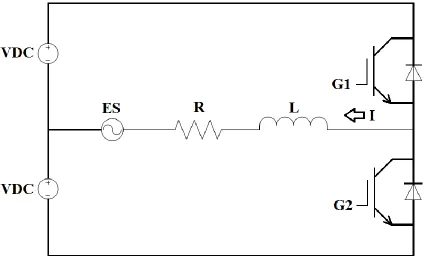
One of the most prevalent types of power electronic converter is the Voltage
Source Converter. This converter’s popularity arises from the fact that depending on the
controls used, it can perform several different applications. In its simplest form, the half
bridge VSC, the system is composed of two switching elements, a filter, a split bus, and a
load. (Figure 1.1) It is important to note that this load can represent several things
depending on the application. If this topology were to be used as a motor controller the
load would represent the current draw of the motor as well as the back electromotive
force. Here, a grid-tied converter is shown where the “load” is represented by a sinusoidal
voltage source.
Figure 1.1 Half Bridge Voltage Source Converter
When the current flowing through the branch is considered the output of the
ˆ
2 ,
1 , 1 1 [0, 0] x Ax Bu
y Cx Du
where
T
x I u VDC ES y I
R
A B C D
L L L
The transfer function between the converter voltage and current can then be found
through use of the Laplace transform. (1)
1 ( )
Giv s
R sL
(1)
As can be seen, the converter dynamics rely heavily on the parameter impedance
values. If these impedance values change during operation, the power converter can
suffer from performance degradation. In particular, the filter inductance is known to be a
component whose value can drift due to temperature, core material, and other operating
conditions. Previous work has shown that this changing inductance can have a
detrimental effect on the performance of such converts. [5] For this reason, it is desirable
to have a means of measuring such impedance values. Classical tools such as network
analyzers and dedicated inductance-capacitance-resistance meters perform an adequate
job but suffer from the fact that they are unable to make measurements while the
converters are in operation. This means that potential impedance values that change
during certain operating conditions could be overlooked. Ideally, one would measure the
impedance during operation to ensure that all of the characteristics are captured and
Previous research has already shown the feasibility of using a system’s switching
and sensing to affectively accomplish system identification. [6] [7] [8] These methods
rely on the ability of the converter to act as a network analyzer by injecting test sequences
into the system and measuring the response. This allows for the measurement of such
characteristics as voltage and current gain, as well as impedances of passive components.
While these techniques have proven to perform the job of system identification
admirably, they do require the injection of previously nonexistent perturbations into the
system, either through an intentional transient or some form of dithering. These
perturbations are minimized to ensure that control outputs are maintained within
acceptable limits while still exciting the system enough to make an accurate
measurement. For example, in a DC-DC converter the perturbations could increase the
output voltage ripple and inductor current ripple. Therefore, a tradeoff is made between
the amplitude of perturbation (related to the potential accuracy of identification) and
acceptable limits of output variation.
Beyond potentially increasing output ripple, these existing methods still have
some of the drawbacks of standard converters. One such drawback is the switching
harmonics present in most switching converters. [9] Switching harmonics are caused by
the fixed switching frequency and can lead to large currents at the switching frequency
and its harmonics. These harmonics are detrimental to the overall power quality and their
mitigation is of paramount importance. Traditional methods of filtering such as low pass
filters are affective, but for high power applications losses through these components and
component cost become significant. Alternatively, it has been shown that these
Essentially, by constantly varying the switching frequency, one can remove large
harmonic spikes and replace them with a wider band, flat noise spectrum. The objective
of this work is to use this flat frequency band injection as the test signal, while using
existing methods of identification to accurately measure system impedances for power
converters. This will achieve the goal of near-real-time impedance measurements, while
also having the advantage of minimized switching harmonics.
CHAPTER 2
P
ULSEW
IDTHM
ODULATIONVoltage source converters accomplish their control action through the use of
precisely timed switching signals. These switching states are determined by sampling
system outputs, and through means of a digital controller, calculating the necessary
switch mode. Methods of switching fall into two general categories, deterministic and
randomized. In the deterministic scheme, switching and sampling times are kept constant
based on a designed switching and sampling frequency. Randomized switching varies the
switching time , and possibly the sampling time, on a cycle-to-cycle basis. This chapter
will present three separate sub categories of modulation and examine how they affect the
operation of the system.
2.1 Deterministic Pulse Width Modulation
While there have been numerous forms of Deterministic Pulse Width Modulation
developed, each with its own advantages, they all share the common characteristic of a
set switching frequency. One of the simplest forms of DPWM is Carrier-Based Pulse
Width Modulation. With CBPWM, a triangular carrier wave is created and compared to
the controller’s generated reference signal. The switch states are then determined by
results of the comparison of the two waves. Here, a low frequency sinusoidal reference is
being compared to a much higher frequency carrier wave (Figure 2.1) which generates
Figure 2.1 Carrier Based Pulse Width Modulation comparison
Several factors go into the selection of a controller’s switching frequency. These
factors include, processor speed, system bandwidth, switch characteristics, and filter type.
It is desirable that the switching not add any disturbances to the system, so in practice
low pass filters are used to mitigate switching noise. The design engineer is tasked with
selecting a filter that will minimize noise while also considering factors such as filter
size, cost, complexity, and power loss. These compromises mean that the switching noise
can never be completely eliminated. Not only will noise be introduced at the switching
frequency, but also at harmonic orders of the switching frequency. In grid tied
applications this can decrease power quality, increase transformer heating, create acoustic
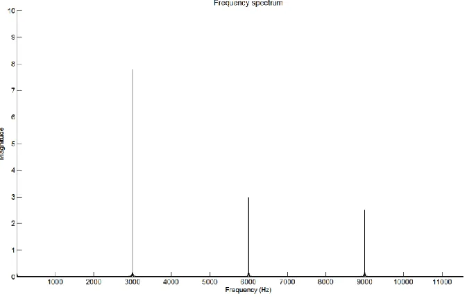
noise, and be potentially damaging to other equipment. [9] In the example of a Buck
converter using DPWM, these harmonics can easily be seen when viewing the frequency
spectrum of the system input current. (Figure 2.3)
It is not always feasible to reduce switching noise by increasing filter performance
as there may be design limits on the filter elements. For this reason, it is desirable to
minimize these harmonics through means other than simple passive filtering. One such
solution is the use of Randomized Pulse Width Modulation.
2.2 Randomized Pulse Width Modulation
In an attempt to mitigate injected switching noise without the use of extra
filtering, techniques for Randomized Pulse Width Modulation have been developed. At
the core of RPWM is the concept of a constantly varying switching frequency over a
predetermined frequency range. The goal of RPWM is to eliminate the characteristic
harmonic spikes cause by DPWM, and replace them with a wide band of noise. While
there is still noise being injected, spreading it across a frequency band is advantageous to
the elimination of acoustic noise, possible grid damage, and power quality issues. [9]
2.2.1 Randomized Carrier Frequency PWM
One method of RPWM is the use of a randomly varying switching frequency.
With deterministic CBPWM, the frequency of the carrier wave is held constant, leading
to the aforementioned harmonic current spikes. In contrast, randomized carrier based
PWM is achieved by changing the slope of the carrier wave on a cycle by cycle basis. As
CBPWM switching frequency is based upon the intersection of the carrier wave and the
reference wave, increasing the carrier wave slope increases the switching frequency while
Figure 2.4 Randomized switching frequency carrier based PWM
While this method of RPWM achieves the desired goal of modulating the
switching frequency, it does have drawbacks when implemented in an actual system. One
of the main concerns with this type of implementation is the connection between
switching frequency and sampling frequency. (Figure 2.5)
As can be seen, the sampling time is no longer constant; rather, it is constantly
changing in synchronization with the randomized switching frequency. This makes the
implementation of a digital controller very difficult as the sampling time step is used in
the calculation of future outputs. This also limits the minimum switching time (maximum
switching frequency) to the time necessary for a control iteration. Ultimately, this means
the maximum switching frequency is limited by factors such as ADC sampling times,
control algorithm execution times, and any other controller overhead. For these reasons,
it is beneficial to use a system of RPWM that decouples the switching frequency from the
system sampling time.
2.2.2 RPWM II
A system of randomized pulse width modulation has been developed that
provides the advantages of RPWM (minimized harmonic injections), while having the
added benefit of a fixed sample time. [9] This method, here called RPWMII, uses a fixed
sampling frequency and a randomly generated time delay between the start of subsequent
switching cycles. This time delay, denoted Δt, is calculated by (2) where is a random
number varying over the range 0 to 1, and τ is the sampling period.
t r
(2)
Care must be taken when calculating values of Δt as they could inadvertently
exceed the limitations of the system. To avoid possible collisions, the switching period is
limited to values between and 2τ. The limit ensures that any operations of the controller (sampling, communications, calculations, etc.) can be completed before the
Figure 2.6 RPWMII timing scheme
The RPWMII algorithm [10] is simulated in MATLAB and Simulink to
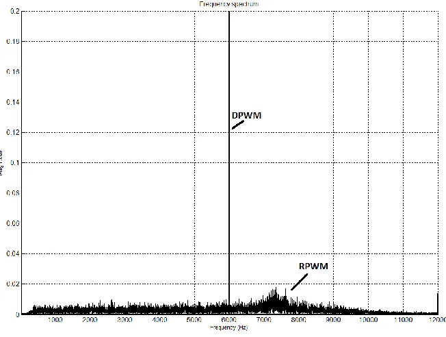
determine the effectiveness of harmonic mitigation. (Figure 2.7) When compared to the
same circuit using DPWM switching at 6kHz, it can easily be seen that the characteristic
harmonic spikes have been eliminated and replaced with a wide distribution in the
frequency spectrum.
Not only does RPWMII serve to minimize the harmonic current spikes, but it has
the added benefit of injecting a wide-bandwidth sequence into the system. The next
chapter will discuss how this sequence can be used to perform system identification
CHAPTER 3
S
YSTEMI
DENTIFICATIONThere are several existing methods of identification designed for a multitude of
different systems. These approaches are used to model several types of systems ranging
from the dynamics of an industrial process to the steering controls of large ships and
more importantly the open-loop characteristics of switching converters. [11] The general
concept of each type of system identification is to measure inputs and outputs, then
through some method, develop a mathematical model of the system in question. With a
model in hand, a control scheme can be created, or in the case of on-line identification, an
existing controller can be honed to improve performance.
3.1 Previous Methods of Identification
With so many possible methods of identification available, it is necessary to
determine the proper technique for the given situation. Considerations must be made
regarding desired accuracy, measurements available, type of system under test, and
physical limitations of the measurement equipment. All of these methods take advantage
of the fact that switching converters already have sensors in place to measure necessary
voltages and currents. This essentially allows the switching converter to measure its own
3.1.1 Step Response
One of the simplest methods for identification of an unknown system is the step
response technique. This type of identification is commonly used for the modeling of
industrial processes such as material level controls, heating and cooling, and speed
controllers. [12] [13] For a first-order, linear system ,the process attempts to approximate
the necessary gain, K, and time constant, T, to match with a first-order model (3).
) ( 1 )
( U s
Ts K s
Y
(3)
As can be seen in the above equation, the system input, U(s), and output, Y(s),
can be used to calculate the desired model parameters. During the identification, the input
is carefully given a step change while the output is closely monitored. These are the
values then used to construct the simple system model. While this is an effective and
often used method for system identification, it does have disadvantages. The need for a
step change requires that the output be altered by some non-negligible amount. This may
be acceptable if the system is offline or if the step size can be minimized, but often the
step needs to be relatively large to rise above the noise present in the system. If this were
to be used for a grid tied converter, it would be necessary to ensure that the grid could
handle the transients introduced. Also, the difficulty in model matching increases with the
order of the system to the point where complex non-linear systems may not be able to be
identified.
3.1.2 Cross-Correlation Methods
correlation system does not require any large transients to excite the device under test.
Instead, a wide-bandwidth test sequence is injected into the switching converter control
signal and the voltages and currents are measured to determine the desired system
parameters. [6] [7] [8] This method has been shown to be very effective in determining
things such as the control-to-output transfer function as well as system impedances.
At the core of this technique is the ability to inject a suitable test sequence into the
control of the converter under test. A sampled switching converter operating in steady
state can be described by (4)
[ ] [ ] [ ] [ ] 1
y n h k u n k v n k
(4)Here, is the sampled output, is the discrete-time system impulse
response. is the sampled input, and is any noise in the system. In a switching
converter, the input represents the PWM control signal and the output can be measured
voltages or currents. When the cross correlation of the input and output is taken, (4)
becomes (5).
R [ ] [n]R [m n] [m] 1
n h R
uy uu uv
n
(5)If we assume the input signal to be white noise to meet the aforementioned
requirement of a wide-bandwidth injection, assumptions can be made regarding the
parameters in (5). For true white noise, an equal frequency spectrum over an infinite band
of frequencies, the following holds true for the autocorrelation of the input (6) and the
[ ] [ ]
Ruu m m (6)
[ ] 0
Ruv m (7)
Here, represents the system discrete impulse signal and when put into (5)
leads to the simplified equation for input-to-output cross-correlation. (8) If the discrete
Fourier transform (DFT) is then taken, the result is the input-to-output transfer function.
(9)
[ ] [ ]
Ruy m h m (8)
[ejw] DFT{h[m]}
Guy (9)
As the sensed outputs of most power converters are voltage and current, two
distinct transfer functions can be found: control-to-voltage and control-to-current . If impedance measurement is the goal, Ohm’s law can be used as such.
(10)
ˆ[e ]
ˆ ˆ
[e ] [e ] [e ]
[e ]
ˆ ˆ
[e ] i[e ] i[e ] ˆ[e ]
j v
j j j
Gvd d v Z j
j j j
Gid j d
(10)
This can be further simplified to show that for impedance measurements, it is only
necessary to take the ratio of the DFT of the measured voltage and current. (11)
{ [ ]}
[e ] { [ ]}
DFT v n j
Z DFT i n
Previously, an assumption was made that the input test sequence could be
approximated as pure white noise. While examination of this assumption is outside the
scope of this paper, some general observations can be made. Firstly, in previous work the
test sequence utilized the superposition of a pseudo-random binary sequence (PRBS)
upon the system control signal. This effectively dithers the PWM over a set range of
frequencies. The upper limit of this injected frequency is limited to ⁄ by the Nyquist criterion, where is the system sampling frequency. The lower frequency limit and frequency resolution is determined by the PRBS length. In general, a tradeoff of
a higher frequency band can be achieved at the cost of increased computational
requirements such as time and memory. The literature has shown that this is an effective
means of system identification, particularly with the measurement of impedances, though
it does still have its limitations.
The PRBS injection works by either adding or subtracting some small amount of
time to the switching cycles, on a cycle by cycle basis. This means that the switching
Figure 3.1 Switching states of PRBS versus DPWM
Because there are only two possible switching frequencies during an injection,
large harmonic spikes are still present as in standard DPWM switching. When the
frequency spectrum of a converter using DPWM (Figure 3.2) and one undergoing a
PRBS injection (Figure 3.3) are compared, they look very similar. Both have the
characteristic spikes at the switching frequency and its harmonics, while the PRBS
Figure 3.2 DPWM current frequency spectrum
Figure 3.3 PRBS current frequency spectrum
For this reason, this identification method will be modified to use RPWMII as the
extra equipment (sensors) while simultaneously providing the advantages of reduced
harmonic injections.
3.2 RPWM for System Identification
System identification using RPWM has two distinct advantages. First, as will be
shown, it does an adequate job of identifying system impedances within the range of
injected frequencies. Secondly, as was shown in Figure 2.7, harmonic current spikes of
switching converters can be greatly reduced without the need for extra filtering
components. As opposed to the other methods described at the beginning of Chapter 3
that require the deliberate injection of some type of test sequence, RPWMII is constantly
injecting frequency information into the system. This also means that there will be no
difference in outputs, be it voltage or current, between the identification state and normal
operation.
As discussed in section 2.2.2, there are natural limits to the range of injected
switching frequencies. The aforementioned and 2τ correspond to the maximum injected frequency and minimum injected frequency respectively. Because the limits on
possible switching frequencies are determined by the RPWMII algorithm, they will be
held constant throughout experimentation. As long as the method of randomization
within the RPWMII algorithm is truly random, the injected frequencies are evenly
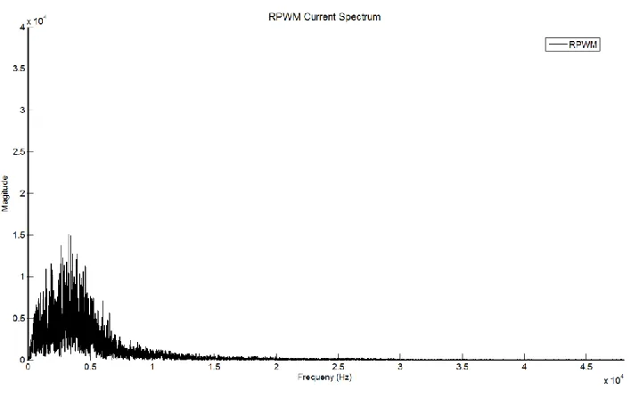
distributed over the defined range of frequencies. The frequency spectrum of a switching
converter utilizing RPWMII clearly shows a “bleeding” of the spectral information down
into the sub switching frequencies. (Figure 3.4) These frequencies correspond to the
Figure 3.4 RPWMII current frequency spectrum
These injected frequencies serve as an analog to the PRBS injection in the
cross-correlation technique. Like the cross-cross-correlation technique, the first step of identification
is the injection of a suitable test sequence. The second step is the conversion of the
measured time domain data into the frequency domain. As this will be a sampled digital
system, the digital Fourier transform will be used. (12)
2
1 ( ) kn
1
[ ] [ ]
0
N j
N
x n X k e
N k
n0,1, 2,..., N 1 (12)By applying the DFT to the sampled voltages and currents, the system response at
distinct frequencies can be identified. Knowing the system voltages and currents over the
injected frequency range means that the system impedances can easily be calculated by
do a final conversion to find the magnitude (13)
2 2
(RealPart) (ImaginaryPart)
Magnitude (13)
With these values, a classical Bode plot can be formed by plotting the magnitude
versus frequency on a semilog axis. From here, the desired impedance, such as
inductance, can be calculated through means that will be discussed in Chapter 4. Of
particular importance are filtering and averaging techniques required to get reliable
CHAPTER
4
I
MPLEMENTATIONThis chapter focuses on the implementation of the previously discussed
techniques of identification. First, a generalized identification routine is developed. This
routine is meant to serve as a template for identification of any type of system impedance.
Next, data fitting algorithms are discussed in detail. Finally these routines are simulated
for two separate converter topologies using MATLAB and Simulink. A level-two
MATLAB s-function has been created to achieve the RPWMII algorithm and can be
found in Appendix A. This s-function allows for variations in the switching frequency
and the random frequency range to be tested. All simulations are carried out in the fixed
time step mode to provide evenly spaced sampled data. Simulation times are set to at
least 50 times faster than the desired switching frequency to provide the best results. As
the RPWMII s-function is counter based, these very low simulation steps provide more
accurate switching at the cost of increased simulation times. The data output from the
fixed step mode will be equivalently sampled at a sampling frequency equal to the
inverse of the simulation time. This sampling frequency will be on the order of several
megahertz, much higher than in a realistic implementation, so down sampling of the data
will be done after the simulations are complete. Setting the simulation time to even
multiples of the desired sampling frequency also makes the future down sampling
simpler. Processing the sampled data after simulations instead of during the runs allows
sample times. As the simulations tend to be long, roughly 500 times slower than
real-time, this method has the added benefit of gathering data once and executing the
relatively fast post processing with varying parameters.
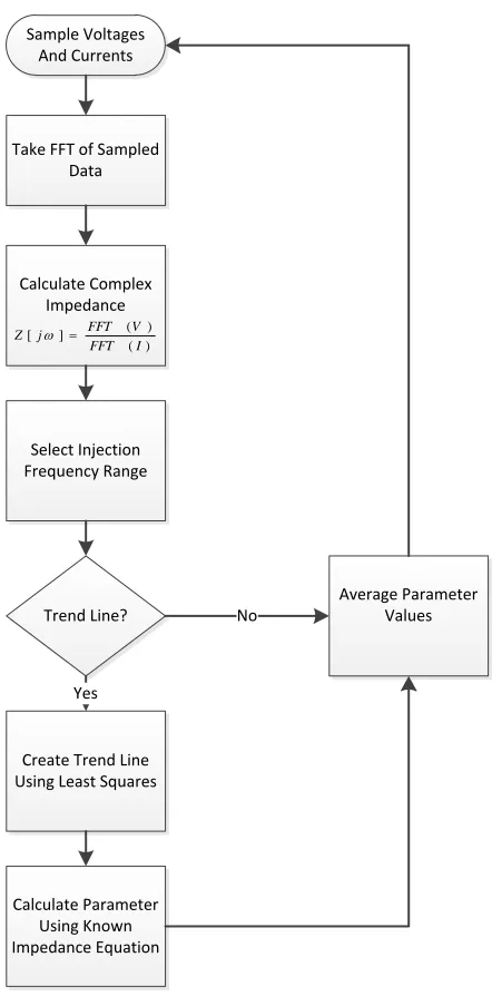
4.1 Identification Routine
Until this point, the methods of identification have been discussed in general
terms without a defined identification routine. This section is meant to develop a standard
procedure that can be used to identify any type of impedance in the system. The first step
is to measurement the necessary voltages and currents. The selection of the sampling
frequency is important as it will limit the maximum identifiable frequency to Fsample 2
by the Nyquist criterion. Care must be taken to set this sampling frequency well enough
above the injection frequency range to ensure accurate impedance estimation. In the case
of the following simulations, a sampling frequency slightly higher than twice the
maximum injected frequency ensures the widest sampled band of data possible. Next, the
FFT of the sampled voltages and currents must be taken to transform the sampled time
domain data into the frequency domain. With this frequency domain data, the complex
impedance can be calculated using Ohm’s Law by simply taking the ratio of the FFT
voltage and FFT current. Taking the magnitude of this resultant complex impedance
yields the magnitude of the measured impedance. As the RPWMII injects frequencies
over a known range, this is the series of frequencies over which a numeric impedance
estimation will be made. At this point, there are two possible methods (discussed in detail
below) for calculating a numeric value for the circuit parameter in question. Both
a known resistor value, capacitance can be calculated using the measured impedance
data, the frequency at that impedance value, the known resistor value, and the equation
for the magnitude of the impedance. This general methodology is shown here. (Figure
4.1)
Sample Voltages And Currents
Take FFT of Sampled Data Calculate Complex Impedance ) ( ) ( ] [ I FFT V FFT j
Z
Select Injection Frequency Range
Trend Line?
Create Trend Line Using Least Squares
Yes Calculate Parameter Using Known Impedance Equation Average Parameter Values No
4.2 Measured Impedance Averaging
The first method of numeric impedance calculation is to average a large number
of calculated values over the injected frequency spectrum. With this method, the
parameter in question, for example capacitance, is calculated for each frequency within
the injected range. This vector of values can then be averaged to yield an approximate
value for the measured capacitance. This method relies on the RPWMII injection to
provide ample data within the frequency range. The averaging routine could be optimized
for a real controller by implementing concepts such as a moving average. This technique
does require several calculations, defined by the number of points selected within the
injected frequency range. An example of this technique can be found in Section 4.4
where the inductance value of a Buck converter is calculated.
4.3 Least Squares Fitting
While the previous method does show promise for numeric impedance
approximation, the results rely on the average of a large number of values for best results.
If large outliers are present in the reconstructed impedance plot, the results can be
skewed, leading to a higher percentage of error. For this reason, the improved method of
identification will utilize a trend line step before the parameter calculation routine. This
trend line calculation will help eliminate the large outliers. One such trending algorithm
is Linear Least Squares fitting. [14] The least squares method attempts to minimize error
in a signal and is common for data fitting. This procedure uses the measured data over the
injection range to calculate a Y-intercept, and a slope, that will form the trend line.
2
2 ( )2
Y X X XY
b
n X X
(14)2 ( )2
n XY X Y
m
n X X
(15)ymx b (16)
For the purpose of impedance reconstruction, X represents frequency while Y
represents the measured magnitude. Once the impedance magnitude has been calculated,
the values for the trend line are determined. The values on this trend line are then the
values used to calculate the desired parameter in question. While this method is
essentially adding another step to the calculation process, it has shown to improve the
results and minimize the percent error. The MATLAB function used for this trending
portion can be found in Appendix C.
4.4 Buck Converter
The buck converter is one of the most common types of converters used for
stepping down one DC voltage to a lower DC level. [15] While there are several
possibilities as far as switching elements (MOSFETs, diodes, or IGBTs) here ideal
Figure 4.2 Buck converter with ideal switches
Buck converters accomplish their voltage regulation through control of the
switched current seen by the inductor. By varying the amount of time the upper switch is
on in relation to the lower switch, the output voltage level can be controlled. At the
switching node, the voltage produced is a square wave with a frequency equal to the
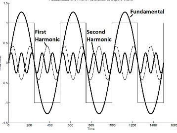
switching frequency. When viewed as a sum of sinusoids, it is clear to see that this square
wave will inject noise at the fundamental switching frequency as well as its numeric
harmonics. Here, an arbitrary square wave is shown along with its first three sinusoidal
Figure 4.3 Square wave with harmonics
To achieve the desired DC output voltage, a low pass filter is formed by the
inductor and capacitor. Careful selection of these filter elements can reduce the hard
switching square wave to a DC value with minimal voltage ripple. This type of converter
often senses the switched current as well as the output voltage making it possible,
through the aforementioned methods, to identify the inductor’s value.
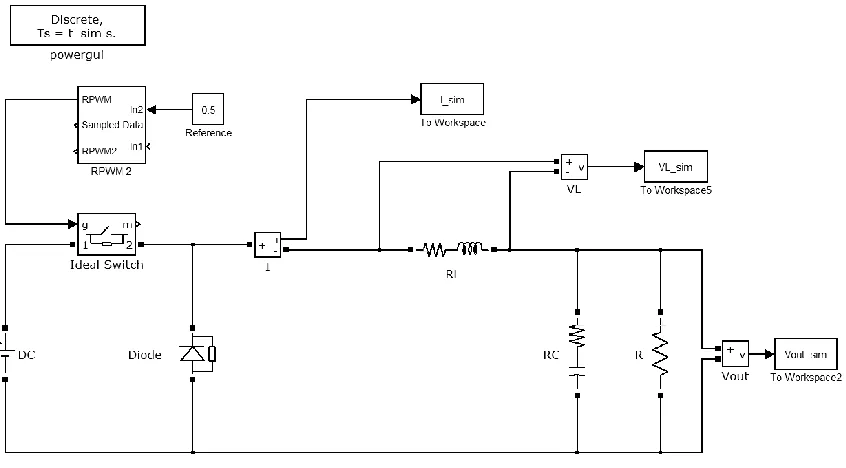
The buck converter simulation is carried out using MATLAB and Simulink. As
can be seen, the high side switch is realized through an ideal switch while the low side
consists of a diode. (Figure 4.4) Common component parasitics such inductor and
capacitor series resistances have been included to more closely match a realistic
Figure 4.4 Buck converter used for simulation
As can be seen in the schematic, measurements are made and saved to the
MATLAB workspace for inductor current, inductor voltage, and output voltage. It should
be noted that in a physical implementation, the differential inductor voltage is not
measured directly, but could be reconstructed by taking the difference of the output
voltage and the known switching state. This allows for the possibility of measuring
several different system impedances as validation of the concepts of impedance
identification. Before implementing RPWMII, a control simulation is run using standard
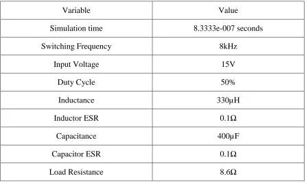
DPWM. All important simulation values can be found in Table 4.1. Outputs are down
sampled to a 24 kHz sampling rate to reflect a more realistic sampling frequency. For this
Table 4.1 Simulation Values for DPWM Buck Converter
Variable Value
Simulation time 8.3333e-007 seconds
Switching Frequency 8kHz
Input Voltage 15V
Duty Cycle 50%
Inductance 330µH
Inductor ESR 0.1Ω
Capacitance 400µF
Capacitor ESR 0.1Ω
Figure 4.5 Current frequency spectrum of DPRM buck converter simulation
Due to the set switching frequency, the measured current spectrum has a
characteristic spike at 8 kHz. (Figure 4.5) Next, a simulation is run using the custom
RPWMII s-function block. Here, all component values have been kept the same, the only
difference is the switching frequency will not vary over the range of 4000 to 9000 Hz.
The current frequency spectrum shows the dramatic reduction in large harmonic spikes.
(Figure 4.6) Note that when comparing Figure 4.5 and 4.6, different scales are used for
the Y-axis. This was done to help show the general shape of the injected frequency
Figure 4.6 RPWMII current frequency spectrum
If we try to construct an impedance plot using the output voltage and measured
current we would expect to see the parallel combination of the filter capacitor and it’s
ESR with the output resistance. In terms of ω this impedance would be
The Bode plot of this function shows the characteristic downward slope attributed
Figure 4.7 Expected Bode plot for
Using the measured output voltage and inductor current from the RPWMII
simulation, a fairly accurate impedance reconstruction can be made. (Figure 4.8) As can
be seen in the plots, most of the salient features of the transfer function can be observed
including the load resistance, ESR, and the capacitor induced slope. It is important to
note that the tightest reconstruction occurs around the injection frequency range and tends
away as the frequency approaches zero. It can also be seen that there is a fair amount of
Figure 4.8 Constructed impedance using RPWMII
To minimize these erroneous data points and provide a tighter reconstruction, the
averaging step is used. The averaging routine improves with the number of sampling
periods used at the cost of increased calculation time. The results of the averaging
function, found in Appendix B, show a much tighter reconstruction about the actual
impedance. Here, the same impedance is recreated while sampling the FFT over two
sample lengths. (Figure 4.9) As can be seen, most of the outliers have been eliminated,
Figure 4.9 Constructed impedance using RPWMII and averaging
While this impedance reconstruction is interesting, for the sake of controls we
would prefer to identify the inductor element. The same simulation data is used, but this
time we will take the FFT of the inductor voltage. When the same process of averaging is
used the following Bode plot is generated, showing the measured and actual value for an
Figure 4.10 Constructed RL impedance using RPWMII and averaging
As can be seen, outside of the range of frequencies injected by the RPWMII
signal, the measured impedance quickly trends away from the actual value. If we look at
just the range of injected frequencies, here 4 kHz to 9 kHz, the matching is much clearer.
Figure 4.11 Constructed RL impedance using RPWMII and averaging ZOOM
Since it is desired to have a numeric value for the measured inductance, it is
necessary to perform a fitting algorithm to the measured impedance plot. For this
parametric fitting there are essentially two variables, the inductance and the built in
resistance of the inductor. If the rated inductor resistance is considered a constant, a fairly
accurate approximation of the inductance can be made by using the equation for the
magnitude of the RL impedance. (17)
2 2
| Z(j 2 f) | RL (j 2 f L) (17)
Solving (17) for L leads to the following equation (18) which contains one
2 2 (| Z(j 2 *f) |)
2 2 4 RL L f
(18)
With (18) it is possible to calculate the unknown inductance by using the
impedance magnitude from the reconstruction step and the known inductor resistance.
The inductance calculation begins by slicing just the frequencies of interest. This is a
simple step as the results of the FFT are stored as an array of magnitudes versus
frequency, and the injected frequency range is selected during the design phase of the
controller. Next, the inductance is calculated at each frequency within the range. It should
be noted that it is not necessary to iterate through each frequency over the range, but a
higher number of points used will result in a better average. Careful design of the final
code would also allow for a somewhat parallel solving structure where the inductance
value is being calculated while the next set of voltages and currents are being sampled.
Multiple simulations confirm the viability of this averaging technique for
identifying the system inductance assuming a constant inductor resistance value. Three
separate simulations show that the inductance value can be found with less than 10%
error. (Table 4.2) For each simulation the frequency range for inductor averaging has
been selected to be 5 kHz to 6 kHz as it falls within the heart of the injected frequencies.
Table 4.2 Simulation Results for Inductance Calculation
Actual Value Calculated Value Percent Error
165µH 176µH 7.1%
330µH 345µH 4.5%
Though it is outside the scope of this research, these calculated inductance values
could then be used to update the inductance value used within the closed loop controller.
The literature has shown the improvements possible when the inductance can be updated
in real time. [16]
4.5 Single Phase Grid-Tied Converter
The next converter of interest is the single phase grid-tied converter. The grid-tied
converter can easily be implemented as an active rectifier, an inverter, or for use with
energy flow management. The single phase case is used as it reduces the number of
measurements necessary and serves as a good approximation for the balanced three phase
converter. (Figure 4.12) For an actual implementation, special care will be needed to
ensure the proper voltages are measured. [17]
The process of identification is similar to that used for the DC-DC buck converter,
the difference being there will now be additional low frequency harmonics present in the
system. These harmonics arise due to the fact that there is now a sinusoidal voltage and
current being produced. This fundamental frequency is often much lower than the
switching frequency, and in this simulation it will be set at 60Hz to match the US power
grid. (Figure 4.13)
Figure 4.13 Grid-tied converter simulation
As with the Buck converter, the first simulation uses a standard DPWM to serve
as a baseline. A one-arm universal bridge is used with the gate signals generated by a
CBPWM. The grid is simulated by an AC voltage source with a resistive-inductive grid
impedance. All relevant simulation values are listed in Table 4.3. The current spectrum
contains the typical spike at the switching frequency, but now there are also frequency
Table 4.3 Simulation Values for DPWM Grid-Tied Inverter
Variable Value
AC source maximum amplitude 300 V
AC source frequency 60 Hz
Grid Inductance 1 mH
Grid Resistance 10 mΩ
Filter Inductance 10 mH
Filter Resistance 28 mΩ
Switching Frequency 8 kHz
The DPWM is then replaced with the custom RPWMII block with an injection
range of 5 kHz to 9 kHz. As expected, the large spike at the switching frequency has been
replaced by a wide spectrum frequency injection. (Figure 4.15) The frequency
reconstruction also shows a much closer fitting to the actual impedance value within the
injected frequency range. (Figure 4.16) Using the same method as that used for the buck
converter, a numeric value is found for the filter inductance.
Figure 4.16 RPWMII Inverter impedance reconstruction ZOOM
Several simulations confirm the viability of these methods for inductance
estimation using RPWMII. Table 4.4 shows the calculated versus real values and
compares the averaging method with the least squares fitting method.
Table 4.4 Improvements Using Least Squares Fitting
Simulation Calculated Without Fitting (percent error)
Calculated With Fitting (percent error)
R=28mΩ L=10mH 10.7 mH (6.9) 10.4 mH (4.8)
R=28mΩ L=5mH 6.0 mH (21.2) 5.6 mH (11.4)
R=28mΩ L=2mH 2.5 mH (23.0) 2.3 mH (12.8)
As can be seen, the methods developed for the Buck converter also work very
well for the grid-tied converter. The frequency components created by the grid
fundamental do little to corrupt the estimated impedance value as they exist much lower
CHAPTER
5
H
ARDWARE VALIDATIONTo confirm the findings of the simulation, a low power Buck converter has been
built to closely match the one in simulation. Special consideration has been made when
selecting components to account for parasitics. Each passive component is measured with
an Agilent U1733C LCR meter over a range of frequencies with the average results found
in Table 5.1.
Table 5.1 Actual Component Values for Buck Converter
Component Rated Value Measured Value
Inductor 330µH 333µH
Inductor DC Resistance N/A 0.54Ω
Capacitor 470µF 420µF
Capacitor ESR N/A 0.23Ω
Load Resistor 10Ω 10.1Ω
The controller used is the PIC32MX460F512L-80I/PT from Microchip built on a
custom carrier board. This particular controller can operate up to 80 MHz which will
allow for finer resolution of the generated RPWM. The onboard ADCs will not be used
as the excess overhead necessary would quickly outpace the abilities of the controller.
rate of 24 kHz which is in line with the simulations. The use of the data acquisition unit
has the added benefit of being able to easily export the measured data in a format that can
be read by MATLAB. This means that the same fitting code used for the simulations can
be used on the measured data. Voltage is measured directly while the current is measured
using the ACS712ELCTR-30A current sensor on a custom made sensor board. (Figure
5.1)
Figure 5.1 Current sensor schematic
To match the simulations, the first impedance measured is the parallel
combination of the output capacitor and load resistor. The following plots show the
measured reconstruction of the selected impedance versus the actual impedance for two
Figure 5.2 Hardware validation C = 470µF
Figure 5.3 Hardware Validation C = 800µF
Much like the simulations, both reconstructions follow the actual impedance very
closely. The change in corner frequency as well as the difference in ESR is clearly
be noted that while there is a spike on the frequency spectrum, its magnitude is relatively
small and is most likely caused by the limited resolution of the controller’s RPWM
sequence. In terms of impedance measurement, its presence goes unnoticed.
Figure 5.4 Measured current frequency spectrum
Next, the previous methods for inductor estimation are used to calculate the value
of the real components. It is important to note that while the inductor voltage could be
determined by the known converter switch states and output voltage, here a differential
voltage measurement is made across the inductor. For the particular data acquisition unit
used, the sampling frequency for three channels (current, output voltage, and switched
voltage) reduces the maximum sampling frequency to 16kHz. This in turn limits the
maximum identifiable frequency to 8kHz. Below are the impedance reconstructions using
two separate inductor values, showing just the range of injected frequencies. (Figure 5.5
Figure 5.5 Impedance reconstruction with L=330µH
These impedance reconstructions show a close matching to the expected actual
values. When numeric values for inductance are calculated, the results are very
promising. (Table 5.2) Factors such as measurement error have been eliminated as much
as possible by calibrating the sensors against known voltage and current sources.
Table 5.2 Calculated Inductance Values
Rated Inductance Calculated Without Fitting (percent error)
Calculated With Fitting (percent error)
330µH 372µH (12.6) 367µH (11.3)
CHAPTER
6
P
RACTICALC
ONSIDERATIONS FOR IDENTIFICATIONThe goal of this thesis is to develop a method for impedance identification for real
systems. That makes it necessary to consider practical limitations of the system when
developing these procedures.
6.1 Sampling Time and Frequency
As the DFT is a summation of multiplications, it can quickly become
computationally taxing. For this reason, fast Fourier transforms will be used. The FFT is
able to reduce the number of operations to as opposed to for the more
general Fourier transform. [18] Most modern digital signal processors contain highly
efficient FFT functions that simplify the implementation of these techniques. The total
execution time of the FFT algorithm is determined by the processor execution time, and
the length of the sampled data. Table 6.1 demonstrates the time savings possible by using
the FFT over the standard Fourier transform.
Table 6.1 Execution Comparison Between Fourier Transform and FFT
Number of Samples Fourier Transform
Number of cycles
FFT
Number of cycles
128 16384 621
256 65536 1420
512 262144 3194
The FFT length is determined by both the system sampling frequency, and the
length of the sampling period. The sampling frequency and the sampling period both play
a role in the final resolution in the frequency domain. This resolution is the maximum
number of Hz between any two given samples after preforming the FFT and is calculated
by (19)
number of samples frequency resolution
sample frequency
(19)
This frequency resolution is important as it is one of the determining factors in the
final quality of the system identification. If we consider a simple RL circuit, the
frequency resolution determines the change in inductor value it would be possible to
identify under ideal conditions. (Figure 6.1) In this example, a fixed resistance of 10Ω is
used while the inductor value is changed from 1mH to 1.5mH. At the 3dB point of each
graph, there is a difference of approximately 50Hz between the two plots. Therefore, if
the goal was to distinguish between inductances of 1mH and 1.5mH at their
corresponding corner frequencies, the frequency resolution would need to be at least
Figure 6.1 Importance of frequency resolution
Ideally, one would use the longest sample period possible to provide for the
highest possible frequency resolution. Practically speaking, this sampling period is
limited by two factors; how frequently identification is needed, and memory restrictions
of the controller. Consequently, physical parameters of the controller as well as desired
identification resolution determine the sample period length and in turn, the maximum
frequency resolution.
6.2 Sampling Resolution
Another factor in determining the accuracy of identification is the precision of the
measuring devices. Possible measurement error falls under two main categories:
or ADC. Much like the aforementioned frequency resolution, the ability to discern
between two possible impedance values is limited by the measurement resolution. The
Bode plot of two simple RL circuits is shown below. (Figure 6.2) For both plots, the
inductance is held constant at 1mH while the resistance is changed from 5Ω to 7Ω. It is
clear to see that for frequencies in the region of 250Hz, the two magnitudes differ by only
3dB. This requires that the ADC be able to discern at least this 3dB difference to be able
to identify a change in resistance of 2Ω.
Figure 6.2 Importance of ADC resolution to identification
Not only is the relative accuracy of the measurement important, but so too is the
linearity of the sensor and ADC. For simple control systems, it is often assumed that the
feedback system is purely a frequency independent gain block. In reality, feedback
amplifiers, filters, and any system parasitics. Because the final goal of identification is to
gather frequency dependent information, it is crucial that any frequency distortion
introduced by the feedback network be well above the range of frequencies of interest. If
the feedback loop attenuates frequencies within the identification band, the values may
become too small to discern from the existing noise. For example, the ADS7863 from
Texas Instruments is a dual, 12-bit ADC capable of sampling rates up to 2MSPS. From
the datasheet it can be seen that with an increase in frequency there is also a decrease in
the signal to noise ratio and an increase in total harmonic distortion. (Figure 6.3)
Figure 6.3 Typical ADC frequency characteristics (TI ADS7863)
When selecting components for such systems, it is important to ensure that
nothing in the sensing loop will add unknown frequency distortion. As the region of
interest is below the switching frequency, the feedback loop should already meet these
requirements, but it is still good practice to ensure there will not be any unnecessary error
CHAPTER
7
C
ONCLUSION AND FUTURE WORKThe objective of this work is to show the viability of using Randomized Pulse
Width Modulation as a means of impedance identification in switching power converters
while also minimizing the amount of harmonic noise. By monitoring the impedance of
elements within the control loop, digital controllers can adapt and perform a better job of
regulating the outputs. This in turn can lead to more efficient controllers, as well as the
use of cheaper components that have a higher variation from their normal value as well as
a greater degree of non-linearity.
The use of RPWMII as a source of accurate impedance estimation while also
reducing injected harmonics has been demonstrated. Using the power converter’s existing
voltage and current sensors, the necessary values are sampled at a fixed frequency. Fast
Fourier transforms are then used to convert this time domain data into the frequency
domain. A complex impedance value can then be calculated using these voltage and
currents and Ohm’s law. Next, a trend line is created using the least squares fitting
algorithm to help eliminate any spurious noise present in the measurements. The
parameter value in question can then be solved for using the known impedance equation
and the measured complex impedance over the range of injected frequencies. These
methods have proven to be accurate in the estimation of impedances with DC as well as
AC systems. Simulations have shown a percent error of less than 10 percent when
simulation findings have also been validated through hardware testing on a low powered
Buck converter. The concept of harmonic reduction through the use of RPWMII has also
been confirmed. By spreading injected noise over a wider frequency spectrum, the large
spikes common with standard switching techniques can be greatly reduced. This achieves
the desired goal of converter element impedance estimation while simultaneously
reducing harmful harmonic injections.
Future Work
As the main focus of this research is on the development of the use of RPWMII
for impedance estimation, a smaller amount of time has been spent on implementing the
results of such measurements. Future work could use these measured impedances to
update closed loop control systems in real time. To implement these techniques into a
final physical device would require careful attention to the abilities of the controller as
well as the structure of the overall program. As great quantities of sampled data are being
stored locally, large amounts of robust, fast memory would be necessary. The feasibility
of such systems should only improve with time as the cost of more capable devices and
memory are trending downwards. Also, ongoing developments in the field of Digital
Signal Processing have shown the possibility of even more efficient FFT algorithms. [19]
Such “sparse” FFT implementations could lessen the requirements of the identification
system.
One interesting possibility is the use of machine learning to improve the
impedance estimations. The methods used here are admittedly simplistic in their attempts
constantly evolving systems. Such a system could possibly recognize and act on patterns
R
EFERENCES[1] Ming-Tsung, "Analysis and Design of Three-Phase AC-to-DC Converters With High Power Factor and Near-Optimim Feedforward," IEEE Transactions on Industrial Electronics, vol. 46, no. 3, pp. 535-543, 1999.
[2] M. P. Kazmierkowski, "Review of Current Regulation Techniques For Three-Phase PWM Inverters," in IEEE ISIE, 1993.
[3] A. L. Trigo, "A Linear Time Model of The Voltage Source Converter for STATCOM Applications," in PSCC, Liege, 2005.
[4] P. Lehn, "Exact Modeling of the Voltage Source Converter," IEEE Transactions on Power Delivery, vol. 17, no. 1, pp. 217-222, 2002.
[5] D. Martin, "Auto Tuning of Digital Deadbeat Current Controller for Grid Tied Inverters Using Wide Bandwidth Impedance Identification," IEEE, pp. 277-284, 2012.
[6] B. Miao, "System Identification of Power Converters With Digital Contol Through Cross-Correlation Methods," IEEE, pp. 1093-1099, 2005.
[7] D. Martin, "Wide Bandwidth System Identification of AC System Impednace by Applying Perturbations to an Existing Converter," IEEE, pp. 2549-2556, 2011.
[8] A. Barkley, "Improved Online Identification of Switching Converters Using Digital Network Analyzer Techniques," in Power Electronics Speacialists Conference,
PESC 2008. IEEE, 2008.
[9] K. Borisov, "Experimental Investigation of Submarine Drive Model With PWM-Based Attenuation of Acoustic and Electromagnetic Noise," University of Nevada, Reno, 2003.
2007.
[11] L. Ljung, System Identification: Theory for the User, Englewood Cliffs: Prentice-Hall, 1987.
[12] Q. Bi, "Robust Identification of First-order Plus Dead-time Model from Step Response," Control Engineering Practice , vol. 7, pp. 71-77, 1999.
[13] S. Ahmed, "Novel Identification Method from Step Response," Control Engineering Practice, vol. 15, pp. 545-556, 2007.
[14] D. S. Moore, The Basic Practice of Statistics 3rd Edition, New York: W. H. Freeman and Company, 2004.
[15] R. W. Erickson, Fundamentals of Power Electronics Second Edition, Norwell: Kluwer Academic Publishers, 2001.
[16] A. Barkley, "Adaptive Control of Power Converters Using Digital Network Analyzer Techniques," University of South Carolina, Columbia .
[17] D. Martin, "Wide Bandwidth Three-Phase Impedance Identification using Existing Power Electronics Inverter," IEEE, pp. 334-341, 2013.
[18] J. H. McClellan, DSP First, Upper Saddle River: Prentice-Hall, 1999.
[19] H. Hassaneih, "Simple and Practical Algorithm for Sparse Fourier Transform," in
A
PPENDIXA
–
RPWMII
MATLAB
S-F
UNCTION function RPWMtwo(block) setup(block) %endfunction %%% 1 - Get system parameters % 2 - Enter loop
% 3 - Get system time
% 4 - If system time == n*sample time % - Sample inputs
% - Calculate time delay
% - If system time == calculated time set pwm % - Set sampled outputs
%
%% Function: setup =================================================== %% Abstract:
%% Inputs
% 1 - Duty Cycle Reference % 2 - System Time % 3 - Random Values %
%% Outputs
% 1 - Sampled input data % 2 - Generated PWM % 3 - Generated Frequency %%
function setup(block)
block.NumInputPorts = 3; block.NumOutputPorts = 3;
% Setup port properties to be inherited or dynamic block.SetPreCompInpPortInfoToDynamic; block.SetPreCompOutPortInfoToDynamic;
% Override input port properties
block.InputPort(1).Dimensions = block.DialogPrm(1).Data; %Reference block.InputPort(1).DatatypeID = 0; % double
block.InputPort(1).Complexity = 'Real'; block.InputPort(1).SamplingMode = 'Sample'; % Override input port properties
block.InputPort(2).Dimensions = 1; %System Time block.InputPort(2).DatatypeID = 0; % double