ABSTRACT
ASOKAN, PRIYADARSHINI. Field Programmable Analog Array Implementation of Active Filter Controller. (Under the direction of Subhashish Bhattacharya).
There is a need for Active Filter inverters to be switched at very high frequencies in order to match the harmonic requirement of the load. The next generation of Active Filters using Silicon Carbide (SiC) can achieve switching frequencies as high as 50-100KHz. For such devices, there is a need for a high speed controller which can be used to switch the inverter at these high speeds.
Current methods of designing Active Filter controllers include design of analog chips of using FPGAs and DSP. These methods involve much time in processing the signals.
In this research, FPAAs were considered for the controller, because of their simple method of design and flexibility. It was expected that the FPAA would be faster than conventional methods of designing the Active Filter Controller.
Field Programmable Analog Array Implementation of Active Filter Controller
by
Priyadarshini Asokan
A thesis submitted to the Graduate Faculty of North Carolina State University
in partial fulfillment of the requirements for the degree of
Master of Science
Electrical Engineering
Raleigh, North Carolina 2011
APPROVED BY:
____________________________________ ___________________________________ Griff Bilbro William Rhett Davis
___________________________________ Subhashish Bhattacharya
DEDICATION
BIOGRAPHY
Priyadarshini Asokan was born on November 3, 1989 in Tamil Nadu, India. She moved to the United States with her parents at the age of 3. Her family spent the first few months in Boston, Massachusetts, before making the move to Cary, North Carolina.
After graduating from Enloe High School in 2006, Priya attended North Carolina State University (NCSU) for her undergraduate degree. At the end of her sophomore year, Priya was inducted into the Phi Kappa Phi and Eta Kappa Nu Honor Societies. Also during her time at N. C. State, Priya co-founded NCSU’s first service sorority, Omega Phi Alpha. In May 2010, she graduated from NCSU as a Valedictorian with a Bachelor’s Degree in Electrical Engineering.
Priya continued her graduate studies at North Carolina State University as a part of the Accelerated Bachelor’s/Master’s (ABM) Program. She joined the NSF funded Future Renewable Electric Energy Delivery and Management (FREEDM) Center in June, 2010. There she is performing research under the advising of Dr. Subhashish
ACKNOWLEDGEMENTS
First and foremost, I would like to thank my advisor, Dr. Bhattacharya, for his guidance and endless support throughout this research. I would also like to thank the other committee members Dr. Griff Bilbro and Dr. W. Rhett Davis for their suggestions and willingness to help.
I would like to acknowledge and thank my fellow graduate students, Misha Kumar and Eric Green for their valuable help. Misha, thank you for your support throughout the course of this research. Eric, without your help with the C-RIO, I could not have achieved my goals for this research.
TABLE OF CONTENTS
List of Figures ... vi
1 Introduction ... 1
1.1 Thesis Organization ... 2
2 Background ... 3
2.1 Shunt Active Filter... 3
2.2 PQ Theory ... 10
2.2.1 MATLAB Simulations of PQ Theory ... 15
2.3 Series Active Filter ... 19
2.4 Synchronous Reference Frame Controller ... 21
3 Field Programmable Analog Array ... 25
3.1 Overview of FPAA... 25
3.2 Switching Capacitor Technology ... 27
3.3 FPAA Architecture... 29
3.4 Configuration with Anadigm Designer Tool ... 31
3.5 Advantages of FPAA ... 35
4 FPAA Implementation of PQ theory ... 36
4.1 Intermediate Signals ... 36
4.1.1 Chip 1 ... 37
4.1.2 Chip 2 ... 40
4.1.3 Chip 3 ... 45
4.1.4 Chip 4 ... 47
4.2 Final Outputs ... 50
5 C-RIO Implementation of PQ theory ... 53
6 Comparison of Implementations ... 56
7 Conclusion ... 57
LIST OF FIGURES
FIGURE 2.1 SHUNT ACTIVE FILTER ... 3
FIGURE 2.2 OPEN LOOP CIRCUIT (NO ACTIVE FILTER) ... 4
FIGURE 2.3 SOURCE CURRENT OF OPEN LOOP CIRCUIT ... 5
FIGURE 2.4 HARMONIC SCPECTRUM OF SOURCE CURRENT IN OPEN LOOP CIRCUIT ... 6
FIGURE 2.5 CLOSED LOOP CIRCUIT (ACTIVE FILTER)... 7
FIGURE 2.6 SOURCE CURRENT OF CLOSED LOOP CIRCUIT ... 8
FIGURE 2.7 HARMONIC SPECTRUM OF SOURCE CURRENT IN CLOSED LOOP CIRCUIT ... 9
FIGURE 2.8 COMPENSATING CURRENT FROM ACTIVE FILTER ... 9
FIGURE 2.9 BASIC ACTIVE FILTER COMPENSATOR ... 10
FIGURE 2.10 THREE PHASE TO TWO PHASE TRANSFORMATION ... 11
FIGURE 2.11 AC COMPONENTS OF P AND Q ... 14
FIGURE 2.12 PQ THEORY BLOCK DIAGRAM ... 15
FIGURE 2.13 THREE PHASE CURRENT ... 16
FIGURE 2.14 TWO PHASE CONVERSION FOR CURRENT ... 16
FIGURE 2.15 THREE PHASE VOLTAGE ... 17
FIGURE 2.16 TWO PHASE CONVERSION FOR VOLTAGE ... 17
FIGURE 2.17 SIGNAL Q ... 18
FIGURE 2.18 SIGNAL ... 18
FIGURE 2.19 SIGNAL ... 19
FIGURE 2.20 BASIC SERIES FILTER ... 20
FIGURE 2.21 SYNCHRONOUS REFERENCE FRAME (SRF) CONTROLLER ... 22
FIGURE 3.1 FPAA DIAGRAM ... 26
FIGURE 3.2 EQUIVALENCE OF SWITCHED CAPACITOR TO RESISTOR ... 27
FIGURE 3.3 TIMING DIAGRAM OF SWITCH POSITIONS ... 28
FIGURE 3.4 AN231E04 CHIP AND EVALUATION BOARD ... 30
FIGURE 3.5 ARCHITECTURE OF AN231E04 CHIP ... 31
FIGURE 3.6 FPAA CIRCUIT OF SINUSOIDAL FUNCTION ... 33
FIGURE 3.7 LOOK-UP TABLE FOR SINUSOIDAL FUNCTION ... 34
FIGURE 3.8 SIMULATION RESULT OF SINUSOIDAL FUNCTION ... 34
FIGURE 4.1 PQ THEORY DESIGN IN ANADIGMDESIGNER 2 ... 36
FIGURE 4.2 CHIP 1 ... 37
FIGURE 4.3 SIMULATION RESULTS OF ... 38
FIGURE 4.4 SIMULATION RESULTS OF AND ... 38
FIGURE 4.5 EXPERIMENTAL RESULTS OF AND ... 39
FIGURE 4.6 SIMULATION RESULTS OF ... 39
FIGURE 4.7 EXPERIMENTAL RESULTS OF ... 40
FIGURE 4.8 CHIP 2 ... 41
FIGURE 4.11 SIMULATION RESULTS OF ... 43
FIGURE 4.12 EXPERIMENTAL RESULTS OF ... 43
FIGURE 4.13 SIMULATION RESULTS OF ... 44
FIGURE 4.14 EXPERIMENTAL RESULTS OF ... 44
FIGURE 4.15 SIMULATION RESULTS OF ... 45
FIGURE 4.16 EXPERIMENTAL RESULTS OF ... 45
FIGURE 4.17 CHIP 3 ... 46
FIGURE 4.18 SIMULATION RESULTS OF Q ... 47
FIGURE 4.19 EXPERIMENTAL RESULTS OF Q ... 47
FIGURE 4.20 CHIP 4 ... 48
FIGURE 4.21 SIMULATION RESULTS OF ... 49
FIGURE 4.22 EXPERIMENTAL RESULTS OF ... 49
FIGURE 4.23 SIMULATION RESULTS OF ... 50
FIGURE 4.24 EXPERIMENTAL RESULTS OF ... 50
FIGURE 4.25 INPUTS TO ACTIVE FILTER CONTROLLER: 3 PHASE VOLTAGE, 3 PHASE CURRENT ... 51
FIGURE 4.26 OUTPUT OF ACTIVE FILTER CONTROLLER ... 52
FIGURE 4.27 OUTPUT OF ACTIVE FILTER CONTROLLER ... 52
FIGURE 5.1 OVERALL DIAGRAM OF PQ THEORY IMPLEMENTATION ON C-RIO IN LABVIEW ... 54
FIGURE 5.2 DIAGRAM OF PQ CONTROLLER IN LABVIEW ... 55
FIGURE 5.3 OUTPUT FROM C-RIO: (TOP) AND (BOTTOM) ... 55
FIGURE 6.1 DELAY IN C-RIO IMPLEMENTATION... 56
FIGURE 6.2 DELAY IN FPAA IMPLEMENTATION ... 57
1
INTRODUCTION
When multiple harmonics are present in the supply current, the bandwidth requirement of an active filter increases. These harmonics occur because of the
presence of power electronic loads like adjustable speed drive with diode bridge front ends. Hence, there is a need for the Active Filter inverter to be switched at very high frequencies in order to match the harmonic requirement of the load.
The next generation of Active Filters which make use of Silicon Carbide (SiC) can achieve switching frequencies as high as 50-100KHz. For such devices, there is a need for a high speed controller which can be used to switch the inverter at these high speeds. Hence, the motivation for this research was to achieve a faster controller than current methods.
The controller can be designed using analog chips. However, this method is highly design intensive and lacks flexibility. Alternatively, the controller can be designed in the digital domain, which would involve the use of Field Programmable Gate Arrays (FPGAs) and Digital Signal Processing (DSP). The disadvantage of this method is that it involves a long processing time. In order to receive, process, and transmit signals, Analog to Digital and Digital to Analog converters are required.
1.1
THESIS ORGANIZATION
2
BACKGROUND
This chapter describes the theory of Active Filters and PQ Theory.
2.1
SHUNT ACTIVE FILTER
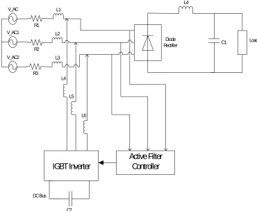
The shunt Active Filter generates currents to compensate for the un-desirable current components in the load current. For various non-linear loads in the power system, the input current quality can be polluted with harmonics. The Active Filters are used to supply the compensating harmonic requirements of the load allowing the supply current to be free of harmonics. (Akagi, Watanabe, & Aredes, 2007) The overview of the shunt Active Filter is shown in Figure 2.1.
The shunt active filter consists of a harmonic detector, current controller and an inverter. The inverter operates in a current regulated Pulse Width Modulated (PWM) mode. The harmonic detector is extracting the harmonics from the load current and shows what the compensator current should look like. The current controller produces the pulses for the inverter. And finally, the pulses fire the gates of the switches in the inverter to produce the compensating current.
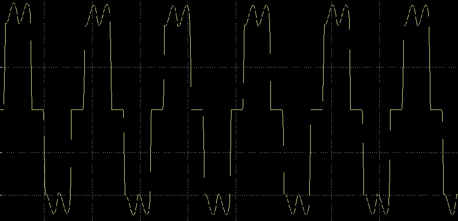
An open loop circuit is shown below in Figure 2.2. The waveform of the source current for this circuit is shown in Figure 2.3. The figure shows that the source current contains harmonics because of the load.
FIGURE 2.3 SOURCE CURRENT OF OPEN LOOP CIRCUIT
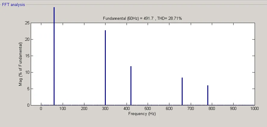
FIGURE 2.4 HARMONIC SCPECTRUM OF SOURCE CURRENT IN OPEN LOOP CIRCUIT
In order to precisely compensate for the high frequency harmonics, the bandwidth requirement of the inverter increases. To better compensate for these harmonics, the inverter requires a high switching speed.
FIGURE 2.5 CLOSED LOOP CIRCUIT (ACTIVE FILTER)
The waveform of the source current in the closed loop circuit is shown in Figure 2.6. Compared to Figure 2.3, the source current now contains much less harmonics with the presence of the Active Filter.
FIGURE 2.6 SOURCE CURRENT OF CLOSED LOOP CIRCUIT
The Harmonic Spectrum of this new source current is shown in Figure 2.7. The total harmonic distribution is now 2.64%. This complies with the IEEE 519 standard
FIGURE 2.7 HARMONIC SPECTRUM OF SOURCE CURRENT IN CLOSED LOOP CIRCUIT
The total distortion in the source decreased from 28.71% to 2.64% by the addition of the Active Filter to the Circuit. Thus, it can be seen that the Active Filter compensates for the harmonics from the load that would otherwise be polluting the source.
2.2
PQ THEORY
P-Q Theory is a well-known controller structure. In this section, the P-Q theory will be implemented on shunt active filters. P-Q Theory uses the measure values of the three phase voltages (ea, eb, ec) and three phase load currents (ia, ib, ic) to calculate the
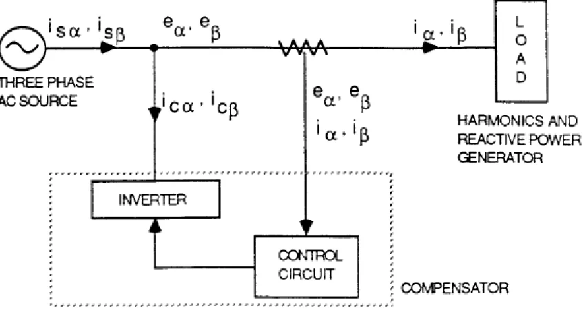
reference currents. There reference currents are used by the inverter to create the compensation currents. (Acharya) Figure 2.9 shows the diagram of a basic Active Filter compensator.
FIGURE 2.9 BASIC ACTIVE FILTER COMPENSATOR (ACHARYA)
orthogonal axes, αβ, system. After voltages and currents are transformed from abc to αβ, the instantaneous powers are defined on these coordinates. (Akagi, Watanabe, & Aredes, 2007)
The transformation from abc to αβ0 is done using the C matrix as shown below.
[
]
[
√ √
] [
]
[
]
[
√ √
] [
]
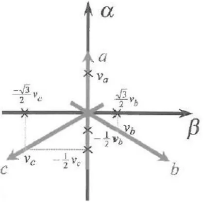
The abc axis shift to orthogonal αβ axes are shown below in Figure 2.10.
Figure 2.2.1 shows the two-phase currents of the source (
i
Sα, i
Sβ), load (i
α, i
β), and compensator (i
Cα, i
Cβ). The two-phase voltage (e
α, e
β), which is same for source and load, are also shown. From the diagram, it can be seen that:
Now, the instantaneous power components of the circuit will be examined on the αβ coordinates. The instantaneous real power P and the instantaneous imaginary power Q have dc and ac components:
Pdc is the average real active power consumed by the resistive nature of the load. Pac is
the oscillating real active power produced by the harmonics. Qdc is the average reactive
power consumed by the inductive, capacitive nature of the load. Qac is the oscillating
reactive power from the harmonics. (Acharya)
P and Q written in terms of the currents and voltages are given as:
[
] [
] [
]
So, from the previous equations, the following can be written:
[
] [
]
[
]
[
]
[
] [
]
Source Currents:
[
]
[
] [
]
where PS and QS are the powers consumed by the source.
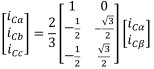
Active Filter Compensating Currents:
[
]
[
] [
]
where PC and QC are the powers consumed by the Active Filter.
In order for the active filter to serve as a harmonic compensator, the compensator must supply the oscillating active and reactive powers of the harmonics. So, Pc=-Pac and Qc
=-Qac.
[
]
[
] [
]
[
]
[
] [
]
[
]
[
] [
]
Since, Pc=-Pac and Qc=-Qac, then:
The source is only required to produce the DC components of the power, and the Active Filter will compensate for the harmonics present as shown above.
Now, the compensating currents to implement this harmonic compensator will be considered. (Acharya)
[
]
[
] [
]
[
] [
]
However, most common loads include a rectifier front-end (or diode bridge). For a diode bridge load, Pac is negligible in comparison to Qac as shown in Figure 2.11.
FIGURE 2.11 AC COMPONENTS OF P AND Q (ACHARYA)
So, if Pac is negligible, then the compensating currents are now:
[
]
[
] [
]
[
] [
]
[
]
[
√√
] [
]
This implementation of this PQ theory method is shown in its entirety in Figure 2.12.
FIGURE 2.12 PQ THEORY BLOCK DIAGRAM (ACHARYA)
2.2.1
MATLAB SIMULATIONS OF PQ THEORY
The PQ theory implementation shown above in Figure 2.12 was implemented in Matlab. In this section, the simulations of various signals in the implementation are shown.
FIGURE 2.13 THREE PHASE CURRENT
FIGURE 2.15 THREE PHASE VOLTAGE
FIGURE 2.16 TWO PHASE CONVERSION FOR VOLTAGE
FIGURE 2.17 SIGNAL Q
Figure 2.18 and Figure 2.19 show the two phase compensating currents, and signal that is calculated by the Active Filter.
FIGURE 2.19 SIGNAL
2.3
SERIES ACTIVE FILTER
FIGURE 2.20 BASIC SERIES FILTER (AKAGI, WATANABE, & AREDES, 2007)
The voltages on the current sources are VSa, VSb, and VSc. The load voltages are Va, Vb,
and Vc. And the compensating voltages are given as VCa, VCb, and VCc. The relationship
between these voltages is given as follows:
[
] [ ] [
]
The compensating voltages from the Active Filter are synthesized by 3 single-phase Voltage Source Inverters (VSIs). The reference voltages for these inverters are produced by the Active Filter Controller using the load voltages and currents. This calculation can be done using the P-Q theory implementation.
The real and imaginary powers, P and Q, are defined as follows:
Again, in order for the active filter to serve as a harmonic compensator, the
compensator must supply the oscillating active and reactive powers of the harmonics (Pc=-Pac and Qc=-Qac). Thus,
[
]
[
] [
]
[
] [
]
The two phase compensating voltages are converted back into three phase:
[
]
[
√ √] [
]
As show, series active filters uses voltages to compensate for the harmonics in the load as opposed to using current, the method used by shunt active filters.
2.4
SYNCHRONOUS REFERENCE FRAME
CONTROLLER
FIGURE 2.21 SYNCHRONOUS REFERENCE FRAME (SRF) CONTROLLER (BHATTACHARYA, FRANK, DIVAN, & BANERJEE, 1998)
The three phase load currents are . are the Active Filter
terminal voltages. The SRF controller consists of 3 sub-controllers: Positive Sequence SRF controller, Negative Sequence SRF controller, and DC Bus Voltage Controller. The Positive Sequence SRF controller extracts the harmonics in the synchronous d-q (direct-quadrature) reference frame. The Negative Sequence SRF controller extracts the
inverter DC bus. The fundamental frequency we are considering is 60Hz. (Bhattacharya, Frank, Divan, & Banerjee, 1998)
Positive sequence SRF
The Positive sequence SRF controller takes the three phase load currents and converts them into two phase load currents in terms of a stationary reference frame, ds-qs. This
stationary reference frame is then converted to a synchronous reference frame, de-qe,
using angle +θe. The currents in the synchronous reference frame are:
In the de-qe reference frame, the fundamental positive sequence components are DC
quantities, whereas all the harmonic components (mainly 5th and 7th harmonics) are AC
quantities. By passing through a low-pass filter with a cutoff around 200Hz, the dc component (fundamental positive sequence) can be isolated. Then, by subtracting this dc components from , the ac components, , are separated. The signals are converted back to the stationary
reference frame producing the harmonic components of the load current.
If a fundamental negative sequence is present, then the Positive sequence SRF
controller treats this as a harmonic because in the synchronous reference frame, this sequence will appear as an AC component (120Hz). The Negative sequence SRF controller will remove this sequence from the harmonic components found in the Positive sequence SRF. (Bhattacharya, Frank, Divan, & Banerjee, 1998)
Negative sequence SRF
The signals in the stationary reference frame, ds-qs, are then converted to a
synchronous reference frame, de-qe, using angle -θe. The currents in the synchronous
In the de-qe reference frame, the fundamental negative sequence components are DC
quantities, whereas all the harmonic components (mainly 5th and 7th harmonics) and
fundamental positive sequence are AC quantities. By passing through a low-pass filter with a cutoff around 200Hz, the fundamental negative sequence can be isolated. The extracted dc quantities are transformed back into the stationary reference frame. Then the fundamental negative sequence is subtracted from the output of the Positive sequence SRF controller.
Thus, this leaves just the harmonics signals in two phase (stationary reference frame). These signals are converted back to three phase as the final step. These reference currents, do not contain the fundamental negative sequence component.
This ensures that the active filter only compensates for the harmonics, and not the negative sequence current. (Bhattacharya, Frank, Divan, & Banerjee, 1998)
DC bus Voltage Controller
3
FIELD PROGRAMMABLE
ANALOG ARRAY
Field Programmable Analog Arrays (FPAA) are the analog counterpart of Field Programmable Gate Arrays (FPGA). Similar to FPGAs, FPAAs are reconfigurable and easy to design and simulate. This chapter gives background on FPAA and
AnadigmDesigner2 configuration tool.
3.1
OVERVIEW OF FPAA
FIGURE 3.1 FPAA DIAGRAM (ILA, BATTLE, CUFI, & GARCIA, 2002) (CIOC, LITA, VISAN, & BOSTAN, 2009)
There are two types of FPAAs: Discrete-time and Continuous-time. The internal structure of the CABs depends on the type of FPAA. Discrete-time FPAA is designed with switched capacitor technology, which is explained further in the next section. This allows for easier programmability of FPAA. Continuous-time FPAA is designed with transconductor technology. This is advantageous in terms of bandwidth, but it is limited in programmability.
3.2
SWITCHING CAPACITOR
TECHNOLOGY
Switched capacitor technology is utilized by Anadigm in its discrete-time FPAA chips. This technique is based on the fact that a capacitor switching between two circuit nodes at a certain frequency is equivalent to a resistor connecting these same nodes. This is shown in Figure 3.2. The resistance of this resistor depends on the capacitance and the switching frequency. (Cioc, Lita, Visan, & Bostan, 2009)
FIGURE 3.2 EQUIVALENCE OF SWITCHED CAPACITOR TO RESISTOR
When the switch is set to position S1, the capacitor is charged to the voltage V1, input voltage. The total charge on capacitor C is
.
When switch position is set to S2, the capacitor is now charged to voltage V2, output voltage. The total charge on capacitor C is now
.
V2 V1
V2 V1
S1 S2 R
The change in charge on capacitor C is given as
.
So, the current flowing from the input to output is
where T is the time between switching as shown in Figure 3.3.
FIGURE 3.3 TIMING DIAGRAM OF SWITCH POSITIONS
The frequency of switching can be found using T, where
The current flowing from input to output is the same for the equivalent resistor circuit. The voltage across the resistor is . Then, the resistance is
S1
S2
Therefore, as mentioned earlier, the resistance, , depends on the capacitance, , and the switching frequency, . (Dong, 2006)
By using switched-capacitors in place of resistors, the behavior of a resistor can be imitated except with higher accuracy, lower power consumption, and smaller area. Also, the value of the resistance can be changed by changing the switching frequency. Thus, using the switched-capacitor technology in the FPAA is beneficial technique.
3.3
FPAA ARCHITECTURE
FIGURE 3.4 AN231E04 CHIP AND EVALUATION BOARD (ANADIGMAPEX DPASP FAMILY USER MANUAL, AN 23X SERIES, 2005)
3.4
CONFIGURATION WITH ANADIGM
DESIGNER TOOL
Anadigm’s FPAA boards can be configured and reconfigured using AnadigmDesigner2 Tool. This software tool allows for a quick and easy way to
construct simple or complex analog circuit using a simple graphical interface. Design of the circuits in AnadigmDesigner 2 Tool is simple by selecting, placing, and wiring together built-in Configurable Analog Modules (CAM). CAMs are essentially small building blocks of a circuit including gains, filters, summations, multipliers, dividers, and rectifiers to name a few. (Priyadarshini, 2006)
Circuits constructed on AnadigmDesigner 2 Tool can be downloaded to the dynamically programmable Analog Signal Processor (dpASP) using an USB or RS232 cable. The dpASP can be modified as needed while operating. Once the new circuit data is loaded onto the dpASP completely, the configuration of the FPAA chip occurs in a single clock cycle. The FPAA chip can be reconfigured as many times as needed because the memory is SRAM based. (AnadigmApex dpASP Family User Manual, AN 23x series, 2005)
There are three regions of volatile SRAM within the dpASP device. These include Shadow SRAM, Configuration SRAM, and a Look-Up Table (LUT). The Shadow SRAM gets written to during configuration and reconfiguration. It holds the configuration data prior to the transfer of the data to the Configuration SRAM. Then, the Configuration SRAM controls the behavior of the analog signal processing circuitry. This transfer from the Shadow SRAM to the Configuration SRAM occurs in one clock cycle. The LUT
AnadigmDesigner 2 also includes a time domain functional simulator which shows the circuit’s behavior without an oscilloscope. Figure 3.6, Figure 3.7, and Figure 3.8 show aspects of the software discussed for a simple circuit. Figure 3.6 shows the circuit for implementing a sinusoidal function. The LUT for this function is shown in Figure 3.7. And Figure 3.8 shows the simulation result for the circuit.
FIGURE 3.7 LOOK-UP TABLE FOR SINUSOIDAL FUNCTION
Overall, the AnadigmDesigner 2 Tool allows for improved speed and ease of circuit design on the FPAA.
3.5
ADVANTAGES OF FPAA
Real world signals are analog, not digital. The use of FPAAs allows for the manipulations of these signals directly without the need for A/D or D/A conversion. This is because the FPAAs receive, process, and transmit these signals entirely in the analog domain. Also, the speed of the FPAA is suited for real time applications because of the lack of conversion. (Dong, 2006)
Another advantage of the FPAA chip is the speed of the design. FPAA circuits design is much faster than the conventional analog circuit design (draw, simulate, breadboard, and test). Using the AnadigmDesigner 2 software, it is simple to design a circuit and then configure an FPAA. And in seconds, the FPAA chip can be reconfigured to another circuit, if desired. This allows for much flexibility in the design while
4
FPAA IMPLEMENTATION
OF PQ THEORY
The PQ theory was implemented using four FPAA chips. The entire design as designed in AnadigmDesigner 2 is shown in Figure 4.1. First, the input, intermediate, and output signals will be considered for each individual chip. Then, the final output of the
implementation will be considered. The simulation results and experimental results will be compared for each of these signals to show that the experimental results are correct.
FIGURE 4.1 PQ THEORY DESIGN IN ANADIGMDESIGNER 2
4.1
INTERMEDIATE SIGNALS
4.1.1
CHIP 1
Figure 4.2 shows the circuitry of Chip 1 in AnadigmDesigner 2.
FIGURE 4.2 CHIP 1
Inputs:
Outputs:
FIGURE 4.3 SIMULATION RESULTS OF
Important signals from chip 1 include and . The simulation results and
experimental results of and are shown in Figure 4.4 and Figure 4.5. These two signals must be in quadrature as they are the two-phase conversions of the three-phase input. This characteristic does hold as can be seen in these figures.
FIGURE 4.5 EXPERIMENTAL RESULTS OF AND
The simulation results and experimental results of the output are shown in Figure 4.6 and Figure 4.7. Both figures show that is constant at the value of -1V.
4.1.2
CHIP 2
Figure 4.8 shows the circuitry of Chip 2 in AnadigmDesigner 2.
FIGURE 4.8 CHIP 2
Inputs:
Outputs:
Inputs to Chip 2 are the three phase current sources: . The simulation results and experimental results of these inputs are shown in Figure 4.9 and Figure 4.10. Also,
FIGURE 4.9 SIMULATION RESULTS OF INPUTS
FIGURE 4.10 EXPERIMENTAL RESULTS OF INPUTS
are also in quadrature, but this cannot be seen directly from the figures because of their unique shapes. Therefore, the signals are considered individually here.
FIGURE 4.11 SIMULATION RESULTS OF
FIGURE 4.13 SIMULATION RESULTS OF
FIGURE 4.14 EXPERIMENTAL RESULTS OF
FIGURE 4.15 SIMULATION RESULTS OF
4.1.3
CHIP 3
The design of Chip 3 is shown in Figure 4.17.
FIGURE 4.17 CHIP 3
Inputs:
Outputs:
FIGURE 4.18 SIMULATION RESULTS OF Q
4.1.4
CHIP 4
The design of Chip 4 is shown in Figure 4.20.
FIGURE 4.20 CHIP 4
Inputs:
Outputs:
(same as respectively)
FIGURE 4.21 SIMULATION RESULTS OF
FIGURE 4.23 SIMULATION RESULTS OF
4.2
FINAL OUTPUTS
This section reiterates the overall results of the PQ Theory implementation focusing on the inputs and outputs of the design in its entirety.
The inputs to the Active Filter Controller are the three phase currents and three phase voltages as shown in Figure 4.25.
The Active Filter Controller outputs the compensating reference currents, . The compensating currents have been left in two-phase because the predictive current controller only requires the two-phase currents to generate the pulses for the inverter. The Experimental outputs are given in Figure 4.26 and Figure 4.27.
FIGURE 4.26 OUTPUT OF ACTIVE FILTER CONTROLLER
5
C-RIO IMPLEMENTATION
OF PQ THEORY
The National Instruments C-RIO is a programmable automation controller that contains swappable industrial I/O modules. The C-RIO is powered by reconfigurable I/O (RIO) FPGA technology.
The C-RIO system consists of a reconfigurable chassis that contains the user-programmable FPGA, hot swappable I/O modules, and a real time controller. The chassis connects the controller and the I/O modules. Graphical LabVIEW software is used to program the FPGA.
The PQ theory was also implemented1 on the Compact-RIO (C-RIO). The LabVIEW
diagram of the implementation is shown in Figure 5.1 and Figure 5.2.
FIGURE 5.2 DIAGRAM OF PQ CONTROLLER IN LABVIEW
The outputs of from the C-RIO are shown in Figure 5.3. These results match with both the FPAA and Matlab Simulation Results. The delay of this implementation and the delay from the FPAA implementation will be compared in the following chapter.
6
COMPARISON OF
IMPLEMENTATIONS
To determine whether the FPAA implementation was indeed faster than its digital counterparts, the delays produced by each implementation will be compared.
The delays were measured by calculating the time difference between the zero crossings of two points (one point on the input signal, ,and the other on the output signal, ). These points were chosen because the zero crossings are ideally supposed
to coincide.
Figure 6.1 shows the delay in the implementation using C-RIO. Figure 6.2 shows the delay for the FPAA implementation.
FIGURE 6.2 DELAY IN FPAA IMPLEMENTATION
The delay for the C-RIO Implementation is 880µs. The delay in the FPAA
7
CONCLUSION
There is a need for Active Filter inverters to be switched at very high frequencies in order to match the harmonic requirement of the load. The next generation of Active Filters using Silicon Carbide (SiC) can achieve switching frequencies as high as 50-100KHz. For such devices, there is a need for a high speed controller which can be used to switch the inverter at these high speeds.
Current methods of designing Active Filter controllers include design of analog chips of using FPGAs and DSP. These methods involve much time in processing the signals.
REFERENCES
AnadigmApex dpASP Family User Manual, AN 23x series. (2005). Retrieved 2011, from
Anadigm, the dpASP company: http://www.anadigm.com/_doc/UM000231-U001.pdf
AN231E04 DataSheet. (2008). Retrieved 2011, from Anagidm, the dpASP company:
http://www.anadigm.com/_doc/DS231000-U001.pdf
Acharya, B. S. (n.d.). Realization of High Power Active Filter Network. MS Thesis. Madison, Wisconsin: University of Wisconsin.
Akagi, H., Watanabe, E. H., & Aredes, M. (2007). Instantaneous Power Theory and Applications to Power Conditioning. Hoboken, New Jersey, USA: John Wiley & Sons, Inc.
Bhattacharya, S., Frank, T. M., Divan, D. M., & Banerjee, B. (1998, September/October). Active Filter System Implementation. IEEE Industry Applications Magazine, 47-61.
Cioc, I. B., Lita, I., Visan, D. A., & Bostan, I. (2009). FPAA Implementation of Signal Processing Circuits for Radiation Sensors. 32nd International Spring Seminar on Electronics Technology (pp. 1-4). ISSE.
Dong, P. (2006). Design, Analysis and Real Time Realization of Artificial Neural Network for control and classification. PHD Thesis, North Carolina State University.
Raleigh, North Carolina.