BIST Hardware Synthesis for RTL Data
Paths Based on Test Compatibility Classes
Nicola Nicolici, Bashir M. Al-Hashimi, Andrew D. Brown, and Alan C. Williams
Nicola Nicolici
Bashir M. Al-Hashimi
Andrew D. Brown
Alan C. Williams
Electronic Systems Design Group
Department of Electronics and Computer Science
University of Southampton
Southampton SO17 1BJ
U.K.
Contact address:
Dr. Bashir M. Al-Hashimi
Electronic Systems Design Group
Department of Electronics and Computer Science
University of Southampton
Southampton SO17 1BJ
U.K.
Tel: +44-23-8059-3249
Fax: +44-23-8059-2901
Email: [email protected]
A short and preliminary version of this work is published in:
BIST Hardware Synthesis for RTL Data
Paths Based on Test Compatibility Classes
Abstract
New BIST methodology for RTL data paths is presented. The proposed BIST methodology
takes advantage of the structural information of RTL data path and reduces the test application
time by grouping same-type modules into test compatibility classes (TCCs). During testing,
compatible modules share a small number of test pattern generators at the same test time leading
to significant reductions in BIST area overhead, performance degradation and test application
time. Module output responses from each TCC are checked by comparators leading to
substan-tial reduction in fault-escape probability. Only a single signature analysis register is required to
compress the responses of each TCC which leads to high reductions in volume of output data
and overall test application time (the sum of test application time and shifting time required to
shift out test responses). This paper shows how the proposed TCC grouping methodology is a
general case of the traditional BIST embedding methodology for RTL data paths with both
uni-form and variable bit width. A new BIST hardware synthesis algorithm employs efficient tabu
search-based testable design space exploration which combines the accuracy of incremental test
scheduling algorithms and the exploration speed of test scheduling algorithms based on fixed
test resource allocation. To illustrate TCC grouping methodology efficiency, various
bench-mark and complex hypothetical data paths have been evaluated and significant improvements
1
Introduction
Register transfer-level (RTL) is the abstraction level in the behavioral domain of the very large
scale integration (VLSI) design flow where an integrated circuit is seen as sequential logic
con-sisting of registers and functional units that compute the next state given the current memory
state. The functional units which compute the next state logic are arithmetic logic units (ALU),
multipliers or complex multi-functional library modules. The complexity of modern digital
cir-cuits requires automated synthesis and optimization techniques that can explore a wide class of
implementations choices using computer-aided design (CAD) tools [1]. High level-synthesis is
the process of generating RTL structure from a behavioral description [2]. The modules
(func-tional units) allocated by high level synthesis algorithms are generated by module generators
which are able to synthesize the layout of modules with high performance and device density.
The modules are placed in module libraries and have identical physical information. Given the
complexity of modern digital circuits it is necessary that testability is addressed at RTL due to
fewer elements than at the gate level which makes test synthesis and test scheduling problems
more tractable.
1.1
Previous work
Two main approaches have been proposed to enhance the testability of digital circuits at RTL.
The first approach is aimed at minimizing the complexity of automatic test pattern generation
(ATPG). In [3] the complexity of ATPG for scan-based design for testability (DFT) techniques
is reduced by an efficient selection of scan flip-flops using RTL information. The high test
application time associated with scan-based technique is overcome by using scan chain
recon-figuration to reduce shifting time [4] and use of partial scan design of RTL circuits [5]. However,
a significant disadvantage of the scan-based technique is that at-speed testing with the complete
test set is not possible (i.e., all test patterns cannot been applied at the operational speed of the
circuit). To solve at-speed testability, nonscan DFT techniques applicable to RTL data paths
were proposed in [6]. Instead of selecting flip-flops to make controllable/observable as the
con-ventional scan-based techniques, execution units are selected using an execution unit graph.
Performing at-speed testability and reducing test area overhead is achieved at the cost of
expen-sive test pattern generation phase. To reduce the costs of test pattern generation, an algorithm
that adds minimal test hardware in order to ensure that all the embedded modules in the circuit
are hierarchically testable was presented in [7]. In [8] a technique for extracting functional
use of high level information [7]. Recently in [9] a testability analysis methodology for modular
designs is introduced which extracts a set of justification and propagation requirements based
on the cone-of-logic of each input and output. However, despite reducing both area overhead
and ATPG complexity the test application time and the volume of output data are still high.
The second approach to enhance testability of RTL circuits is built-in self-test (BIST) [10].
While scan BIST [11] eliminates the use of ATPG, it still requires high test application time
and volume of output data associated with scan based design. On the other hand parallel BIST
reduces both test application time and volume of output data [10]. From now onwards BIST
hardware synthesis refers to parallel BIST test hardware insertion for RTL data paths. BIST
hardware synthesis at RTL can be further subdivided to functional-based and structural-based
BIST hardware synthesis. Functional-based BIST hardware synthesis based on algorithmic and
deterministic BIST scheme was presented in [12].This algorithm uses a high-level cell fault
model, and data paths are assumed to be composed of only specific adders/subtracters and
multipliers. Combination of different BIST schemes and reusing pre-existing modules of the
data path for functional-based BIST hardware synthesis under heterogenous test schemes was
proposed in [13]. Another functional-based BIST hardware synthesis [14] uses the controller
netlist to extract the test control/data flow to derive a set of symbolic justification and
propa-gation paths. In [15] regular expression based high level symbolic testability analysis further
reduces test area overhead under delay constraints by carefully carefully selecting a small subset
of registers to serve as test pattern generators and output response analyzers. Recently,
redun-dancy identification and testability improvement of digital filter data paths was proposed in [16]
which restricts to circuits which are described as a network of shift, add, delay, sign-extension
and truncation elements. All the previous functional-based BIST hardware synthesis techniques
[12–16] depend strongly on the functional information of data path modules and/or high level
control/data flow. On the other hand, structural-based BIST hardware synthesis inserts test
registers by analysing interconnections between registers and modules in a given RTL netlist,
without using the functional information of data path modules or high level control/data flow.
This makes structural-based BIST hardware synthesis more suitable at RTL than
functional-based BIST hardware synthesis when only the structural interconnection of data path modules
and registers is given. An early structural-based BIST hardware synthesis algorithm at RTL
was presented in [17] without taking into account the test application time. Another
structural-based BIST hardware synthesis algorithm that minimizes test application time and BIST area
overhead was proposed in [18]. The algorithm, however, has an inefficient testable design space
before the test scheduling process. Furthermore, the optimization algorithm limits the number
of test plans to only four per module, leading to limited number of explored testable designs.
To overcome the fixed test resource allocation, simultaneous test hardware insertion and test
scheduling was proposed in [19]. While previous test scheduling algorithms [20–22] assumed
fixed test resource allocation, the work in [19] presented an incremental test scheduling
proce-dure which overcomes the limited testable design space exploration encountered with fixed test
resources. Despite its good performance, the algorithm in [19] is not capable of dealing in low
computational time with complex designs such as 32-point discrete cosine transform (DCT),
since a branch and bound-based algorithm is employed to explore the testable design space. A
recent approach which explores the testable design space during high level synthesis has been
proposed in [23]. However, same test length is considered for all data path modules which leads
to unnecessary long test application time.
1.2
Motivation and objectives
Up to this point, the described structural-based BIST hardware synthesis algorithms have
as-sumed the BIST embedding methodology where every module port is embedded between a test
pattern generator and a signature analysis register. This methodology is inefficient due to the
following four problems:
a. to achieve low test application time high number of test registers is required which leads
to large BIST area overhead and performance degradation.
b. since every module belongs to a different BIST embedding the aliasing can occur for
every module tested separately leading to increase in fault escape probability for the entire
data path.
c. the increased number of signature analysis registers yields large volume of output data
and increases the overall test application time due to the time required to shift out of test
responses.
d. the huge size of the testable design space where test synthesis and test scheduling are
strictly interrelated leads to long computational time for efficient testable design space
exploration.
To overcome the large number of test registers in the BIST embedding methodology
(prob-lem a), a methodology based on chaining modules into test paths was described in [24, 25].
test path generation and test scheduling. Despite reducing the performance degradation, the
great number of test patterns for each test path, which are no longer truly pseudorandom,
in-creased the test application time. The test path generation algorithm lacked the global view of
the design space and the suboptimal solution depends on the order in which the modules are
processed. Furthermore, the pipelined test scheduling for multiple clock cycles test paths
in-creases the complexity of the BIST controller as the design complexity is enlarged. Concurrent
checkers [27, 28] have been used for reducing fault escape probability (problem b) during
off-line self-test. While large BIST area overhead solutions based on duplicate circuitry realized
in complementary form are described in [27], the results presented in [28] show that extra test
hardware required to achieve low fault-escape probability, if designed as a combination of a
concurrent checker and signature analysis registers, is more cost-effective than the design using
only signature analysis registers. Recently a different approach which combines mutual and
signature testing schemes [29] has been proposed for reducing fault escape probability. This
approach uses test registers that combine equality comparators and signature analysis registers
leading also to reduction in the volume of output data (problem c). However, due to large
number of test registers when maximum test concurrency is targeted the problem of BIST area
overhead and performance degradation are not solved. The previous approaches [24–29]
pro-posed separate solutions for solving only one of the problems (a) - (c) at the expense of the
other problems of the BIST embedding methodology. Furthermore, the interrelation between
test synthesis and test scheduling which leads to huge size of the testable design space (problem
d) was not solved efficiently by the previously described approaches [17–22] which trade-off
the quality of the final solution and computational time.
The aim of this paper is to introduce a new BIST methodology for RTL data paths using
a new concept called test compatibility classes which reduces test application time with
com-parable or even lower BIST area overhead when compared to the traditional BIST embedding
methodology. The proposed BIST methodology which targets data flow intensive application
domains, like digital signal processing, communications and graphics, overcomes the
perfor-mance degradation, fault-escape probability and volume of output data associated with the BIST
embedding methodology. Furthermore efficient heuristics for testable design space exploration
produce high quality of the final solution in low computational time. The paper is organized
as follows. Section 2 introduces the TCC grouping methodology. BIST hardware synthesis for
TCC grouping is given in section 3. Experimental results of benchmark and complex
hypo-thetical data paths are presented in section 4. Finally, concluding remarks are given in section
2
New BIST methodology for RTL data paths
This section motivates the key ideas presented in this paper through examples and gives
for-mal concepts and definitions of the proposed BIST methodology. First the shortcomings of
the traditional BIST embedding methodology are identified and benefits of the proposed BIST
methodology are outlined using a detailed example. Then the formal definition of test
compati-bility classes is given.
2.1
An illustrative example
Traditional BIST embedding methodology embeds every module port between a test pattern
generator and a signature analysis register. This may lead to conflicts between different test
resources when maximum test concurrency is targeted. Furthermore the number of test
re-sources for low test application is extremely high leading to both high BIST area overhead and
performance degradation. The proposed BIST methodology takes advantage of the structural
information of RTL data path and reduces the test application time by grouping same-type
mod-ules into test compatibility classes (TCCs). Two modmod-ules are of the same type if they are two
different instances of the same module library prototype and hence they have the identical
phys-ical and structural information. Due to the identphys-ical physphys-ical and structural information the fault
sets of two same-type modules have the same detection probability profile [30]. Thus, the same
test pattern generators can be used simultaneously (no need to schedule the tests at different test
times) for two or more same-type modules without decreasing the fault coverage. On the other
hand fault sets of different-type modules have different detection probability profiles and hence
different test pattern generators and different test application times are needed to satisfy the
required fault coverage. It should be noted that use of hard macro implementations of library
modules which have identical physical and structural information can significantly improve the
final design [31]. Furthermore design methodologies which use regular elements and identify
similarity need to be incorporated in state of the art CAD tools [31, 32]. Therefore the proposed
BIST methodology is targeting design flows that use few pre-designed module types with
iden-tical physical and structural information and exploits the regularity of the data path to reduce
test application time and BIST area overhead as explained in the following example.
Example 1 To give insight of the proposed BIST methodology consider the simple data path
shown in Figure 1(a). The data path has 3 modules of module-type Atypeand 9 registers. Each
module is annotated with its name (A1-A3). In order to test all the modules in a single test
multiple-input signature registers (MISRs). Each test pattern generator (LFSR1-LF SR6) applies test
pat-terns to each input port of every module and each signature analysis register (MISR7-MISR9)
evaluates the output responses of every module. The paths from test pattern generators to
mod-ule input ports through multiplexers are denoted by dotted lines. In order to test all the modmod-ules
simultaneously 6 LFSRs and 3 MISRs are required. Note the number of 2-to-1 multiplexers in
the data path is 4 and hence there are 24paths to apply test patterns to module input ports. Any
other configuration of test registers which implies sharing of a test resource in order to reduce
BIST area overhead will lead to an increased number of test sessions and hence test application
time. However, if Atype modules are instances of the same module library prototype, then they
have identical physical and structural information and hence identical detection probability
pro-file. Thus if test patterns are applied to modules A1 A3simultaneously same fault coverage is
achieved when compared to applying test patterns in different test sessions. Note that LFSR1is
the only test register which applies test patterns to left input port of module A1and is connected
to left input ports of A2 and A3. If multiplexers at left input ports of A2and A3select LFSR1as
shown in Figure 1(b), the test registers LFSR3and LFSR5 (Figure 1(a)) are unnecessary. This
clearly leads to savings both in BIST area overhead and performance degradation, since
regis-ters R3and R5(Figure 1(b)) are not modified to perform test functions. Similarly if multiplexers
at right input ports of A1and A2select LFSR6(Figure 1(b)), the test registers LFSR3and LFSR5
are unnecessary. When same test patterns are generated by LFSR1 and LFSR6 at input ports
of A1, A2, and A3 same output responses are expected at the same time. Hence a comparator
CA is used to check the output responses. Only a single signature analysis register MISR7 is
allocated to compress the output responses of all the modules A1,A2, and A3 which are tested
simultaneously. The signature analysis register MISR7is necessary to detect faults in the case
when output responses of all the three modules A1,A2, and A3 are equal during the entire test
application period but different from the fault-free output response. The use of comparators to
check the output responses of all the same-type modules tested concurrently solves three
prob-lems. Firstly it reduces both BIST area overhead (1 MISR and 1 comparator vs. 3 MISRs) and
performance degradation (1 MISR vs. 3 MISRs embedded in data path). Secondly it reduces
fault-escape probability since faulty output responses which map into fault-free signatures in
the BIST embedding methodology will be detected by the comparators. And thirdly, the
num-ber of signatures is reduced which has the following two implications. On one hand the volume
of output data is reduced which leads to less storage required for test data. On the other hand
the overall test application time is reduced due to less clock cycles needed to shift out the test
out the output response stored in MISR7, MISR8, and MISR9 (Figure 1(a)) is 24 clock cycles
when compared to only 8 clock cycles required to shift out the output response stored in MISR7
(Figure 1(b)).
Solutions using comparators described in [27] to enhance fault escape probability are based
on duplicate circuitry realized in complementary form leading to huge BIST area overhead. The
proposed BIST methodology is fundamentally different where no duplicate circuitry is required
and comparators are checking the responses of same-type modules which are instances of same
module prototype. This makes the proposed BIST methodology suitable for complex data paths
with high number of same-type modules generated automatically by modern CAD tools. The
goal of the proposed BIST methodology is to test all the modules of the data path which are
random pattern resistant and present testability problems. A part of the steering logic and
inter-connections are tested for free while testing the modules. It is known that a set of four vectors
is sufficient to test a 2-to-1 multiplexer of any bit width. Similarly the functional registers are
C-testable and non random pattern resistant structures. The comparators are the only extra DFT
hardware added for BIST purposes. Approximately 2
n
k test patterns are required to test a
n-input k-bit comparator. Any portion of the data path not tested by the proposed BIST
method-ology is tested using a small global set of functional patterns. Since comparators check the
responses of same-type modules which are inherently different cones-of-logic the small global
test of functional patterns can be generated easily using the justification/propagation techniques
[8, 9]. The small global set of functional patterns is applied in a preliminary phase and has no
impact on the overall test application time.
2.2
Definition of Test Compatibility Classes
An RTL data path consists of nreg registers, nmod two-input modules of nres module-types, and
multiplexers. Before test compatibility class concept is introduced, it is necessary to present the
following preliminary definitions.
Definition 1 A test register Rx performs the test pattern generation function (TPGF) for input
port k (IPk) of module Ma if test patterns for IPk of Ma are provided by Rx. Let IRS
MaIPk
denote the set of registers that are connected to IPk of Mathrough only multiplexers. One and
only one test register from IRS
Ma IPk is performing TPGF for IPkof Ma.
The test registers used to perform TPGF are: LFSRs, built-in logic block observers (BILBOs)
and concurrent BILBOs (CBILBOs). If for each input port l (IPl) of every data path module,
l 12
patterns to data path modules is 2 nmod
∏
l 1
ml. The testable data paths where both input ports of
a module receive same test patterns are not valid in the proposed BIST methodology due to
the correlation between identical test patterns at both input ports which leads to a substantial
decrease in fault coverage.
Definition 2 Two same-type modules, Maand Mb, are incompatible, i.e. they cannot be tested
simultaneously, if there is a test register Rx that performs TPGF for input port 1 (IP1) of Ma
and input port 2 (IP2) of Mb, or if there is a test register Rythat performs TPGF for IP2of Ma
and IP1 of Mb. Two different-type modules are incompatible if there is a test register Rz that
performs TPGF for any input port of Maand any input port of Mb. Two modules are compatible
if they are not incompatible.
Having described test module incompatibility, now the formal definition of test compatibility
classes is given.
Definition 3 A test compatibility class TCCij (i is called the class index, while j is called the
module-type index) is a set of modules that satisfies the following three properties:
i. all the modules from TCCijare compatible and belong to the same module-type j
ii. two test compatibility classes, TCCpj and TCCq
l, are incompatible if for at least one
module Ma from TCCpj there exists at least one module Mb from TCCql such that Ma
and Mbare incompatible.
iii. modules from TCCij are tested simultaneously by same test patterns and the output
re-sponses are checked by an n-input k-bit comparator, where n is the cardinality of TCCij
and k is the bit-width of the data path. A single signature analysis register compresses
the output response of a single module from TCCij to verify that the output response
sequence is correct.
The first property of TCCs (Definition 3-(i)) guarantees that all the modules from a TCC can
share test pattern generators leading to less BIST area overhead and performance degradation,
without any penalty in test efficiency or test application time. The second property of TCCs
(Definition 3-(ii)) indicates that high number of incompatible modules should be merged in a
small number of incompatible TCCs leading to maximum test concurrency and hence reduction
in test application time. The use of comparators described in the third property of TCCs
signature analysis registers leads to smaller volume of output data and overall test application
time (the sum of test application time and shifting time required to shift out test responses). Let
ORS
Mk denote the set of registers that are connected to the output of module Mkthrough
mul-tiplexers only. The output register set of TCCij, ORS(TCCij), is the union of output register
sets of all the modules from TCCij. The signature analysis register for TCCijis chosen from
ORS(TCCij). The test registers used for signature analysis are MISRs, BILBOs and
CBIL-BOs. The number of highly expensive CBILBOs required for testing the self-loops in the data
path is reduced when using the proposed methodology due to the greater number of potential
signature analysis registers for each TCC. While the traditional BIST embedding methodology
has nmod signatures, the proposed BIST methodology has only nres
∑
j 1
nclasses
j signatures, where
nclasses
j is the number of classes for module-type j. When nmod = nres every module is an
instance of a different module library prototype and according to Definitions 1-3 the proposed
TCC grouping methodology is identical with the traditional BIST embedding methodology
for RTL data paths. Hence, the BIST embedding methodology is a particular case of the TCC
grouping methodology when each TCC consists of a single module.
The proposed TCC grouping methodology is not limited to only uniform bit width data
paths. Same-type modules which belong to a TCC have the same bit width. However different
module types can have different bit width which does not imply any change in the methodology.
Definitions 1-3 hold for variable bit width data paths. In the variable bit width case TCCs
of different bit width are tested using different bit-width for test registers and n-input k-bit
comparators. Moreover, the proposed methodology can handle both several modules chained
together without any registers between them and particular cases when logic/RTL synthesis
tools transform different instances of the same module type into different implementations by
considering them as new module-types with new detection probability profile.
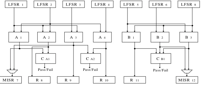
Example 2 To illustrate Definitions 1-3 consider the data path example of Figure 2, where
LFSR1, LFSR2, LFSR3and LFSR4test four modules of Atype, and LFSR5, LFSR6 and LFSR7
test three modules of Btype. LFSR1 generates test patterns for input port 1 (IP1) of A1 and A2
and for input port 2 (IP2) of A3. LFSR2 generates test patterns for the IP2of A1and A2and for
IP1 of A4. LFSR3generates test patterns for IP1of A3 whilst LFSR4provides test patterns for
IP2 of A4. Modules A1 and A2 belong to TCC00 (class index is 0 and Atype index is 0). Due
to incompatibilities between A1 and A3 and between A2and A4, modules A3and A4belong to
TCC10 (class index is 1). Similarly, modules B1, B2 and B3 are all compatible and belong to
output responses of modules from TCC00 are compared by a 2-input 8-bit comparator (CA1).
Similarly, the output responses of modules from TCC10are compared by another 2-input 8-bit
comparator (CA2). On the other hand, output responses of modules from TCC01are compared
by a 3-input 8-bit comparator (CB1). If any error occurs during testing, the Pass Fail signal
will be activated and the testing process will stop. The output register set ORS(A1) is R7 , the
ORS(A2) is R8
, the ORS(A3) is
R7, R9
and the ORS(A4) is R10
. Hence the ORS(TCC00)
is R7
R8 and the ORS(TCC10) is R7
R9 R10 . Similarly, the ORS(TCC01) is R11
R12 .
Any of these two registers R11 and R12 can be configured as signature analysis register for
TCC01. The procedure that chooses the best signature analysis register is presented in section
3.3. For data path example in Figure 2 the chosen signature analysis register for TCC01is R12
whilst both TCC00and TCC10use R7as signature analysis register at different test times.
3
New BIST hardware synthesis algorithm for TCC
group-ing
Having described the TCC grouping methodology, now a BIST hardware synthesis algorithm
is considered. As outlined in section 2, the BIST embedding methodology is a particular case
of the TCC grouping methodology where each TCC consists of a single module. Therefore,
testable design space for the TCC grouping methodology is much larger and more complex
than testable design space for the BIST embedding methodology. The previous approaches [17–
22] which trade-off the quality of the final solution and the computational time are unsuitable
for the size and complexity of the TCC grouping methodology. This section presents a new
and efficient testable design space exploration which combines the accuracy of incremental
test scheduling algorithms [19] with the exploration speed of test scheduling algorithms based
on fixed test resource allocation [20–22]. Section 3.1 outlines the general framework of tabu
search-based testable design space exploration. Section 3.2 presents the generation of new
solutions and speed up techniques for local neighborhood search. Finally in section 3.3 an
incremental TCC scheduling algorithm for each solution is proposed.
3.1
Tabu search-based testable design space exploration
Tabu search [33] was proposed as a general combinatorial optimization technique. Tabu search
falls under the larger category of move-based heuristics which iteratively construct new
candi-date solutions based on the neighborhood that is defined over the set of feasible solutions and
how one solution is transformed into another solution in a single step. The philosophy of tabu
search is to derive and exploit a collection of principles of intelligent problem solving. Tabu
search controls uphill moves and stimulates convergence toward global optima by maintaining
a tabu list of its r most recent moves, where r is called tabu tenure and it is a prescribed
con-stant. Occasionally, it is useful to override the tabu status of a move when the move is aspirated
(i.e., improves the search and does not produce cycling near a local minima). Tabu search based
heuristics are simple to describe and implement. Furthermore, a well defined cost function
and the use of topological information of the design space will lead to an intelligent search of
high quality solutions in very low computational time. Before the proposed tabu search-based
testable design space exploration is described, it is necessary to present the following definition.
Definition 4 A solution in the testable design space is a partially testable data path PT-DP
where test pattern generators are allocated for each data path module. A fully testable data path
FT-DP is generated by allocating signature analysis registers for each test compatibility class
of the partially testable data path.
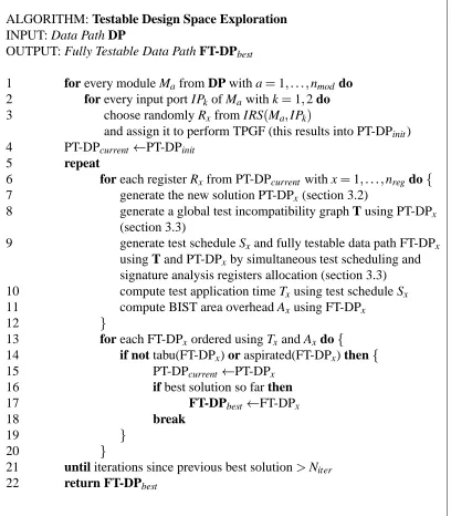
The proposed tabu search-based testable design space exploration is summarized in Figure 3.
The algorithm starts with an initial solution which is a partially testable data path PT-DPinit
obtained by randomly assigning a single test pattern generator to each input port of every
mod-ule from the data path as shown from lines 1 to 4. During the optimization process (lines 5 to
21) for each current solution PT-DPcurrent, a number of nreg neighbor solutions are generated
as described in section 3.2. Test application time Tx and BIST area overhead Ax are computed
after a fully testable data path FT-DPxand a test schedule Sxare generated using the algorithms
from section 3.3, as shown from lines 8 to 12. The optimization process is guided towards the
objective of minimal test application time design by a cost function which is defined as follows.
Definition 5 The cost function is a 2-tuple Cx
Tx Ax), where Tx is the test application time,
Axis the BIST area overhead and the following relations are defined:
i. Cx1 Cx2if (Tx1 Tx2) and (Ax1 Ax2)
ii. Cx1 Cx2if (Tx1 Tx2) or (Tx1
Tx2and Ax1
Ax2)
iii. Cx1 Cx2if (Tx1 Tx2) or (Tx1
Tx2and Ax1
Ax2)
The main objective of the cost function is test application time with BIST area overhead used
should be noted that the minimization of other parameters outlined in section 2, performance
degradation, volume of output data, overall test application time and fault escape probability, is
a by-product of the proposed optimzation using the previously defined cost function. Based on
the value of the cost function and on the tabu status of a move, a new solution is accepted or
rejected as described from lines 14 to 19 in Figure 3. The tabu list contains registers involved in
a move as described in section 3.2. A move is classified as tabu if a register involved in the move
is present in the tabu list. The tabu tenure (length of the tabu list) varies from 5 (small designs)
to 10 (complex designs). A move is aspirated as shown in line 14 if it has produced a solution
which is better than the best solution reached so far. The testable design space exploration
continues until the number of iterations since the previous best solution exceeds a predefined
Niter.
3.2
Generation of new solutions and speed up techniques for local
neigh-borhood search
The neighborhood of the current solution in the testable design space PT-DPcurrent is defined
with nreg feasible neighbor solutions. For each data path register there is a single neighbor
so-lution. Each of the nregsolutions is provided by an independent subroutine designed to identify
better configuration of test registers based on two new metrics. Due to the huge size and
com-plexity of the testable design space, speed up techniques for efficient exploration are required.
Before defining the neighbor solution for each register two new metrics and a theorem used for
reducing the testable design space are presented.
Definition 6 The current spatial sharing degree CSSD
Rx j IPk
of register Rx for input port
k (IPk) of module-type j is the number of modules of j for which Rx performs test pattern
generation function (TPGF) for IPk in the current partially testable data path.
Definition 7 The maximum spatial sharing degree MSSD
Rx j IPk of register Rxfor input port
k (IPk) of module-type j is the number of modules of j for which Rxcan perform TPGF for IPk.
The value of MSSD
Rx jIPk is the cardinality of the set of modules of module-type j whose
IPk is connected to Rx through only multiplexers.
The following theorem presents a very important theoretical result which has two implications
on speeding up local neighborhood search. See [34] for the proof.
Theorem 1 Consider two current solutions, PT-DP1current and PT-DP2current, with different CSSD
Rx j IPk
for given Rx, j and IPk. In PT-DP
1
CSSD
Rx j IPk
MSSD
Rx j IPk
, whilst in PT-DP
2
current the current spatial sharing degree is
CSSD
Rx j IPk
MSSD
Rx j IPk . Then PT-DP
2
current has at most the number of TCCs as
PT-DP1current.
The first implication of the theoretical result of Theorem 1 reduces the total testable design
space to the representative testable design space. The total testable design space consists of
partially testable data paths with all the possible values 0 CSSD
Rx j IPk
MSSD
Rx j IPk
such that all the modules are assigned one and only one test pattern generator. The
represen-tative testable design space consists of partially testable data paths for which CSSD
Rx j IPk
is considered only MSSD
Rx j IPk such that all the modules are assigned one and only one
test pattern generator. Consider the simple data path of Figure 1. In the first case when the
current spatial sharing degree for R1is CSSD
R1 AtypeIP1
1 two more test registers LFSR3
and LFSR5 are necessary to generate test patterns for IP1 of modules A2 and A3 as shown in
Figure 1(a). On the other hand when CSSD
R1Atype IP1
MSSD
R1Atype IP1
3 only one
test pattern generator is necessary to generate test patterns for IP1 of all the three modules as
shown in Figure 1(b). The case when CSSD
R1Atype IP1
1 has greater BIST area overhead
and performance degradation due to LFSR3 and LFSR5. Furthermore if the simple data path
of Figure 1 is a small part of a more complex data path, where LFSR3and LFSR5are already
allocated to perform TPGF for different module-types, assigning LFSR3and LFSR5to perform
TPGF for IP1 of A2 and A3 respectively, will introduce conflicts between test resources
lead-ing to incompatible modules and hence increase in test application time. Theorem 1 justifies
the reduction of the total testable design space where all the CSSD
R1 AtypeIP1 0
1 2 3
are examined in the search of feasible partially testable data paths to the representative testable
design space where only CSSD
R1 AtypeIP1
3 is considered.
The second implication of the theoretical result of Theorem 1 is concerned with efficient
generation of moves in the representative testable design space. Generation of a move in the
testable design space for register Rxconsists of two phases:
i. The first phase computes: x
j IPk
MSSD
Rx jIPk CSSD
Rx jIPk ;
xis a metric
that measures the difference between the potential and actual use of Rx as a test pattern
generator for IPkof j modules. Note there are 2
nresvalues of x for each register Rx.
ii. In the second phase the move for Rx that has the maximum value of max is chosen. If
there are two or more jmand/or IPkn for which x
jm IPkn
max the move for jmand
IPkwith the maximum value of MSSD
Let jmaxbe the index of module-type and kmaxbe the index of input port for which maxis
max-imum. Let M1
Mn be the set of modules of module-type jmax whose IPkmax is connected
to Rxthrough only multiplexers. Before the move, Rx performs TPGF for M1
Mt , whilst Ry
1 Ry2
Rym perform TPGF for Mt
1
Mn . After the move, Rx performs TPGF for M1
Mn , whilst CSSD
Ryi jmax IPkmax are decreased, with i
1 m. The previously
de-scribed two phases are repeated for each data path register and hence a neighborhood of nreg
feasible solutions is generated. Increasing the current spatial sharing degree of the selected test
registers leads to a smaller number of test pattern generators and hence reductions in BIST area
overhead and performance degradation. Furthermore, the number of incompatibilities between
TCCs is decreased which leads to lower test application time. Moreover the most important
fea-ture of the local neighborhood search is the speed up technique for efficient exploration caused
by reduction in the size of the testable design space to be explored.
3.3
Incremental TCC scheduling algorithm
So far the testable design space to be explored was reduced with respect to the number of test
registers required for test pattern generation using the speed up techniques for local
neighbor-hood search. The algorithms outlined in this section further shrink the size of the testable design
space by considering simultaneous TCC scheduling and signature analysis registers allocation
for each partially testable data path generated by local neighborhood search. Firstly the
assign-ment of every data path module to test compatibility classes to maximize test concurrency is
summarized. Secondly the algorithm for simultaneous TCC scheduling and signature analysis
registers allocation is described.
To achieve maximum test concurrency it is required that a large number of different-type
test compatibility classes are compatible. Following the second property of TCCs (Definition
3-(ii)) a high number of incompatible modules are sought to be merged in a small number of
in-compatible TCCs. This will reduce the number of edges in the global test incompatibility graph
which is defined as follows. A global test incompatibility graph (G-TIG) is a graph where a
node appears for every TCC and an edge exists between nodes if test compatibility classes are
incompatible. All the edges from G-TIG belong to the edge set E. The generation of G-TIG
is carried out in three steps. The first step assigns incompatible same-type modules into test
compatibility classes and generates the initial G-TIG. Data path modules that are incompatible
with different-type modules are considered in the second step. Unassigned data path modules
are assigned to the already existing TCCs such that the number of incompatibilities between
unas-signed modules which are compatible with all TCCs are added to TCCs such that an increase
in the output register set (ORS) of each TCC is achieved. This reduces the number of conflicts
between signature analysis registers that are allocated during the test scheduling process
lead-ing to lower test application time. The proposed algorithm for generation of G-TIG guarantees
by construction that every module is assigned to a TCC and the number of nodes and edges in
G-TIG is minimum. This implies maximum test concurrency of the partially testable data path
which is a good starting point for the incremental test scheduling algorithm.
Test scheduling is performed using the global test incompatibility graph described
previ-ously. Fault sets of different-type modules have different detection probability profiles as
out-lined in section 2.2. Hence, TCCs of different module-types need different test application
times to satisfy the required fault coverage. Thus, the TCC scheduling algorithm deals with
unequal test lengths. The test scheduling algorithm for partitioned testing with run to
comple-tion from [20] needs to be modified such that test scheduling and signature analysis registers
allocation is done simultaneously. Unlike the algorithm 2M from [20] which schedules tests
for a fixed test resource allocation and thus leading to inefficient design space exploration, the
proposed algorithm simultaneously schedules TCCs and allocates signature analysis registers.
This leads to both more efficient testable design space exploration and higher test concurrency
since conflicts between signature analysis registers are avoided. In order to clarify the
neces-sary modifications two more notations are introduced: U is the set of used test registers that
have compressed output responses at a previous test time and B is the set of busy test registers
that are compressing output responses at the current test time. The following three necessary
modifications are carried out to algorithm 2M from [20] in order to perform simultaneous TCC
scheduling and signature analysis register allocation.
i. if all the registers in ORS
TCCij are busy at the current test time then test TCCij is
removed from the candidate node set being postponed for a later test time; otherwise for
every available register Rk in ORS
TCCij , it is checked whether Rkbelongs to the used
test register set and the Rk with the maximum fanin is chosen; this choice will allow Rk
to be reused at a later test time.
ii. when the shortest currently active test TCCij is completed, the test register Rk that has
served as signature analysis register is removed from the busy register set B and added to
the used register set U .
iii. after the completion of test scheduling all the registers from the used register set U are
testable data path FT-DP which are used to compute test application time and BIST area
overhead in the tabu search testable design space exploration (Figure 3).
The first modification solves the conflicts between signature analysis registers during the test
scheduling process reducing both the size of the testable design space to be explored and test
application time. Thus the efficiency of testable design space exploration is improved by
com-bining the accuracy of incremental test scheduling algorithms with the exploration speed of test
scheduling algorithms based on fixed test resource allocation. The second and third
modifica-tions reduce the number of signature analysis registers by reusing them at different test times
leading to further reductions in BIST area overhead, performance degradation, and overall test
application time.
4
Experimental results
The BIST hardware synthesis for the TCC grouping methodology has been implemented on
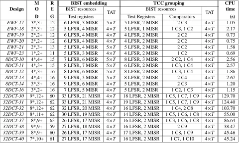
SUN SPARC 20 workstation using 6000 lines of C++ code. To give insight into the efficiency
of testability achieved using the presented approach Table 1 shows a comparison of BIST
re-sources and test application time (TAT) using the BIST embedding methodology and the TCC
grouping methodology. The results for the BIST embedding methodology were obtained
us-ing the same BIST hardware synthesis algorithm assumus-ing that every pair of modules in the
data path are different
nres nmod
as described in section 2.2. The comparison is carried out
for a number of benchmark examples including elliptic wave digital filter (EWF) and 8 and 32
point discrete cosine transform (DCT). The benchmarks were synthesized using the ARGEN
high-level synthesis system [35, 36] for different execution time constraints ranging from 10 to
40. For example, in the case of EWF-17 we have 6 modules (MOD), 3 multipliers (*) and 3
adders (+), and 12 registers (REG). The test application time lengths of adders and multipliers
are assumed to be T
T , and respectively T 4
T , where T is a reasonably large integer
and can be estimated for the required fault coverage using the techniques from [37]. It should
be noted that the proposed BIST hardware synthesis algorithm for RTL data paths provides the
flexibility of specifying the test application time for the expected fault coverage of 100% for
each data path module. In the experimental results reported in this section it was considered
T 64, and hence T
64 and T 256, for achieving 100% fault coverage for each 8 bit
data path module which is comparable with the test length values reported in [19]. To
vali-date the assumption regarding test length, adder and multiplier modules have been synthesized
single fault propagation fault simulator [39] has shown that T 64 is valid for 8 bit data path
modules. In general the TCC grouping methodology produces less test registers than the BIST
embedding methodology. For example, in the case of EWF-20 the number of LFSRs is reduced
from 6 to 4, and the number of MISRs is reduced from 4 to 2. There is further reduction as
the design complexity increases. For example, in the case of 32DCT-33 the number of LFSRs
is reduced from 30 to 14, and the number of MISRs is reduced from 19 to 2. The reduction in
test registers in case of TCC grouping is achieved at the expense of comparators. In the case of
32DCT-33 there are one 5 input comparator (C5), one 6 input comparator (C6) and one 8 input
comparator (C8). However, the TCC grouping methodology requires reduced BIST area
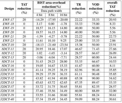
over-head when compared with the BIST embedding methodology as shown in Table 2 for data path
width varying from 4-bit up to 16-bit. Note that the proposed BIST methodology is capable
of dealing with variable bit width data paths as outlined in section 2.2. BIST area overhead is
computed using the equivalent number of 2 input gates required to modify functional registers
into LFSRs, MISRs and BILBOs, if applicable, and for implementing the comparators. For
benchmark circuit 32DCT-33 the reductions in BIST area overhead in terms of equivalent gates
are of 45.63% in the case of 4-bit data path, 43.72% in the case of 8-bit data path and 42.65% in
the case of 16-bit data path. But there are cases such as EWF-17 and 8DCT-13 where the BIST
embedding methodology produces better BIST area overheads. This has been achieved without
reaching the minimal TAT. For example circuits EWF-17 and 8DCT-13 reductions of 20% in
TAT are achieved by the TCC grouping methodology. This result is derived using the TAT from
Table 1, where the minimum reached TAT for the TCC grouping methodology is 5
T , and for
the BIST embedding methodology is 4
T .
So far the reductions in TAT and BIST area overhead achieved by the TCC grouping
method-ology when compared to the BIST embedding methodmethod-ology were outlined. Table 2 also shows
the reductions in number of test registers (TR), volume of output data (VOD), and overall test
application time (overall-TAT). The reduction in TR represents the reduction in the number of
data path registers modified in test registers and it may have direct impact on the performance
degradation (clock period). For example the reduction in TR for EWF-17 is 22.22%. The
re-duction in TR is increased up to 67.35% as in the case of 32DCT-33. Similarly the rere-duction
VOD varies from 33.33% in the case of EWF-17 up to 90.48% in the case of 32DCT-30 and
32DCT-31. The volume of output data is considered directly proportional to the number of
signature analysis registers. The number of signature analysis registers is very small due to the
large number of modules grouped in TCCs and reuse of signature analysis registers at
for test data but also on the overall test application time which consists of the test application
time (TAT) and the shifting time required to shift out the test responses at the end of the testing
process. The shifting time requires nSA
k clock cycles, where nSA is the number of signature
analysis registers and k is the data path width. The last column of Table 2 shows the reduction in
overall-TAT given the data path width as 8 bits and T 64. It should be noted that due to high
test concurrency, low test application time required for each data path module (T 64), and
high number of test registers, the value of shifting time is comparable to test application time.
This implies that the proposed BIST methodology leads to substantial savings in overall-TAT
due to the reduction in signature analysis registers. For all benchmark circuits where both BIST
embedding and TCC grouping methodologies achieved minimal test application time (4
T ) the
overall-TAT is reduced in the case of the TCC grouping methodology due to a smaller number
of signature analysis registers. For example, in the case 32DCT-30 the overall-TAT reduction
achieved by the TCC grouping methodology when compared to the BIST embedding
methodol-ogy is 35.85%. The BIST hardware synthesis algorithm has excellent computational time. The
CPU time required to achieve lowest TAT for benchmark circuits is shown in the last column
of Table 1. For example, in the case of EWF and 8 point DCT designs, the computational time
varies from 0.7s to 3s. In the case of designs with huge testable design space like 32 point DCT,
high quality solutions are achieved in computational times ranging from 38s to 130s. A high
quality solution is a fully testable data path with test application time equal (or almost equal) to
the longest test application time required to test the most random pattern resistant module (4
T
in the case of benchmark circuits of Table 1). It should be noted that despite the fact that test
registers and test schedule of the final solution are dependent on the initial random assignment
of test registers, the quality of the final solution (in terms of test application time and BIST
area overhead) is independent on the initial random assignment due to intelligent neighborhood
search outlined in section 3.
Although the emphasis of the work presented in this paper is on built-in self-testable data
paths the following discussion clarifies the issue of controlling the controller outputs while
test-ing the data path, and that of testtest-ing the controller itself. Since the proposed BIST methodology
targets data flow intensive applications there are only a few flip flops required to implement the
functional controller. For example, in the case of 32DCT-30 only 5 flip flops implement the
30 control states. Since control signals need to be controlled during testing, a BIST controller
is synthesized. However, the size of the BIST controller is small and the BIST controller can
easily be merged with the functional controller for both controlling the signals during data path
to the size of the data path. For example, in the case of 32DCT-30 the BIST controller consists
of 1 flip flop which indicates that data path is in test mode, 6 flip flops implementing the pattern
counter (T 2
6), 2 flip flops implementing test application controller (TAT=4
T ) and 1 flip
flop that switches between the phases of test application and shifting out test responses.
There-fore the entire controller (both functional and BIST controller) has only 15 flip flops which
is insignificant when compared to the size of data path (60 registers of which 18 LFSR and
2 MISR as shown in Table 1). The control signals controlling the data path are synthesized
using both functional and test specification and the control logic (which is insignificant when
compared to only one data path multiplier) is tested by configuring controller into a LFSR. This
does not add any performance degradation for data flow intensive applications since the clock
period is constrained by the critical path in the complex data path. Furthermore, both the size
of the merged controller and test application time of the controller is smaller in the case of the
proposed TCC grouping when compared to BIST embedding due to smaller number of cycles
required to shift out test responses and less logic required to implement control signals during
testing. If the random patterns generated by the LFSR are not satisfactory to detect all the faults
in the controller some additional DFT such as scan needs to be inserted. To provide the
com-plete test scenario, the work in [8, 9] lends itself well for the untested multiplexers and registers
since they necessitate only 4 test patterns regardless of the bit width. Therefore it is likely that
the size of the global set of functional patterns mentioned in section 2.1 will be small.
The BIST hardware synthesis for TCC grouping methodology allows the huge testable
de-sign space to be explored efficiently by combining the accuracy of incremental test scheduling
algorithms and the exploration speed of test scheduling algorithms based on fixed test resource
allocation, as outlined in section 3. This means it can be used with extremely complex
hypothet-ical designs of dimensions not often reported in literature. Complex hypothethypothet-ical data paths1
have been generated as described in the following. The number of modules nmod varies from
35 to 45, and the number of registers nregvaries from 90 to 115. The number of module-types
is nres 5. The maximum fanin for every register or input port of a module is Mf anin 8.
The input register set of each input port of every module contains a random number nr, with
1 nr Mf anin, of randomly chosen registers. Similarly, the number of modules multiplexed
at the input of each register is a random number nm, with 1 nm Mf anin, of randomly
cho-sen modules. The TAT of three module-types is assumed T , and in the case of the other two
module-types the TAT is considered 4
T . Figure 4 clearly demonstrates that the TCC grouping
methodology overcomes the problems of the BIST embedding in dealing with complex
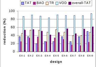
thetical data paths. The complex hypothetical data paths have been labelled EX 1 to EX 9.
For most of the designs the proposed TCC grouping reduces TAT when compared to BIST
embedding. However, when both BIST embedding and TCC grouping achieve low TAT, the
re-ductions in BIST area overhead, number of test registers (impact on performance degradation),
volume of output data and overall test application time are substantial. For example in the case
of EX-9 reductions of 50% in TAT, 23% in BAO, 47% in TR, 94% in VOD and 61% in overall
TAT are achieved. Furthermore, the computational time for obtaining high quality solutions is
still very low related to the size of the testable design space. For example it took less than 600s
to find high quality solutions for data paths with 45 modules and up to 115 registers.
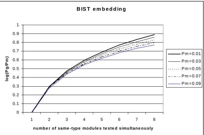
Finally, Figure 5 shows how the proposed TCC grouping methodology decreases the
fault-escape probability when compared to the BIST embedding methodology. The experiments
were done for a data path module with possible 106 error sequences, where the aliasing error
sequences, for a given characteristic polynomial of signature analysis register, vary from 10 to
90. Fault-escape probability of a module varies from Pm 001% to Pm 009%. As it can be
seen from Figure 5(a), in the case of BIST embedding methodology the fault escape probability
for group of modules
Pg increases as the number of modules tested simultaneously increases.
On the other hand, in the case of the TCC grouping, the fault-escape probability decreases
exponentially with the number of modules tested simultaneously as shown in Figure 5(b). This
is due to the fact that a fault is not detected in the TCC grouping methodology only when
initially the n-input k-bit comparator fails to detect the fault and subsequently the signature of
a TCC also fails to detect the fault. A previous work on reducing fault-escape probability at the
expense of increased area overhead, performance degradation, and volume of output data was
presented in [40]. Note that the proposed methodology does not introduce any area overhead,
nor performance degradation, whilst the reduction in fault-escape probability is exponential.
5
Conclusion
This paper has addressed the testability of RTL data paths. It has been shown that an
improve-ment in terms of test application time, BIST area overhead, performance degradation, volume
of output data, overall test application time (the sum of test application time and shifting time
required to shift out test responses) and fault-escape probability is achieved using the newly
introduced test compatibility classes-based methodology. The new BIST methodology is based
on grouping modules with identical physical information into TCCs and testing the compatible
k-bit comparator checks module output responses from each TCC reducing the fault-escape
probability
and the number of signatures that have to be shifted out. The proposed TCC
group-ing methodology is suitable for RTL data paths with both uniform and variable bit width. A
new BIST hardware synthesis uses efficient tabu search-based testable design space exploration
which combines the accuracy of incremental test scheduling algorithms with the exploration
speed of test scheduling algorithms based on fixed test resource allocation. The huge size of the
testable design space is reduced by considering only the representative partially testable data
paths during the local neighborhood search. An incremental TCC scheduling algorithm further
shrinks the size of the testable design space by generating a fully testable data path using
simul-taneous test scheduling and signature analysis registers allocation. BIST hardware synthesis
algorithm for the proposed TCC grouping methodology has been tested exhaustively for
bench-mark and complex hypothetical data paths. When compared to the traditional BIST
embed-ding methodology, the TCC grouping methodology is capable of reducing the test application
time with comparable of even lower BIST area overhead and high reductions in performance
degradation, volume of output data, fault-escape probability and overall test application time.
Furthermore the proposed BIST hardware synthesis algorithm achieves high quality of the final
solution in low computational time.
The proposed methodology and the BIST hardware synthesis algorithm have been
success-fully integrated in high-level synthesis design flow [36] leading to lower design cycle by
consid-ering testability at higher levels of abstraction than the gate-level. This reinforces the conclusion
reached recently by other researchers [6–8] that testability of digital circuits is best explored and
optimized at the register transfer level. Since the proposed methodology targets RTL data paths
of data flow intensive designs future work will investigate integrated controller/data path testing
for both data flow and control flow intensive circuits.
Acknowledgement
The authors would like to thank Professor Melvin Breuer of University of Southern California
References
[1] G. de Micheli, Synthesis and Optimization of Digital Circuits. McGraw-Hill International
Editions, 1994.
[2] M.C. McFarland, A.C. Parker, and R. Camposano, “The high-level synthesis of digital
systems,” Proceedings of the IEEE, vol. 78, pp. 301–318, Feb 1990.
[3] V. Chickername, J. Lee, and J.K. Patel, “Addressing design for testability at the
architec-tural level,” IEEE Transactions CAD, vol. 13, pp. 920–934, Jul 1994.
[4] S. Narayanan and M.A. Breuer, “Reconfiguration techniques for a single scan chain,”
IEEE Transactions on CAD, vol. 14, pp. 750–765, Jun 1995.
[5] R. Gupta and M.A. Breuer, “Partial scan design of register-transfer level circuits,” Journal
of Electronic Testing: Theory and Applications (JETTA), vol. 7, pp. 25–46, Aug 1995.
[6] S. Dey and M. Potkonjak, “Nonscan design-for-testability techniques using RT-level
de-sign information,” IEEE Transcations on CAD, vol. 16, pp. 1488–1506, Dec 1997.
[7] I. Ghosh, A. Raghunathan, and N.K. Jha, “Design for hierarchical testability of RTL
cir-cuits obtained by behavioral synthesis,” IEEE Transcations on CAD, vol. 16, pp. 1001–
1014, Sep 1997.
[8] I. Ghosh, A. Raghunathan, and N.K. Jha, “A design for testability technique for RTL
circuits using control/data flow extraction,” IEEE Transcations on CAD, vol. 17, pp. 706–
723, Aug 1998.
[9] Y. Makris and A. Orailoglu, “RTL test justification and propagation analysis for
modu-lar designs,” Journal of Electronic Testing: Theory and Applications (JETTA), vol. 13,
pp. 105–120, Oct 1998.
[10] V.D. Agrawal, C.R. Kime, and K.K. Saluja, “A tutorial on built-in self test - part 2:
Appli-cations,” IEEE Design and Test of Computers, pp. 69–77, Jun 1993.
[11] S. Boubezari, E. Cerny, B. Kaminska, and B. Nadeau-Dostie, “Testability analysis and
test-point insertion in RTL VHDL specifications for scan-based BIST,” IEEE Transactions
on CAD, vol. 18, pp. 1327–1340, Sep 1999.
[12] D. Gizopoulos, A. Paschalis, and Y. Zorian, “An effective BIST scheme for datapaths,” in
[13] D. Berthelot, M.L. Flottes, and B. Rouzeyre, “BISTing datapaths under heterogenous
test schemes,” Journal of Electronic Testing: Theory and Application (JETTA), vol. 14,
pp. 115–123, Jan 1999.
[14] I. Ghosh, N.K. Jha, and S. Bhawmik, “A BIST scheme for RTL circuits based on symbolic
testability analysis,” IEEE Transcations on CAD, vol. 19, pp. 111–128, Jan 2000.
[15] S. Ravi, N.K. Jha, and G. Lakshminarayana, “TAO-BIST: A framework for testability
analysis and optimization for built-in self-test of RTL circuits,” IEEE Transactions on
CAD, vol. 19, Aug 2000.
[16] L. Goodby and A. Orailoglu, “Redundancy and testability in digital filter datapaths,” IEEE
Transcations on CAD, vol. 18, pp. 631–644, May 1999.
[17] P.R. Chalsani, S. Bhawmik, A. Acharya, and P. Palchaudhuri, “Design of testable
VLSI circuits with minimum area overhead,” IEEE Transactions on Computers, vol. 38,
pp. 1460–1462, Sep 1989.
[18] A. Basu, T.C. Wilson, D.K. Banerji, and J.C. Majithia, “An approach to minimize
testa-bility for BILBO based built-in self-test,” in Proc. 5th International Conference on VLSI
Design, pp. 354–355, 1992.
[19] S.P. Lin, C.A. Njinda, and M.A. Breuer, “Generating a family of testable designs using the
BILBO methodology,” Journal of Electronic Testing: Theory and Applications (JETTA),
vol. 4, no. 2, pp. 71–89, 1994.
[20] G.L. Craig, C.R. Kime, and K.K. Saluja, “Test scheduling and control for VLSI built-in
self-test,” IEEE Transactions on Computers, vol. 37, pp. 1099–1109, Sep 1988.
[21] W.B. Jone, C.A. Papachristou, and M. Pereira, “A scheme for overlaying concurrent
test-ing of VLSI circuits,” in Proc. 26th Design Automation Conference, pp. 531–536, 1989.
[22] C.I.H. Chen, “Graph partitioning for concurrent test scheduling in VLSI circuits,” in Proc.
28th Design Automation Conference, pp. 287–290, 1991.
[23] H.B. Kim, T. Takahashi, and D.S. Ha, “Test session oriented built-in self-testable data path
synthesis,” in IEEE International Test Conference, pp. 154–163, 1998.
[24] A. Orailoglu and I.G. Harris, “Test path generation and test scheduling for self-testable
[25] I.G. Harris and A. Orailoglu, “Microarchitectural synthesis of VLSI designs with high test
concurrency,” in Proc. 31st Design Automation Conference, pp. 206–211, 1994.
[26] S. Chiu and C.A. Papachristou, “A desing for testability scheme with applications to data
path synthesis,” in Proc. 28th IEEE/ACM Design Automation Conference, pp. 271–277,
1991.
[27] E.J. McCluskey, “Design for testability,” in Logic Design Principles With Emphasis On
Testable Semicustom Circuits, pp. 424–488, New Jersey: Prentice Hall, 1986.
[28] S.K. Gupta and D.K. Pradhan, “Utilization of on-line (concurrent) checkers during built-in
self-test and vice versa,” IEEE Transactions on Computers, vol. 45, pp. 63–73, Jan 1996.
[29] M.F. Abdulla, C.P. Ravikumar, and A. Kumar, “Optimization of mutual and signature
testing schemes for highly concurrent systems,” Journal of Electronic Testing: Theory
and Applications (JETTA), vol. 12, pp. 199–216, June 1998.
[30] P.H. Bardell, W.H. McAnney, and J. Savir, Built-In Self Test - Pseudorandom Techniques.
John Wiley & Sons, 1986.
[31] D.G. Chinnery and K. Keutzer, “Closing the gap between ASIC and custom: An ASIC
per-spective,” in Proc. 37th IEEE/ACM Design Automation Conference, pp. 637–642, 2000.
[32] W.J. Dally and A. Chang, “The role of custom design in ASIC chips,” in Proc. 37th
IEEE/ACM Design Automation Conference, pp. 643–647, 2000.
[33] F. Glover and M. Laguna, “Tabu search,” in Modern Heuristic Techniques for
Combinato-rial Problems (C.R. Reeves, ed.), pp. 70–150, McGraw-Hill Book Company, 1995.
[34] N. Nicolici, “Power minimisation techniques for testing low power VLSI circuits,” Tech.
Rep. Upgrade from MPhil to PhD, University of Southampton, UK, December 1999.
[35] P. Kollig and B.M. Al-Hashimi, “A new approach to simultaneous scheduling, allocation
and binding in high level synthesis,” IEE Electronics Letters, vol. 33, pp. 1516–1518, Aug
1997.
[36] P. Kollig, Algorithms for Scheduling, Allocation and Binding in High Level Synthesis. PhD
thesis, Staffordshire University, UK, Apr 1998.
[37] A. Ma