Analysis of Self Checking Additional Adder
Circuit in Combinational Circuits
Abirami SB1, Manoj K2, Maruthupandian C3, Rajesh K4
1,2,3
Final year ECE, 4Assistant Professor ECE
1,2,3,4
Knowledge Institute Of Technology ,Salem ,India
Abstract— Digital computers perform variety of information tasks; among the functions encountered are the various arithmetic operations. The most basic arithmetic operation is the addition and subtraction of two or more binary digits. In processors adders are used not only in the arithmetic logic units, but also in other parts of the processor, where they are used to calculate addresses, table indices and similar operations. The basic building block of many complex computational systems is the full adder. VLSI integrates a large system into a single chip. Self checking scheme is becoming an important design technique to full fill the requirements of modern computer systems with full reliability. The main aim of this paper is to provide the output of ripple carry adder without any error even when any one of the full adder is fault. The proposed system is built using VHDL, simulated using Xilinx ISE 12.1 and implemented using Spartan-3E FPGA and ALTERA Universal kit. This will fit the specified functional requirements and finds a solution to overcome the problem of fault in any one full adder.
Keywords—Full adder, self-checking, modified adder, modified subtractor, combinational circuit, multiplexer.
I. INTRODUCTION
For any large combinational circuit there are generally two approaches to design. Taking simpler circuits and replicates them or designs the complex circuit as a complex device. Both the circuits allow spending less time to design and more time for signals to propagate through the transistors. So attempt to replace portions of the circuit that are too slow and faulty. It is possible to create a logical circuit using multiple full adders to add N-bit numbers. Each full adder inputs a Cin, which is the Cout of the previous adder. This kind of adder is called a ripple-carry adder, since each carry bit "ripples" to the next full adder. Note that the first (and only the first) full adder may be replaced by a half adder (under the assumption that Cin = 0).
The layout of a ripple-carry adder is simple, which allows for fast design time; however, the ripple-carry adder is relatively slow, since each full adder must wait for the carry bit to be calculated from the previous full adder. The gate delay can easily be calculated by inspection of the full adder circuit. Each full adder requires three levels of logic. In a 32-bit ripple-carry adder, there are 32 full adders, so the critical path (worst case) delay is 2 (from input to carry in first adder) + 31 * 3 (for carry propagation in later adders) = 95 gatedelays. The general equation for the worst-case delay for an n-bit carry-ripple adder is
S C HA
CRA
n
T
n
T
T
T
(
)
(
1
).
C
FA
n
T
T
(
1
).
D
n
Tc
n
D
(
1
).
(
2
).
2
6
--(1)The delay from bit position 0 to the carry-out is a little different:
D
n
D
T
n
T
T
CRA C HA Cout]
.
3
.
2
:0
[
-- (2)The carry-in must travel through n carry-generator blocks to have an effect on the carry-out
D
n
T
n
n
T
CRAC C C out](
)
..
.
2
:[ 0
-- (3)A design with alternating carry polarities and optimized AND-OR-Invert gates can be about twice as fast. To reduce the computation time, engineers devised faster ways to add two binary numbers by using carry-look ahead adders. They work by creating two signals (P and G) for each bit position, based on whether a carry is propagated through from a less significant bit position (at least one input is a '1'), generated in that bit position (both inputs are '1'), or killed in that bit position (both inputs are '0'). In most cases, P is simply the sum output of a half adder and G is the carry output of the same adder. After P and G are generated the carries for every bit position are created. Some advanced carry-look ahead architectures are the Manchester carry chain, Brent–Kung adder, and the Kogge–Stone adder. For all the adder circuit the combination of half adder and full adder has been used.
carry-Technology (IJRASET)
769
bypass) adder which will determine P and G values for each block rather than each bit, and the carry select adder which pre-generates the sum and carry values for either possible carry input (0 or 1) to the block, using multiplexers to select the appropriate result when the carry bit is known.Other adder designs include the carry-select adder, conditional sum adder, carry-skip adder, and carry-complete adder.
II. EXISTINGSYSTEM
A. One Bit Full Adder
A one-bit full adder is a combinational circuit that performs the arithmetic sum of three bits. It consists of three inputs a, b and cin and two outputs S and Cout [3] as illustrated in Fig. 1.Expressions for S and Cout are given in (1) and (2)
Fig1.A full adder block
S = a b cin--(1) Cout=a.b+b.cin+cin .a-- (2)
B. Full Subtractor
A one-bit full subtractor is a combinational circuit that performs subtraction of three bits. It has three inputs are X, Y and Z and the two outputs are D (difference) and B (borrow) as illustrated in Fig.2. Expressions for D and B are given in (1) and (2)
Fig 2.A full subtractor block
C. Multiplexer
A multiplexer (or mux) is a device that selects one of several analog or digital input signals and forwards the selected input into a single line. A multiplexer of 2n inputs has n select lines, which are used to select which input line to send to the output. Multiplexers are mainly used to increase the amount of data that can be sent over the network within a certain amount of time and bandwidth. A multiplexer is also called a data selector.
D. Four Bit Ripple Carry Adder
A simple ripple carry adder (RCA) is a digital circuit that produces the arithmetic sum of two binary numbers. It can be constructed with full adders connected in cascade, with the carry output from each full adder connected to the carry input of the next full adder in the chain. Fig. 2 shows the interconnection of four full adder (FA) circuits to provide a four bit ripple carry adder.
Fig4. A Four bit ripple carry adder
Notice from Fig. 2 that the input is from the right side because the first cell traditionally represents the least significant bit (LSB). Bits a0 and b0 in the figure represent the least significant bits of the numbers to be added. The sum output is represented by the bits S0 – S3. The main problem with this type of adder is the delays needed to produce the carry out signal and the most significant bit. These delays increase with the increase in the number of bits to be added.
E. Four Bit Ripple Borrow Subtractor
A ripple-borrow subtract or can be composed of a cascade of full subtractor. Two binary numbers A and B are subtracted from right to left, creating a difference and a borrow at the outputs of each full subtract or for each bit position. Fig. 5 shows the interconnection of four full subtractor (FS) circuits to provide a four bit ripple borrow subtractor.
Fig5.A Four bit ripple borrow subtractor
III. PROPOSEDSYSTEM
The proposed system provides the modified structure of the four bit ripple carry adder, four bit borrow subtractor and four bit 2’s complement borrow subtractor. The working principle and operation of the proposed system is similar as it before expect the number of adder and multiplexer increases in both the adder and subtractor. These is because the fault any full adder/subtractor is replaced with another adder /subtractor circuit. With this we can able to rectify the fault easily
Technology (IJRASET)
[image:5.612.199.414.87.248.2] [image:5.612.197.414.292.412.2]771
Fig 7.A Modified Four bit ripple borrow subtractorFig 8.A Modified Four bit ripple borrow subtractor (2’s complement)
IV. SIMULATIONRESULTSANDPERFORMANCECOMPARISON
[image:5.612.186.431.537.639.2]Even though the number of adder and mux in the modified binary adder and Subtractor architecture increases, any fault in one of the full adder can be replaced with another adder circuit. With this modified structure, we can able to rectify the fault easily. Fig shows the simulation result for 4-bit ripple carry adder done with the help of Xilinx12.1 and implemented in Spartan 3E FPGA board.
Fig 9.simulation of 4-bit ripple carry adder
Fig 10.Timing details of 4-bit ripple carry adder
Fig shows the simulation result for 4-bit ripple borrow subtractor done with the help of Xilinx12.1 and implemented in Spartan 3E FPGA board.
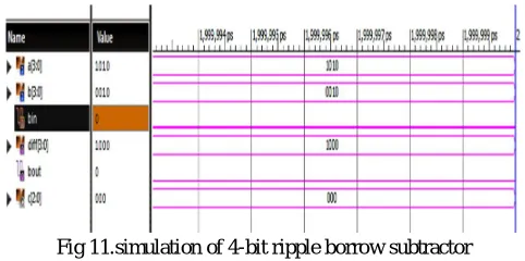
[image:6.612.193.421.554.692.2]Fig 11.simulation of 4-bit ripple borrow subtractor
Fig shows the timing details for 4 bit ripple borrow subtractor done with the help of Xilinx12.1.
Fig 12.Timing details of 4-bit ripple carry adder
Fig shows the simulation result for modified 4-bit ripple carry adder done with the help of Xilinx12.1 and implemented in Spartan 3E FPGA board.
Technology (IJRASET)
[image:7.612.189.426.83.232.2] [image:7.612.186.423.284.390.2] [image:7.612.187.427.419.522.2]773
Fig shows the timing details for modified 4 bit ripple carry adder done with the help of Xilinx12.1. [image:7.612.188.426.580.694.2]Fig 14.Timing details of modified 4-bit ripple carry adder
Fig shows the simulation result for 4 bit ripple borrow subtractor done with the help of Xilinx12.1 and implemented in Spartan 3E FPGA board.
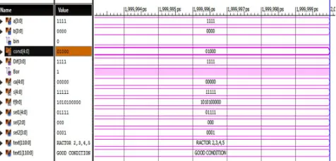
Fig 15.simulation of modified 4-bit ripple borrow subtractor
Fig shows the timing details for modified 4 bit ripple borrow subtractor done with the help of Xilinx12.1.
Fig 16.Timing details of modified 4-bit ripple borrow subtractor
Fig shows the simulation result for modified 4-bit ripple borrow subtractor 2’s complement done with the help of Xilinx12.1 and implemented in Spartan 3E FPGA board.
Fig shows the timing details for modified 4 bit ripple borrow subtractor 2’s complement done with the help of Xilinx12.1.
Fig 18.Timing details of modified 4-bit ripple borrow subtractor
TABLE1. COMPARISON OF ADDER AND SUBTRACTOR
Adder /
Subtractor Delay
Auto Correction
4 bit adder 8.959ns No
4 bit
Subtractor 9.208ns No
Modified 4
bit adder 8.304ns Yes
Modified 4 bit Subtractor
8.328ns Yes
V. CONCLUSION
The proposed full adder/subtractor system has been simulated and results are compared with existing full adder/subtractor system in terms of performance and delay. This proposed adder/subtractor system is having improvement in both of these aspects. The system is designed in auto correction format which is done with the help of extra one full adder/subtractor and multiplexer.
VI.ACKNOWLEDGMENT
We would like to thanks to the professor and Head of Department, Mrs.Dr.N.Santhiyakumari, Knowledge institute of technology, Salem and to the assistant Professor Mr.K.Rajesh, Kiot, Salem for his valuable help andguidance.
REFERENCES
[1] Z. Deng and A. M. Niknejad. (2010). The Speed-Power Trade-off in the Design of CMOS True-Single-Phase-Clock Dividers. IEEE Journal of Solid-State Circuits, Vol. 45, no. 11, pp. 2457–2465.
[2] J. N. Soares, JR and W. A. M. Van Noije. (1999). A 1.6-Ghz Dual Modulus Prescaler using the Extended True-Single Phase Clock CMOS Circuit Technique (E-TSPC). IEEE Journal of Solid-state circuits, Vol. 34, no. 1, pp.97–102.
[3] A. Keshavarzi, K. Roy, and C. F. Hawkins. (1997). Intrinsic Leakage in Low Power Deep Submicron CMOS ICs. In Proc. International Test Conference, pp. 146– 155.
[4] S.M. Kang, Y. Leblebici (2003). CMOS Digital Integrated Circuits Analysis and Design. Third Edition:Tata McGraw Hill.
[5] M. V. Krishna, M. A. Do, K. S. Yeo, C. Boon, and W. M. Lim (2010). Design and Analysis of Ultra Low Power True Single Phase Clock CMOS 2/3 Prescaler. IEEE Transactions: Circuits System. I, Reg. Papers, vol. 57, No. 1,pp. 72–82.
[6] H. J. M. Veendrick (1984).Short-Circuit Dissipation of Static CMOS Circuitry and its Impact on the Design of Buffer Circuits. IEEE Journal of Solid-State Circuits,Vol. SC-19, No. 4.
[7] X.-P. Yu, M. A. Do, W. M. Lim, K. S. Yeo, and J. G. Ma (2006). Design and Optimization of the Extended True Single-Phase Clock-Based Prescaler. IEEE Transactions: Microwave Theory Techniques, Vol. 54, no. 11, pp. 3828–3S835.
Technology (IJRASET)
©IJRASET 2015: All Rights are Reserved
775
[9] H. T. Bui, Y. Wang, and Y. Jiang, “Design and analysis of low-power 10-transistor full adders using XOR-XNOR gates,” IEEE Transactions CircuitsSystems II, Analog Digital Signal Process, vol. 49, no. 1, pp. 25– 30, Jan. 2002.
[10] S. Goel. A. Kumar, M. A. Bayoumi, “Design of robust, energy – efficient full adders for deep sub micrometer design using hybrid-CMOS logic style” IEEE Transactions on Very Large Scale Integration (VLSI) Systems, vol.14, no.12, pp.1309-1321, Dec. 2006.
[11] C Senthilpari, “A Low-power and High-performance Radix-4Multiplier Design Using a Modified Pass-transistor Logic Technique” IETE Journal of Research, Vol: 57, Issue No.: 2, Page: 149-155, May 2011.
[12] C.ChanneGowda Low-Power 1-Bit Full-Adder Cell Using Modified Pass Transistor Logicet al, / (IJCSIT) International Journal of Computer Science and Information Technologies, Vol. 4 (3) , 2013, 489-49.
[13] PallaviSaxena, UrvashiPurohit, Priyanka Joshi. Analysis of Low Power, Area- Efficient and High Speed Fast Adder. International Journal of Advanced Research in Computer and Communication Engineering Vol. 2, Issue 9, September 2013.