Three Phase Inverter Simulation using
Sinusoidal PWM Technique
Anubha Gupta
UG Student, Dept. of EE, PEC University of Technology, Chandigarh, India
ABSTRACT: This paper presents the simulation of three phase voltage switching inverter in MATLAB/Simulink using Sinusoidal Pulse Width Modulation (SPWM) scheme. The carrier wave (triangular) is compared to the reference (sine wave), whose frequency is the desired frequency. The modulation index is varied from 0.4 to 1 by changing the amplitude of the modulating signal. The output phase and line voltages are observed in scope along with their Total Harmonic Distortion (THD) which varies with modulation index. In SPWM technique, the amplitude is constant but the width of the pulse varies by changing the duty cycle for each period. The width of the pulses are modulated to provide gate signals to the switches (IGBTs) connected in the inverter. In this way the output voltage is controlled and THD also reduces significantly with the increase in efficiency of the inverter. This method is popularly used in speed control of three phase induction motors. The load taken here is resistive and inductive (RL).
KEYWORDS:Three phase inverter, MATLAB, Sinusoidal Pulse Width Modulation ,Modulation index.
I.INTRODUCTION
In today’s world most of the appliances and machines work on AC power. In the absence of AC power, there should be some way to convert DC power to AC power. This conversion is done by the power electronic circuit called the Inverter. The basic function of a power inverter is to change DC input voltage to a symmetric AC output voltage of the desired magnitude and frequency. These devices find wide applications in Uninterruptable Power Supplies (UPS), adjustable speed AC drives, induction heating and standby aircraft power supplies. If the DC input voltage is fixed but not controllable, a variable output voltage is obtained by varying the gain of the converter which is achieved by Pulse Width Modulation technique (PWM) control. The gain of the inverter is defined as the ratio of AC output voltage to that of DC input voltage.
There are two types of inverters-Voltage source and current source inverters. When an inverter has DC source with negligible resistance (which means that it has a stiff DC voltage source at its input terminals), it is said to be a voltage fed inverter or VSI. Whereas when it has a high input resistance (means it has a stiff DC current source at its input terminals), it is termed as current fed inverter or CSI.
II.PULSE WIDTH MODULATION (PWM)
In Pulse Width Modulation (PWM) technique, pulses of constant amplitude but different duty cycles are generated by modulating the time periods . This modulation is done by using one carrier and one reference signal . These two signals are fed to a comparator and the corresponding signals are generated based on the logic of the comparator. The reference wave is the desired signal output which may be a sine wave or a square wave. The carrier wave , on the other hand , is generally sawtooth or triangular wave having frequency significantly higher than that of the reference signal. The higher order harmonics in the load current are eliminated using a series inductor. A selected range of lower harmonics can be reduced by suitably choosing the number of pulses per half cycle.
Advantages of using PWM technique-
1. The output voltage can be controlled without using any additional component. 2. Significant reduction of lower order harmonics.
There are three basic PWM techniques- 1. Single pulse
3. Sinusoidal
In this paper only Sinusoidal PWM technique is implemented.
III.SINUSOIDAL PULSE WIDTH MODULATION (SPWM)
In Sinusoidal PWM, the width of each pulse is varied in proportion to the amplitude of the sine wave evaluated at the centre of the same pulse. The gating signals are generated by comparing a sinusoidal reference wave with a triangular carrier wave of frequency Fr and Fc respectively as shown in Figure 1. Fr determines the inverter output frequency foand
its peak amplitude Ar controls the Modulation Ratio (Ar/Ac) and hence the rms output voltage Vo. Several pulses per
half cycle are used and the pulse width is a sinusoidal function of angular position of pulses in a cycle. A high frequency carrier wave Vc is compared to a reference signal Vr having the desired frequency through a comparator.
When the sinusoidal wave has a higher magnitude, output is high otherwise it is low. The comparator output is processed in a trigger pulse generator in such a way that the output voltage wave has a pulse width in agreement with comparator pulse width.
Fig 1. Sinusoidal PWM
IV.SWITCHING TECHNIQUES
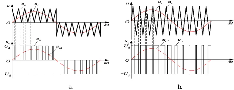
To provide the gate signals to the switches in an inverter, two types of switching schemes are used-Unipolar and Bipolar voltage switching. If the triangular carrier wave is either in the positive or negative polarity range of changes, the resulting SPWM wave lies only in the polarRange, this type of switching is called unipolar control mode. Whereas if the triangular carrier wave lies in continuous range between both positive and negative polarity, the SPWM wave lies between positive and negative changes, this switching is known as bipolar control. This is shown is Figure 2.
a. b.
V.THREE PHASE INVERTERS
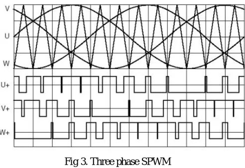
The three phase inverter is used to provide variable frequency power for industrial applications. SPWM is used for the voltage control of three phase inverters and the corresponding gating signals are shown in Figure 3. Here, triangular carrier wave is compared with three reference sinusoidal waves (U,V,W) which are displaced by 120 degrees.
Fig 3. Three phase SPWM
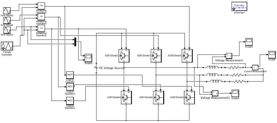
The basic circuit diagram of a three phase inverter with 6 IGBTs is shown in Figure 4.
Fig 4. Three phase inverter
The inverter is fed by a fixed dc voltage Vdc and has three phase-legs each comprising two IGBTs. With SPWM
The output voltage (line and phase) is measured across the Y connected RL load. The matlab/Simulink model is shown in Figure 5. The DC input voltage is kept as 400 V. The load resistor and inductor values are chosen to be 2 ohm and 6.5 mH.
Fig 5. Matlab/Simulink model
The gate pulses given to the three phase inverter are shown in Figure 6. The frequency of the carrier wave is kept 1000 Hz whereas for reference sine wave, it is 50 Hz.
Fig 6. a) Gate pulses for T1
Discrete,
Ts=5e-05s.
powergui v + -VoltageMeasurement Sine Wave1 +
DCVoltageSource1
Scope Scope1 Triangle Generator + + i + -Current Measurement Sine Wave3 Sine Wave4 >= Relational Operator2 >= Relational Operator5 >= Relational Operator7 Scope2 v +
Fig 6. b) Gate pulses for T3
Fig 6. c) Gate pulses for T5
VI.RESULTS
The resultant phase and line voltages are shown in Figure 7.
Fig 7. a) Phase voltage
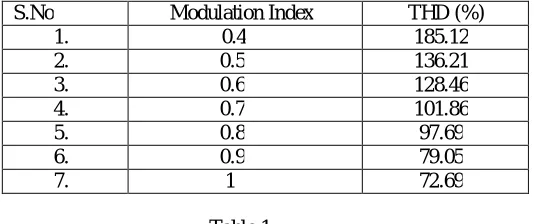
The FFT analysis is done to calculate Total Harmonic Distortion (THD) by varying the modulation index from 0.4 to 1. The results are tabulated below in Table 1.
S.No Modulation Index THD (%)
1. 0.4 185.12
2. 0.5 136.21
3. 0.6 128.46
4. 0.7 101.86
5. 0.8 97.69
6. 0.9 79.05
7. 1 72.69
Table 1
VII.CONCLUSION
The simulation of three phase inverters is carried out in MATLAB/Simulink where a simple control strategy i.e. Sinusoidal Pulse Width Modulation is applied for switching the switches. The total harmonic distortion for different modulation index is calculated and compared for RL load. As it can be seen from the results that as the modulation index approaches one, THD reduces significantly. SPWM technique is a common method used to provide gate signals to the switches in three phase inverter circuit.
REFERENCES
[1] Bhimbra P.S., “PowerElectronics” ,KhannaPublishers,Fourth Edition.
[2] Mohan, N., Undeland, T.M., Robbins, W.P., 1995. “Power Electronics, Converters, Applications and Design”, Second Edition, John Wiley &
Sons, Singapore.
[3] Muhammad H. Rashid, “Power electronics: circuits, devices, and applications”, Third Edition. 2004, Pearson/Prentice Hall.
[4] Maheshri S, KhampariyaP , “Simulation of single phase SPWM inverter,” IJIRAE Mag., vol. 1,isuuue 9, Oct. 2014.
[5] Dutta A, “Some aspects on three phase bridge inverter” , IJEI , vol 3, issue 4,pp:18-21,Nov 2013
[6] Mathukiya M.G., “three phase inverter with 180 and 120 conduction mode”, IJMTER ,vol. 4,issue 3,pp. 113–118 ,Mar 2017.
[7] Pankaj H Zope, PravinG.Bhangale, PrashantSonare ,S. R.Suralkar “Design and Implementation of carrier based SPWM Inverter”,