IA-32 Intel
®
Architecture
Software Developer’s
Manual
Volume 2A:
Instruction Set Reference, A-M
INFORMATION IN THIS DOCUMENT IS PROVIDED IN CONNECTION WITH INTEL PRODUCTS. NO LICENSE, EXPRESS OR IMPLIED, BY ESTOPPEL OR OTHERWISE, TO ANY INTELLECTUAL PROPERTY RIGHTS IS GRANTED BY THIS DOCUMENT. EXCEPT AS PROVIDED IN INTEL’S TERMS AND CONDITIONS OF SALE FOR SUCH PRODUCTS, INTEL ASSUMES NO LIABILITY WHATSOEVER, AND INTEL DISCLAIMS ANY EXPRESS OR IMPLIED WARRANTY, RELATING TO SALE AND/OR USE OF INTEL PRODUCTS INCLUDING LIABILITY OR WARRANTIES RELATING TO FITNESS FOR A PARTICULAR PURPOSE, MERCHANTABILITY, OR INFRINGEMENT OF ANY PATENT, COPYRIGHT OR OTHER INTELLECTUAL PROPERTY RIGHT. INTEL PRODUCTS ARE NOT INTENDED FOR USE IN MEDICAL, LIFE SAVING, OR LIFE SUSTAINING APPLICATIONS.
Intel may make changes to specifications and product descriptions at any time, without notice.
Developers must not rely on the absence or characteristics of any features or instructions marked "reserved" or "undefined." Improper use of reserved or undefined features or instructions may cause unpredictable behavior or failure in developer's software code when running on an Intel processor. Intel reserves these features or instructions for future definition and shall have no responsibility whatsoever for conflicts or incompatibilities arising from their unauthorized use.
The Intel® IA-32 architecture processors (e.g., Pentium® 4 and Pentium III processors) may contain design defects or errors known as errata. Current characterized errata are available on request.
Threading Technology requires a computer system with an Intel® Pentium® 4 processor supporting Hyper-Threading Technology and an HT Technology enabled chipset, BIOS and operating system. Performance will vary depending on the specific hardware and software you use. See http://www.intel.com/info/hyperthreading/ for more information including details on which processors support HT Technology.
Intel, Intel386, Intel486, Pentium, Intel Xeon, Intel NetBurst, Intel SpeedStep, OverDrive, MMX, Celeron, and Itanium are trademarks or registered trademarks of Intel Corporation and its subsidiaries in the United States and other countries.
*Other names and brands may be claimed as the property of others.
Contact your local Intel sales office or your distributor to obtain the latest specifications and before placing your product order.
Copies of documents which have an ordering number and are referenced in this document, or other Intel literature, may be obtained from:
Intel Corporation P.O. Box 5937 Denver, CO 80217-9808 or call 1-800-548-4725
or visit Intel’s website at http://www.intel.com
CONTENTS FOR VOLUME 2A AND 2B
PAGE
CHAPTER 1
ABOUT THIS MANUAL
1.1 IA-32 PROCESSORS COVERED IN THIS MANUAL . . . 1-1 1.2 OVERVIEW OF VOLUME 2A AND 2B: INSTRUCTION SET REFERENCE. . . 1-2 1.3 NOTATIONAL CONVENTIONS . . . 1-2 1.3.1 Bit and Byte Order . . . .1-2 1.3.2 Reserved Bits and Software Compatibility . . . .1-3 1.3.3 Instruction Operands . . . .1-4 1.3.4 Hexadecimal and Binary Numbers . . . .1-4 1.3.5 Segmented Addressing . . . .1-4 1.3.6 Exceptions . . . .1-5 1.3.7 A New Syntax for CPUID, CR, and MSR Values . . . .1-5 1.4 RELATED LITERATURE . . . 1-7
CHAPTER 2
INSTRUCTION FORMAT
2.1 INSTRUCTION FORMAT FOR PROTECTED MODE, REAL-ADDRESS
MODE, AND VIRTUAL-8086 MODE . . . 2-1 2.1.1 Instruction Prefixes . . . .2-2 2.1.2 Opcodes . . . .2-3 2.1.3 ModR/M and SIB Bytes . . . .2-4 2.1.4 Displacement and Immediate Bytes . . . .2-4 2.1.5 Addressing-Mode Encoding of ModR/M and SIB Bytes . . . .2-5 2.2 IA-32E MODE. . . 2-9 2.2.1 REX Prefixes . . . .2-9 2.2.1.1 Encoding. . . 2-10 2.2.1.2 More on REX Prefix Fields . . . 2-10 2.2.1.3 Displacement . . . 2-13 2.2.1.4 Direct Memory-Offset MOVs. . . 2-14 2.2.1.5 Immediates . . . 2-14 2.2.1.6 RIP-Relative Addressing. . . 2-14 2.2.1.7 Default 64-Bit Operand Size . . . 2-15 2.2.2 Additional Encodings for Control and Debug Registers . . . .2-15
CHAPTER 3
INSTRUCTION SET REFERENCE, A-M
CONTENTS
iv Vol. 2A
PAGE
3.1.1.11 Protected Mode Exceptions Section. . . 3-14 3.1.1.12 Real-Address Mode Exceptions Section . . . 3-15 3.1.1.13 Virtual-8086 Mode Exceptions Section. . . 3-15 3.1.1.14 Floating-Point Exceptions Section . . . .3-15 3.1.1.15 SIMD Floating-Point Exceptions Section . . . 3-16 3.1.1.16 Compatibility Mode Exceptions Section . . . 3-16 3.1.1.17 64-Bit Mode Exceptions Section. . . 3-16 3.2 INSTRUCTIONS (A-M) . . . 3-17 AAD—ASCII Adjust AX Before Division . . . 3-20 AAM—ASCII Adjust AX After Multiply . . . 3-22 AAS—ASCII Adjust AL After Subtraction . . . 3-24 ADC—Add with Carry . . . 3-26 ADD—Add . . . 3-29 ADDPD—Add Packed Double-Precision Floating-Point Values . . . 3-32 ADDPS—Add Packed Single-Precision Floating-Point Values . . . 3-35 ADDSD—Add Scalar Double-Precision Floating-Point Values . . . 3-38 ADDSS—Add Scalar Single-Precision Floating-Point Values. . . 3-41 ADDSUBPD: Packed Double-FP Add/Subtract. . . 3-44 ADDSUBPS: Packed Single-FP Add/Subtract . . . .3-48 AND—Logical AND . . . 3-52 ANDPD—Bitwise Logical AND of Packed Double-Precision
Floating-Point Values. . . 3-55 ANDPS—Bitwise Logical AND of Packed Single-Precision
Floating-Point Values. . . 3-57 ANDNPD—Bitwise Logical AND NOT of Packed Double-Precision
Floating-Point Values. . . 3-59 ANDNPS—Bitwise Logical AND NOT of Packed Single-Precision
Floating-Point Values. . . 3-61 ARPL—Adjust RPL Field of Segment Selector . . . 3-63 BOUND—Check Array Index Against Bounds . . . .3-65 BSF—Bit Scan Forward . . . 3-67 BSR—Bit Scan Reverse . . . 3-69 BSWAP—Byte Swap. . . 3-71 BT—Bit Test . . . 3-73 BTC—Bit Test and Complement . . . 3-76 BTR—Bit Test and Reset . . . 3-79 BTS—Bit Test and Set . . . 3-82 CALL—Call Procedure . . . 3-85 CBW/CWDE/CDQE—Convert Byte to Word/Convert Word to
CONTENTS
PAGE
CMPPD—Compare Packed Double-Precision Floating-Point Values . . . 3-121 CMPPS—Compare Packed Single-Precision Floating-Point Values. . . 3-126 CMPS/CMPSB/CMPSW/CMPSD/CMPSQ—Compare String Operands . . . . 3-131 CMPSD—Compare Scalar Double-Precision Floating-Point Values. . . 3-136 CMPSS—Compare Scalar Single-Precision Floating-Point Values . . . 3-140 CMPXCHG—Compare and Exchange . . . 3-144 CMPXCHG8B/CMPXCHG16B—Compare and Exchange Bytes . . . 3-147 COMISD—Compare Scalar Ordered Double-Precision Floating-Point
Values and Set EFLAGS . . . 3-150 COMISS—Compare Scalar Ordered Single-Precision Floating-Point
Values and Set EFLAGS . . . 3-153 CPUID—CPU Identification . . . 3-156 CVTDQ2PD—Convert Packed Doubleword Integers to Packed
Double-Precision Floating-Point Values. . . 3-179 CVTDQ2PS—Convert Packed Doubleword Integers to Packed
Single-Precision Floating-Point Values . . . 3-181 CVTPD2DQ—Convert Packed Double-Precision Floating-Point
Values to Packed Doubleword Integers . . . 3-184 CVTPD2PI—Convert Packed Double-Precision Floating-Point
Values to Packed Doubleword Integers . . . 3-187 CVTPD2PS—Convert Packed Double-Precision Floating-Point
Values to Packed Single-Precision Floating-Point Values . . . 3-190 CVTPI2PD—Convert Packed Doubleword Integers to Packed
Double-Precision Floating-Point Values. . . 3-193 CVTPI2PS—Convert Packed Doubleword Integers to Packed
Single-Precision Floating-Point Values . . . 3-196 CVTPS2DQ—Convert Packed Single-Precision Floating-Point
Values to Packed Doubleword Integers . . . 3-199 CVTPS2PD—Convert Packed Single-Precision Floating-Point
Values to Packed Double-Precision Floating-Point Values . . . 3-202 CVTPS2PI—Convert Packed Single-Precision Floating-Point
Values to Packed Doubleword Integers . . . 3-205 CVTSD2SI—Convert Scalar Double-Precision Floating-Point Value
to Doubleword Integer . . . 3-208 CVTSD2SS—Convert Scalar Double-Precision Floating-Point Value
to Scalar Single-Precision Floating-Point Value. . . 3-211 CVTSI2SD—Convert Doubleword Integer to Scalar Double-Precision
Floating-Point Value . . . 3-214 CVTSI2SS—Convert Doubleword Integer to Scalar Single-Precision
Floating-Point Value . . . 3-217 CVTSS2SD—Convert Scalar Single-Precision Floating-Point Value to
Scalar Double-Precision Floating-Point Value . . . 3-220 CVTSS2SI—Convert Scalar Single-Precision Floating-Point Value to
Doubleword Integer . . . 3-223 CVTTPD2PI—Convert with Truncation Packed Double-Precision
CONTENTS
vi Vol. 2A
PAGE
CVTTPD2DQ—Convert with Truncation Packed Double-Precision
Floating-Point Values to Packed Doubleword Integers . . . .3-229 CVTTPS2DQ—Convert with Truncation Packed Single-Precision
Floating-Point Values to Packed Doubleword Integers . . . .3-232 CVTTPS2PI—Convert with Truncation Packed Single-Precision
Floating-Point Values to Packed Doubleword Integers . . . .3-235 CVTTSD2SI—Convert with Truncation Scalar Double-Precision
Floating-Point Value to Signed Doubleword Integer . . . .3-238 CVTTSS2SI—Convert with Truncation Scalar Single-Precision
Floating-Point Value to Doubleword Integer . . . .3-241 CWD/CDQ/CQO—Convert Word to Doubleword/Convert Doubleword
to Quadword . . . .3-244 DAA—Decimal Adjust AL after Addition . . . .3-246 DAS—Decimal Adjust AL after Subtraction. . . .3-248 DEC—Decrement by 1 . . . .3-250 DIV—Unsigned Divide. . . .3-252 DIVPD—Divide Packed Double-Precision Floating-Point Values . . . .3-256 DIVPS—Divide Packed Single-Precision Floating-Point Values . . . .3-259 DIVSD—Divide Scalar Double-Precision Floating-Point Values . . . .3-262 DIVSS—Divide Scalar Single-Precision Floating-Point Values . . . .3-265 EMMS—Empty MMX Technology State . . . .3-268 ENTER—Make Stack Frame for Procedure Parameters . . . .3-270 F2XM1—Compute 2x–1 . . . .3-273 FABS—Absolute Value . . . .3-275 FADD/FADDP/FIADD—Add . . . .3-277 FBLD—Load Binary Coded Decimal . . . .3-281 FBSTP—Store BCD Integer and Pop . . . .3-283 FCHS—Change Sign . . . .3-286 FCLEX/FNCLEX—Clear Exceptions . . . .3-288 FCMOVcc—Floating-Point Conditional Move . . . .3-290 FCOMI/FCOMIP/ FUCOMI/FUCOMIP—Compare Floating Point Values
CONTENTS
PAGE
FMUL/FMULP/FIMUL—Multiply . . . 3-338 FNOP—No Operation . . . 3-342 FPATAN—Partial Arctangent. . . 3-343 FPREM—Partial Remainder . . . 3-346 FPREM1—Partial Remainder . . . 3-349 FPTAN—Partial Tangent . . . 3-352 FRNDINT—Round to Integer. . . 3-355 FRSTOR—Restore x87 FPU State . . . 3-357 FSAVE/FNSAVE—Store x87 FPU State . . . 3-360 FSCALE—Scale . . . 3-364 FSIN—Sine . . . 3-367 FSINCOS—Sine and Cosine . . . 3-369 FSQRT—Square Root . . . 3-372 FST/FSTP—Store Floating Point Value. . . 3-374 FSTCW/FNSTCW—Store x87 FPU Control Word . . . 3-377 FSTENV/FNSTENV—Store x87 FPU Environment. . . 3-380 FSTSW/FNSTSW—Store x87 FPU Status Word . . . 3-383 FSUB/FSUBP/FISUB—Subtract . . . 3-386 FSUBR/FSUBRP/FISUBR—Reverse Subtract . . . 3-390 FTST—TEST . . . 3-394 FUCOM/FUCOMP/FUCOMPP—Unordered Compare Floating Point
Values . . . 3-396 FXAM—ExamineModR/M . . . 3-399 FXCH—Exchange Register Contents . . . 3-401 FXRSTOR—Restore x87 FPU, MMX Technology, SSE, SSE2, and
CONTENTS
viii Vol. 2A
PAGE
LAR—Load Access Rights Byte . . . .3-504 LDDQU: Load Unaligned Integer 128 Bits. . . .3-508 LDMXCSR—Load MXCSR Register . . . .3-511 LDS/LES/LFS/LGS/LSS—Load Far Pointer . . . .3-514 LEA—Load Effective Address . . . .3-520 LEAVE—High Level Procedure Exit . . . .3-523 LFENCE—Load Fence . . . .3-525 LGDT/LIDT—Load Global/Interrupt Descriptor Table Register . . . .3-526 LLDT—Load Local Descriptor Table Register. . . .3-529 LMSW—Load Machine Status Word. . . .3-531 LOCK—Assert LOCK# Signal Prefix . . . .3-533 LODS/LODSB/LODSW/LODSD/LODSQ—Load String . . . .3-535 LOOP/LOOPcc—Loop According to ECX Counter . . . .3-538 LSL—Load Segment Limit. . . .3-541 LTR—Load Task Register . . . .3-545 MASKMOVDQU—Store Selected Bytes of Double Quadword . . . .3-547 MASKMOVQ—Store Selected Bytes of Quadword. . . .3-550 MAXPD—Return Maximum Packed Double-Precision
Floating-Point Values. . . .3-553 MAXPS—Return Maximum Packed Single-Precision
Floating-Point Values. . . .3-556 MAXSD—Return Maximum Scalar Double-Precision
Floating-Point Value. . . .3-559 MAXSS—Return Maximum Scalar Single-Precision
Floating-Point Value. . . .3-562 MFENCE—Memory Fence . . . .3-565 MINPD—Return Minimum Packed Double-Precision
Floating-Point Values. . . .3-566 MINPS—Return Minimum Packed Single-Precision
Floating-Point Values. . . .3-569 MINSD—Return Minimum Scalar Double-Precision
Floating-Point Value. . . .3-572 MINSS—Return Minimum Scalar Single-Precision Floating-Point
Value . . . .3-575 MONITOR: Setup Monitor Address . . . .3-578 MOV—Move . . . .3-581 MOV—Move to/from Control Registers . . . .3-587 MOV—Move to/from Debug Registers . . . .3-590 MOVAPD—Move Aligned Packed Double-Precision Floating-Point
Values . . . .3-592 MOVAPS—Move Aligned Packed Single-Precision Floating-Point
CONTENTS
PAGE
MOVDQ2Q—Move Quadword from XMM to MMX Technology
Register . . . 3-609 MOVHLPS— Move Packed Single-Precision Floating-Point Values
High to Low . . . 3-611 MOVHPD—Move High Packed Double-Precision Floating-Point Value . . . 3-613 MOVHPS—Move High Packed Single-Precision Floating-Point Values . . . 3-616 MOVLHPS—Move Packed Single-Precision Floating-Point Values
Low to High . . . 3-619 MOVLPD—Move Low Packed Double-Precision Floating-Point Value . . . 3-621 MOVLPS—Move Low Packed Single-Precision Floating-Point Values. . . 3-624 MOVMSKPD—Extract Packed Double-Precision Floating-Point
Sign Mask . . . 3-627 MOVMSKPS—Extract Packed Single-Precision Floating-Point
Sign Mask . . . 3-629 MOVNTDQ—Store Double Quadword Using Non-Temporal Hint. . . 3-631 MOVNTI—Store Doubleword Using Non-Temporal Hint . . . 3-634 MOVNTPD—Store Packed Double-Precision Floating-Point Values
Using Non-Temporal Hint. . . 3-636 MOVNTPS—Store Packed Single-Precision Floating-Point Values
Using Non-Temporal Hint. . . 3-639 MOVNTQ—Store of Quadword Using Non-Temporal Hint . . . 3-642 MOVSHDUP: Move Packed Single-FP High and Duplicate . . . 3-645 MOVSLDUP: Move Packed Single-FP Low and Duplicate . . . 3-648 MOVQ—Move Quadword . . . 3-651 MOVQ2DQ—Move Quadword from MMX Technology to XMM
Register . . . 3-654 MOVS/MOVSB/MOVSW/MOVSD/MOVSQ—Move Data from
String to String . . . 3-656 MOVSD—Move Scalar Double-Precision Floating-Point Value . . . 3-660 MOVSS—Move Scalar Single-Precision Floating-Point Values . . . 3-663 MOVSX/MOVSXD—Move with Sign-Extension . . . 3-666 MOVUPD—Move Unaligned Packed Double-Precision
Floating-Point Values . . . 3-668 MOVUPS—Move Unaligned Packed Single-Precision
Floating-Point Values . . . 3-670 MOVZX—Move with Zero-Extend . . . 3-673 MUL—Unsigned Multiply . . . 3-675 MULPD—Multiply Packed Double-Precision Floating-Point Values . . . 3-678 MULPS—Multiply Packed Single-Precision Floating-Point Values . . . 3-681 MULSD—Multiply Scalar Double-Precision Floating-Point Values . . . 3-684 MULSS—Multiply Scalar Single-Precision Floating-Point Values . . . 3-687 MWAIT: Monitor Wait. . . 3-690
CHAPTER 4
INSTRUCTION SET REFERENCE, N-Z
CONTENTS
x Vol. 2A
PAGE
OR—Logical Inclusive OR. . . .4-7 ORPD—Bitwise Logical OR of Double-Precision Floating-Point Values . . . 4-10 ORPS—Bitwise Logical OR of Single-Precision Floating-Point Values . . . 4-12 OUT—Output to Port . . . 4-14 OUTS/OUTSB/OUTSW/OUTSD—Output String to Port. . . 4-16 PACKSSWB/PACKSSDW—Pack with Signed Saturation . . . 4-21 PACKUSWB—Pack with Unsigned Saturation . . . 4-25 PADDB/PADDW/PADDD—Add Packed Integers . . . 4-29 PADDQ—Add Packed Quadword Integers . . . 4-33 PADDSB/PADDSW—Add Packed Signed Integers with Signed Saturation. . . .4-36 PADDUSB/PADDUSW—Add Packed Unsigned Integers with Unsigned
Saturation. . . 4-40 PAND—Logical AND . . . 4-44 PANDN—Logical AND NOT . . . .4-47 PAUSE—Spin Loop Hint . . . 4-50 PAVGB/PAVGW—Average Packed Integers . . . 4-51 PCMPEQB/PCMPEQW/PCMPEQD— Compare Packed Data for Equal . . . 4-54 PCMPGTB/PCMPGTW/PCMPGTD—Compare Packed Signed Integers
CONTENTS
PAGE
PSUBSB/PSUBSW—Subtract Packed Signed Integers with Signed
Saturation . . . 4-160 PSUBUSB/PSUBUSW—Subtract Packed Unsigned Integers with
Unsigned Saturation. . . 4-164 PUNPCKHBW/PUNPCKHWD/PUNPCKHDQ/PUNPCKHQDQ—
Unpack High Data . . . 4-168 PUNPCKLBW/PUNPCKLWD/PUNPCKLDQ/PUNPCKLQDQ—
Unpack Low Data . . . 4-173 PUSH—Push Word or Doubleword Onto the Stack . . . 4-178 PUSHA/PUSHAD—Push All General-Purpose Registers . . . 4-182 PUSHF/PUSHFD—Push EFLAGS Register onto the Stack . . . 4-184 PXOR—Logical Exclusive OR . . . 4-187 RCL/RCR/ROL/ROR-—Rotate . . . 4-190 RCPPS—Compute Reciprocals of Packed Single-Precision
Floating-Point Values . . . 4-196 RCPSS—Compute Reciprocal of Scalar Single-Precision
Floating-Point Values . . . 4-199 RDMSR—Read from Model Specific Register. . . 4-202 RDPMC—Read Performance-Monitoring Counters . . . 4-204 RDTSC—Read Time-Stamp Counter . . . 4-207 REP/REPE/REPZ/REPNE /REPNZ—Repeat String Operation Prefix . . . 4-209 RET—Return from Procedure . . . 4-214 RSM—Resume from System Management Mode. . . 4-225 RSQRTPS—Compute Reciprocals of Square Roots of Packed
Single-Precision Floating-Point Values . . . 4-227 RSQRTSS—Compute Reciprocal of Square Root of Scalar
Single-Precision Floating-Point Value . . . 4-230 SAHF—Store AH into Flags. . . 4-233 SAL/SAR/SHL/SHR—Shift . . . 4-235 SBB—Integer Subtraction with Borrow . . . 4-241 SCAS/SCASB/SCASW/SCASD—Scan String . . . 4-244 SETcc—Set Byte on Condition . . . 4-249 SFENCE—Store Fence . . . 4-253 SGDT—Store Global Descriptor Table Register . . . 4-254 SHLD—Double Precision Shift Left . . . 4-257 SHRD—Double Precision Shift Right . . . 4-260 SHUFPD—Shuffle Packed Double-Precision Floating-Point Values. . . 4-263 SHUFPS—Shuffle Packed Single-Precision Floating-Point Values . . . 4-266 SIDT—Store Interrupt Descriptor Table Register . . . 4-269 SLDT—Store Local Descriptor Table Register . . . 4-272 SMSW—Store Machine Status Word . . . 4-274 SQRTPS—Compute Square Roots of Packed Single-Precision
Floating-Point Values . . . 4-279 SQRTSD—Compute Square Root of Scalar Double-Precision
Floating-Point Value . . . 4-282 SQRTSS—Compute Square Root of Scalar Single-Precision
CONTENTS
xii Vol. 2A
PAGE
STC—Set Carry Flag. . . .4-288 STD—Set Direction Flag . . . .4-289 STI—Set Interrupt Flag . . . .4-290 STMXCSR—Store MXCSR Register State . . . .4-293 STOS/STOSB/STOSW/STOSD/STOSQ—Store String . . . .4-295 STR—Store Task Register . . . .4-299 SUB—Subtract . . . .4-301 SUBPD—Subtract Packed Double-Precision Floating-Point Values. . . .4-304 SUBPS—Subtract Packed Single-Precision Floating-Point Values . . . .4-307 SUBSD—Subtract Scalar Double-Precision Floating-Point Values . . . .4-310 SUBSS—Subtract Scalar Single-Precision Floating-Point Values . . . .4-313 SWAPGS—Swap GS Base Register . . . .4-316 SYSCALL—Fast System Call . . . .4-318 SYSENTER—Fast System Call . . . .4-320 SYSEXIT—Fast Return from Fast System Call. . . .4-324 SYSRET—Return From Fast System Call . . . .4-328 TEST—Logical Compare. . . .4-330 UCOMISD—Unordered Compare Scalar Double-Precision
Floating-Point Values and Set EFLAGS . . . .4-333 UCOMISS—Unordered Compare Scalar Single-Precision
Floating-Point Values and Set EFLAGS . . . .4-336 UD2—Undefined Instruction . . . .4-339 UNPCKHPD—Unpack and Interleave High Packed Double-Precision
Floating-Point Values. . . .4-340 UNPCKHPS—Unpack and Interleave High Packed Single-Precision
Floating-Point Values. . . .4-343 UNPCKLPD—Unpack and Interleave Low Packed Double-Precision
Floating-Point Values. . . .4-346 UNPCKLPS—Unpack and Interleave Low Packed Single-Precision
Floating-Point Values . . . .4-349 VERR/VERW—Verify a Segment for Reading or Writing . . . .4-352 WAIT/FWAIT—Wait. . . .4-355 WBINVD—Write Back and Invalidate Cache . . . .4-357 WRMSR—Write to Model Specific Register . . . .4-359 XADD—Exchange and Add. . . .4-361 XCHG—Exchange Register/Memory with Register . . . .4-363 XLAT/XLATB—Table Look-up Translation . . . .4-366 XOR—Logical Exclusive OR . . . .4-368 XORPD—Bitwise Logical XOR for Double-Precision
Floating-Point Values. . . .4-371 XORPS—Bitwise Logical XOR for Single-Precision
Floating-Point Values. . . .4-373
APPENDIX A OPCODE MAP
CONTENTS
PAGE
A.2.2 Codes for Operand Type . . . A-3 A.2.3 Register Codes . . . A-4 A.3 OPCODE LOOK-UP EXAMPLES . . . A-4 A.3.1 One-Byte Opcode Instructions. . . A-4 A.3.2 Two-Byte Opcode Instructions. . . A-5 A.3.3 Opcode Map Notes . . . A-6 A.3.4 Opcode Extensions for One-Byte and Two-Byte Opcodes . . . A-18 A.3.5 Escape Opcode Instructions . . . A-22 A.3.5.1 Escape Opcodes with D8 as First Byte. . . A-23 A.3.5.2 Escape Opcodes with D9 as First Byte. . . A-24 A.3.5.3 Escape Opcodes with DA as First Byte . . . A-25 A.3.5.4 Escape Opcodes with DB as First Byte . . . A-26 A.3.5.5 Escape Opcodes with DC as First Byte . . . A-27 A.3.5.6 Escape Opcodes with DD as First Byte . . . A-28 A.3.5.7 Escape Opcodes with DE as First Byte . . . A-29 A.3.5.8 Escape Opcodes with DF As First Byte . . . A-30
APPENDIX B
INSTRUCTION FORMATS AND ENCODINGS
B.1 MACHINE INSTRUCTION FORMAT . . . B-1 B.1.1 Legacy Prefixes . . . B-2 B.1.2 REX Prefixes . . . B-2 B.1.3 Opcode Fields . . . B-2 B.1.4 Special Fields . . . B-2 B.1.4.1 Reg Field (reg) for Non-64-Bit Modes . . . B-3 B.1.4.2 Reg Field (reg) for 64-Bit Mode . . . B-4 B.1.4.3 Encoding of Operand Size (w) Bit . . . B-5 B.1.4.4 Sign-Extend (s) Bit . . . B-5 B.1.4.5 Segment Register (sreg) Field . . . B-6 B.1.4.6 Special-Purpose Register (eee) Field . . . B-7 B.1.4.7 Condition Test (tttn) Field . . . B-7 B.1.4.8 Direction (d) Bit . . . B-8 B.1.5 Other Notes . . . B-9 B.2 GENERAL-PURPOSE INSTRUCTION FORMATS AND ENCODINGS
FOR NON-64-BIT MODES B-10
B.2.1 General Purpose Instruction Formats and Encodings for 64-Bit Mode . . . B-23 B.3 PENTIUM® PROCESSOR FAMILY INSTRUCTION FORMATS AND
ENCODINGS B-47
B.4 64-BIT MODE INSTRUCTION ENCODINGS FOR SIMD INSTRUCTION EXTENSIONS B-48
B.5 MMX INSTRUCTION FORMATS AND ENCODINGS . . . B-48 B.5.1 Granularity Field (gg) . . . B-48 B.5.2 MMX Technology and General-Purpose Register Fields
mmxreg and reg)B-49
CONTENTS
xiv Vol. 2A
PAGE
APPENDIX C
INTEL C/C++ COMPILER INTRINSICS AND FUNCTIONAL EQUIVALENTS
FIGURES
PAGE
Figure 1-1. Bit and Byte Order . . . .1-3 Figure 1-2. Syntax for CPUID, CR, and MSR Data Presentation . . . .1-6 Figure 2-1. IA-32 Instruction Format . . . .2-1 Figure 2-1. Table Interpretation of ModR/M Byte (C8H) . . . .2-5 Figure 2-2. Prefix Ordering in 64-bit Mode . . . .2-9 Figure 2-3. Memory Addressing Without an SIB Byte; REX.X Not Used . . . 2-11 Figure 2-4. Register-Register Addressing (No Memory Operand); REX.X Not Used . . . .2-11 Figure 2-5. Memory Addressing With a SIB Byte . . . 2-12 Figure 2-6. Register Operand Coded in Opcode Byte; REX.X & REX.R Not Used . . . . .2-12 Figure 3-1. Bit Offset for BIT[RAX, 21] . . . 3-10 Figure 3-2. Memory Bit Indexing . . . 3-11 Figure 3-3. ADDSUBPD: Packed Double-FP Add/Subtract . . . 3-44 Figure 3-4. ADDSUBPS: Packed Single-FP Add/Subtract . . . 3-48 Figure 3-5. Version Information Returned by CPUID in EAX . . . .3-162 Figure 3-6. Extended Feature Information Returned in the ECX Register . . . .3-164 Figure 3-7. Feature Information Returned in the EDX Register . . . .3-165 Figure 3-8. Determination of Support for the Processor Brand String . . . .3-172 Figure 3-9. Algorithm for Extracting Maximum Processor Frequency. . . .3-174 Figure 3-10. HADDPD: Packed Double-FP Horizontal Add . . . .3-422 Figure 3-11. HADDPS: Packed Single-FP Horizontal Add . . . .3-426 Figure 3-12. HSUBPD: Packed Double-FP Horizontal Subtract . . . .3-432 Figure 3-13. HSUBPS: Packed Single-FP Horizontal Subtract. . . .3-437 Figure 3-14. MOVDDUP: Move One Double-FP and Duplicate . . . .3-602 Figure 3-15. MOVSHDUP: Move Packed Single-FP High and Duplicate . . . .3-645 Figure 3-16. MOVSLDUP: Move Packed Single-FP Low and Duplicate . . . .3-648 Figure 4-1. Operation of the PACKSSDW Instruction Using 64-bit Operands . . . 4-21 Figure 4-2. PMADDWD Execution Model Using 64-bit Operands . . . 4-70 Figure 4-3. PMULHUW and PMULHW Instruction Operation Using 64-bit Operands . . . 4-87 Figure 4-4. PMULLU Instruction Operation Using 64-bit Operands . . . 4-95 Figure 4-5. PSADBW Instruction Operation Using 64-bit Operands. . . .4-120 Figure 4-6. PSHUFD Instruction Operation. . . .4-123 Figure 4-7. PSLLW, PSLLD, and PSLLQ Instruction Operation Using 64-bit
Operand . . . .4-138 Figure 4-8. PSRAW and PSRAD Instruction Operation Using a 64-bit Operand . . . .4-142 Figure 4-9. PSRLW, PSRLD, and PSRLQ Instruction Operation Using 64-bit
TABLE OF FIGURES
xvi Vol. 2A
TABLES
PAGE
TABLE OF TABLES
xviii Vol. 2A
PAGE
Table 3-43. FSUB/FSUBP/FISUB Results. . . .3-387 Table 3-44. FSUBR/FSUBRP/FISUBR Results. . . .3-391 Table 3-45. FTST Results . . . .3-394 Table 3-46. FUCOM/FUCOMP/FUCOMPP Results . . . .3-396 Table 3-47. FXAM Results. . . .3-399 Table 3-48. Non-64-bit-Mode Layout of FXSAVE and FXRSTOR Memory Region . . . .3-406 Table 3-49. Field Definitions . . . .3-407 Table 3-50. Recreating FSAVE Format . . . .3-409 Table 3-51. Layout of the 64-bit-mode FXSAVE Map with Promoted OperandSize . . . .3-410 Table 3-52. Layout of the 64-bit-mode FXSAVE Map with Default OperandSize . . . .3-411 Table 3-53. FYL2X Results . . . .3-417 Table 3-54. FYL2XP1 Results . . . .3-419 Table 3-55. IDIV Results . . . .3-441 Table 3-56. Decision Table . . . .3-458 Table 3-57. Segment and Gate Types. . . .3-505 Table 3-58. Non-64-bit Mode LEA Operation with Address and Operand Size
Attributes. . . .3-520 Table 3-59. 64-bit Mode LEA Operation with Address and Operand Size Attributes . . .3-521 Table 3-60. Segment and Gate Descriptor Types . . . .3-542 Table 3-61. MUL Results . . . .3-675 Table 4-1. Repeat Prefixes . . . .4-211 Table 4-2. Decision Table for STI Results . . . .4-291 Table 4-3. SWAPGS Operation Parameters . . . .4-316 Table 4-4. MSRs Used By the SYSENTER and SYSEXIT Instructions . . . .4-320 Table A-1. Notes on Instruction Encoding in Opcode Map Tables. . . A-7 Table A-2. One-Byte Opcode Map for Non-64-Bit Modes . . . A-8 Table A-3. One-Byte Opcode Map for 64-bit Mode . . . A-10 Table A-4. Two-Byte Opcode Map for Non-64-Bit Mode (First Byte is 0FH) . . . A-12 Table A-5. Two-Byte Opcode Map for 64-Bit Mode [Proceeding Byte is 0FH]. . . A-16 Table A-6. Non-64-bit Mode Opcode Extensions for One-byte and
Two-byte Opcodes by Group Number . . . A-18 Table A-7. 64-bit Mode Opcode Extensions for One-Byte and
TABLE OF TABLES
PAGE
Table B-3. Encoding of reg Field When w Field is Present in Instruction . . . B-4 Table B-5. Encoding of reg Field When w Field is Present in Instruction . . . B-5 Table B-6. Encoding of Operand Size (w) Bit . . . B-5 Table B-7. Encoding of Sign-Extend (s) Bit . . . B-6 Table B-8. Encoding of the Segment Register (sreg) Field . . . B-6 Table B-9. Encoding of Special-Purpose Register (eee) Field . . . B-7 Table B-10. Encoding of Conditional Test (tttn) Field . . . B-8 Table B-11. Encoding of Operation Direction (d) Bit . . . B-8 Table B-12. Notes on Instruction Encoding . . . B-9 Table B-13. General Purpose Instruction Formats and Encodings
for Non-64-Bit Modes . . . B-10 Table B-14. Special Symbols . . . B-23 Table B-15. General Purpose Instruction Formats and Encodings
for 64-Bit Mode . . . B-23 Table B-16. Pentium Processor Family Instruction Formats and Encodings,
Non-64-Bit Modes . . . B-47 Table B-17. Pentium Processor Family Instruction Formats and Encodings,
64-Bit Mode. . . B-47 Table B-18. Encoding of Granularity of Data Field (gg) . . . B-48 Table B-19. MMX Instruction Formats and Encodings . . . B-49 Table B-20. Formats and Encodings of P6 Family Instructions . . . B-52 Table B-21. Formats and Encodings of SSE Floating-Point Instructions . . . B-53 Table B-22. Formats and Encodings of SSE Integer Instructions . . . B-59 Table B-23. Format and Encoding of SSE Cacheability & Memory Ordering
TABLE OF TABLES
xx Vol. 2A
CHAPTER 1
ABOUT THIS MANUAL
The IA-32 Intel® Architecture Software Developer’s Manual, Volumes 2A & 2B: Instruction Set
Reference (Order Numbers 253666 and 253667) are part of a set that describes the architecture
and programming environment of all IA-32 Intel architecture processors. Other volumes in this set are:
•
The IA-32 Intel Architecture Software Developer’s Manual, Volume 1: Basic Architecture(Order Number 253665).
•
The IA-32 Intel Architecture Software Developer’s Manual, Volume 3: System ProgramingGuide (Order Number 253668).
The IA-32 Intel Architecture Software Developer’s Manual, Volume 1 describes the basic
archi-tecture and programming environment of an IA-32 processor. The IA-32 Intel Architecture
Soft-ware Developer’s Manual, Volumes 2A & 2B describe the instructions set of the processor and
the opcode structure. These volumes are aimed at application programmers who are writing programs to run under existing operating systems or executives. The IA-32 Intel Architecture
Software Developer’s Manual, Volume 3 describes the operating-system support environment of
an IA-32 processor and IA-32 processor compatibility information. This volume is aimed at operating-system and BIOS designers.
1.1
IA-32 PROCESSORS COVERED IN THIS MANUAL
1-2 Vol. 2A
ABOUT THIS MANUAL
1.2
OVERVIEW OF VOLUME 2A AND 2B: INSTRUCTION SET
REFERENCE
A description of IA-32 Intel Architecture Software Developer’s Manual, Volumes 2A & 2B content follows:
Chapter 1— About This Manual. Gives an overview of all three volumes of the IA-32 Intel
Architecture Software Developer’s Manual. It also describes the notational conventions in these
manuals and lists related Intel manuals and documentation of interest to programmers and hard-ware designers.
Chapter 2 — Instruction Format. Describes the machine-level instruction format used for all IA-32 instructions and gives the allowable encodings of prefixes, the operand-identifier byte (ModR/M byte), the addressing-mode specifier byte (SIB byte), and the displacement and immediate bytes.
Chapter 3 — Instruction Set Reference, A-M. Describes IA-32 instructions in detail, including an algorithmic description of operations, the effect on flags, the effect of operand- and address-size attributes, and the exceptions that may be generated. The instructions are arranged in alphabetical order. General-purpose, x87 FPU, Intel MMX™ technology, SSE/SSE2/SSE3 extensions, and system instructions are included.
Chapter 4 — Instruction Set Reference, N-Z. This chapter continues the description of IA-32 instructions started in Chapter 3. It provides the balance of the alphabetized list of instructions and starts IA-32 Intel Architecture Software Developer’s Manual, Volume 2B.
Appendix A — Opcode Map. Gives an opcode map for the IA-32 instruction set.
Appendix B — Instruction Formats and Encodings. Gives the binary encoding of each form of each IA-32 instruction.
Appendix C — Intel® C/C++ Compiler Intrinsics and Functional Equivalents. Lists the Intel® C/C++ compiler intrinsics and their assembly code equivalents for each of the IA-32 MMX and SSE/SSE2/SSE3 instructions.
1.3
NOTATIONAL CONVENTIONS
This manual uses specific notation for data-structure formats, for symbolic representation of instructions, and for hexadecimal and binary numbers. A review of this notation makes the manual easier to read.
1.3.1
Bit and Byte Order
ABOUT THIS MANUAL
1.3.2
Reserved Bits and Software Compatibility
In many register and memory layout descriptions, certain bits are marked as reserved. When bits are marked as reserved, it is essential for compatibility with future processors that software treat these bits as having a future, though unknown, effect. The behavior of reserved bits should be regarded as not only undefined, but unpredictable. Software should follow these guidelines in dealing with reserved bits:
•
Do not depend on the states of any reserved bits when testing the values of registers which contain such bits. Mask out the reserved bits before testing.•
Do not depend on the states of any reserved bits when storing to memory or to a register.•
Do not depend on the ability to retain information written into any reserved bits.•
When loading a register, always load the reserved bits with the values indicated in the documentation, if any, or reload them with values previously read from the same register.NOTE
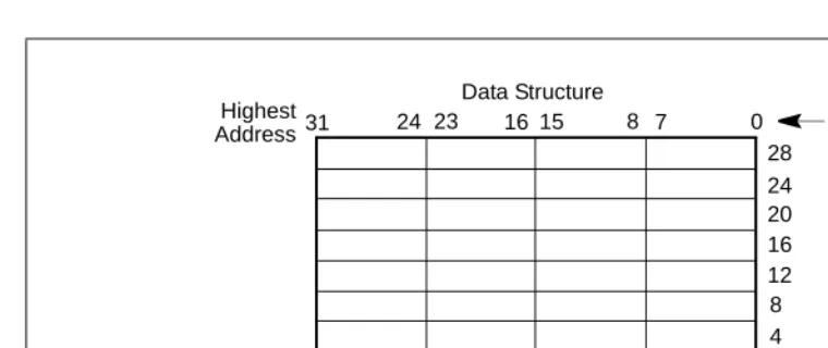
[image:25.612.48.428.77.237.2]Avoid any software dependence upon the state of reserved bits in IA-32 registers. Depending upon the values of reserved register bits will make software dependent upon the unspecified manner in which the processor handles these bits. Programs that depend upon reserved values risk incompat-ibility with future processors.
Figure 1-1. Bit and Byte Order Byte 3
Highest Data Structure
Byte 1
Byte 2 Byte 0
31 24 23 16 15 8 7 0
Address
Lowest Bit offset 28
24 20 16 12 8 4
0 Address
1-4 Vol. 2A
ABOUT THIS MANUAL
1.3.3
Instruction Operands
When instructions are represented symbolically, a subset of the IA-32 assembly language is used. In this subset, an instruction has the following format:
label: mnemonic argument1, argument2, argument3
where:
•
A label is an identifier which is followed by a colon.•
A mnemonic is a reserved name for a class of instruction opcodes which have the same function.•
The operands argument1, argument2, and argument3 are optional. There may be from zero to three operands, depending on the opcode. When present, they take the form of either literals or identifiers for data items. Operand identifiers are either reserved names of registers or are assumed to be assigned to data items declared in another part of the program (which may not be shown in the example).When two operands are present in an arithmetic or logical instruction, the right operand is the source and the left operand is the destination.
For example:
LOADREG: MOV EAX, SUBTOTAL
In this example, LOADREG is a label, MOV is the mnemonic identifier of an opcode, EAX is the destination operand, and SUBTOTAL is the source operand. Some assembly languages put the source and destination in reverse order.
1.3.4
Hexadecimal and Binary Numbers
Base 16 (hexadecimal) numbers are represented by a string of hexadecimal digits followed by the character H (for example, F82EH). A hexadecimal digit is a character from the following set: 0, 1, 2, 3, 4, 5, 6, 7, 8, 9, A, B, C, D, E, and F.
Base 2 (binary) numbers are represented by a string of 1s and 0s, sometimes followed by the character B (for example, 1010B). The “B” designation is only used in situations where confu-sion as to the type of number might arise.
1.3.5
Segmented Addressing
The processor uses byte addressing. This means memory is organized and accessed as a sequence of bytes. Whether one or more bytes are being accessed, a byte address is used to locate the byte or bytes in memory. The range of memory that can be addressed is called an address space.
ABOUT THIS MANUAL
refer to the code space, and stack addresses would always refer to the stack space. The following notation is used to specify a byte address within a segment:
Segment-register:Byte-address
For example, the following segment address identifies the byte at address FF79H in the segment pointed by the DS register:
DS:FF79H
The following segment address identifies an instruction address in the code segment. The CS register points to the code segment and the EIP register contains the address of the instruction.
CS:EIP
1.3.6
Exceptions
An exception is an event that typically occurs when an instruction causes an error. For example, an attempt to divide by zero generates an exception. However, some exceptions, such as break-points, occur under other conditions. Some types of exceptions may provide error codes. An error code reports additional information about the error. An example of the notation used to show an exception and error code is shown below.
#PF(fault code)
This example refers to a page-fault exception under conditions where an error code naming a type of fault is reported. Under some conditions, exceptions which produce error codes may not be able to report an accurate code. In this case, the error code is zero, as shown below for a general-protection exception.
#GP(0)
1.3.7
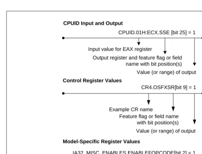
A New Syntax for CPUID, CR, and MSR Values
1-6 Vol. 2A
[image:28.612.44.441.81.383.2]ABOUT THIS MANUAL
Figure 1-2. Syntax for CPUID, CR, and MSR Data Presentation Control Register Values
Model-Specific Register Values
Input value for EAX register
CPUID.01H:ECX.SSE [bit 25] = 1
Value (or range) of output
CPUID Input and Output
Output register and feature flag or field name with bit position(s)
CR4.OSFXSR[bit 9] = 1
Feature flag or field name with bit position(s) Value (or range) of output Example CR name
Feature flag or field name with bit position(s) IA32_MISC_ENABLES.ENABLEFOPCODE[bit 2] = 1
Value (or range) of output Example MSR name
ABOUT THIS MANUAL
1.4
RELATED LITERATURE
Literature related to IA-32 processors is listed on-line at this link:
http://developer.intel.com/design/processor/
Some of the documents listed at this web site can be viewed on-line; others can be ordered. The literature available is listed by Intel® processor and then by the following literature types: appli-cations notes, data sheets, manuals, papers, and specification updates.
See also:
•
The data sheet for a particular Intel IA-32 processor•
The specification update for a particular Intel IA-32 processor•
AP-485, Intel Processor Identification and the CPUID Instruction, Order Number 2416181-8 Vol. 2A
CHAPTER 2
INSTRUCTION FORMAT
This chapter describes the instruction format for all IA-32 processors. The instruction format for protected mode, real-address mode and virtual-8086 mode is described in Section 2.1. Incre-ments provided for IA-32e mode and its sub-modes are described in Section 2.2
2.1
INSTRUCTION FORMAT FOR PROTECTED MODE,
REAL-ADDRESS MODE, AND VIRTUAL-8086 MODE
IA-32 instruction encodings are subsets of the format shown in Figure 2-1. Instructions consist of optional instruction prefixes (in any order), primary opcode bytes (up to three bytes), an addressing-form specifier (if required) consisting of the ModR/M byte and sometimes the SIB (Scale-Index-Base) byte, a displacement (if required), and an immediate data field (if required).
Figure 2-1. IA-32 Instruction Format Instruction
Prefixes Opcode ModR/M SIB Displacement Immediate
Mod OpcodeReg/ R/M 0 2
7 6 5 3
Scale Base
0 2
7 6 5 3
Index
Immediate data of 1, 2, or 4 bytes or none Address
displacement of 1, 2, or 4 bytes or none 1 byte
(if required) 1 byte
(if required) 1-, 2-, or 3-byte
opcode Up to four
prefixes of 1 byte each
2-2 Vol. 2A
INSTRUCTION FORMAT
2.1.1
Instruction Prefixes
Instruction prefixes are divided into four groups, each with a set of allowable prefix codes. For each instruction, one prefix may be used from each of four groups (Groups 1, 2, 3, 4) and be placed in any order.
•
Group 1— Lock and repeat prefixes:
•
F0H—LOCK•
F2H—REPNE/REPNZ (used only with string instructions; when used with the escape opcode 0FH, this prefix is treated as a mandatory prefix for some SIMD instructions)•
F3H—REP or REPE/REPZ (used only with string instructions; when used with the escape opcode 0FH, this prefix is treated as an mandatory prefix for some SIMD instructions)•
Group 2— Segment override prefixes:
•
2EH—CS segment override (use with any branch instruction is reserved)•
36H—SS segment override prefix (use with any branch instruction is reserved)•
3EH—DS segment override prefix (use with any branch instruction is reserved)•
26H—ES segment override prefix (use with any branch instruction is reserved)•
64H—FS segment override prefix (use with any branch instruction is reserved)•
65H—GS segment override prefix (use with any branch instruction is reserved)— Branch hints:
•
2EH—Branch not taken (used only with Jcc instructions)•
3EH—Branch taken (used only with Jcc instructions)•
Group 3•
66H—Operand-size override prefix (when used with the escape opcode 0FH, this is treated as a mandatory prefix for some SIMD instructions)•
Group 4INSTRUCTION FORMAT
The LOCK prefix (F0H) forces an operation that ensures exclusive use of shared memory in a multiprocessor environment. See “LOCK—Assert LOCK# Signal Prefix” in Chapter 3,
Instruc-tion Set Reference, A-M for a description of this prefix.
Repeat prefixes (F2H, F3H) cause an instruction to be repeated for each element of a string. Use these prefixes only with string instructions (MOVS, CMPS, SCAS, LODS, STOS, INS, and OUTS). Their use, followed by 0FH, is treated as a mandatory prefix by a number of SSE/SSE2/SSE3 instructions. Use of repeat prefixes and/or undefined opcodes with other IA-32 instructions is reserved; such use may cause unpredictable behavior.
Branch hint prefixes (2EH, 3EH) allow a program to give a hint to the processor about the most likely code path for a branch. Use these prefixes only with conditional branch instructions (Jcc). Other use of branch hint prefixes and/or other undefined opcodes with IA-32 instructions is reserved; such use may cause unpredictable behavior.
The operand-size override prefix allows a program to switch between 16- and 32-bit operand sizes. Either size can be the default; use of the prefix selects the non-default size. Use of 66H followed by 0FH is treated as a mandatory prefix by some SSE/SSE2/SSE3 instructions. Other use of the 66H prefix with MMX/SSE/SSE2/SSE3 instructions is reserved; such use may cause unpredictable behavior.
The address-size override prefix (67H) allows programs to switch between 16- and 32-bit addressing. Either size can be the default; the prefix selects the non-default size. Using this prefix and/or other undefined opcodes when operands for the instruction do not reside in memory is reserved; such use may cause unpredictable behavior.
2.1.2
Opcodes
A primary opcode can be 1, 2, or 3 bytes in length. An additional 3-bit opcode field is some-times encoded in the ModR/M byte. Smaller fields can be defined within the primary opcode. Such fields define the direction of operation, size of displacements, register encoding, condition codes, or sign extension. Encoding fields used by an opcode vary depending on the class of operation.
Two-byte opcode formats for general-purpose and SIMD instructions consist of:
•
An escape opcode byte 0FH as the primary opcode and a second opcode byte•
A mandatory prefix (66FH, F2H, F3H), an escape opcode byte, and a second opcode byte For example, CVTDQ2PD consists of the following sequence: F3 OF E6. The first byte is a mandatory prefix for SSE/SSE2/SSE3 instructions (it is not considered as a repeat prefix). Note that all three byte opcodes are reserved.2-4 Vol. 2A
INSTRUCTION FORMAT
2.1.3
ModR/M and SIB Bytes
Many instructions that refer to an operand in memory have an addressing-form specifier byte (called the ModR/M byte) following the primary opcode. The ModR/M byte contains three fields of information:
•
The mod field combines with the r/m field to form 32 possible values: eight registers and 24 addressing modes.•
The reg/opcode field specifies either a register number or three more bits of opcodeinfor-mation. The purpose of the reg/opcode field is specified in the primary opcode.
•
The r/m field can specify a register as an operand or it can be combined with the mod field to encode an addressing mode. Sometimes, certain combinations of the mod field and the r/m field is used to express opcode information for some instructions.Certain encodings of the ModR/M byte require a second addressing byte (the SIB byte). The base-plus-index and scale-plus-index forms of 32-bit addressing require the SIB byte. The SIB byte includes the following fields:
•
The scale field specifies the scale factor.•
The index field specifies the register number of the index register.•
The base field specifies the register number of the base register. See Section 2.1.5 for the encodings of the ModR/M and SIB bytes.2.1.4
Displacement and Immediate Bytes
Some addressing forms include a displacement immediately following the ModR/M byte (or the SIB byte if one is present). If a displacement is required; it be 1, 2, or 4 bytes.
INSTRUCTION FORMAT
2.1.5
Addressing-Mode Encoding of ModR/M and SIB Bytes
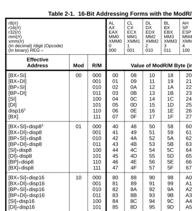
The values and corresponding addressing forms of the ModR/M and SIB bytes are shown in Table 2-1 through Table 2-3: 16-bit addressing forms specified by the ModR/M byte are in Table 2-1 and 32-bit addressing forms are in Table 2-2. Table 2-3 shows 32-bit addressing forms specified by the SIB byte. In cases where the reg/opcode field in the ModR/M byte represents an extended opcode, valid encodings are shown in Appendix B.
In Table 2-1 and Table 2-2, the Effective Address column lists 32 effective addresses that can be assigned to the first operand of an instruction by using the Mod and R/M fields of the ModR/M byte. The first 24 options provide ways of specifying a memory location; the last eight (Mod = 11B) provide ways of specifying general-purpose, MMX technology and XMM registers.
The Mod and R/M columns in Table 2-1 and Table 2-2 give the binary encodings of the Mod and R/M fields required to obtain the effective address listed in the first column. For example: see the row indicated by Mod = 11B, R/M = 000B. The row identifies the general-purpose regis-ters EAX, AX or AL; MMX technology register MM0; or XMM register XMM0. The register used is determined by the opcode byte and the operand-size attribute.
Now look at the seventh row in either table (labeled “REG =”). This row specifies the use of the 3-bit Reg/Opcode field when the field is used to give the location of a second operand. The second operand must be a general-purpose, MMX technology, or XMM register. Rows one through five list the registers that may correspond to the value in the table. Again, the register used is determined by the opcode byte along with the operand-size attribute.
If the instruction does not require a second operand, then the Reg/Opcode field may be used as an opcode extension. This use is represented by the sixth row in the tables (labeled “/digit (Opcode)”). Note that values in row six are represented in decimal form.
The body of Table 2-1 and Table 2-2 (under the label “Value of ModR/M Byte (in Hexadec-imal)”) contains a 32 by 8 array that presents all of 256 values of the ModR/M byte (in hexadec-imal). Bits 3, 4 and 5 are specified by the column of the table in which a byte resides. The row specifies bits 0, 1 and 2; and bits 6 and 7. The figure below demonstrates interpretation of one table value.
Figure 2-1. Table Interpretation of ModR/M Byte (C8H) Mod 00
RM 000 REG = 001
2-6 Vol. 2A
INSTRUCTION FORMAT
NOTES:
1. The default segment register is SS for the effective addresses containing a BP index, DS for other effec-tive addresses.
2. The disp16 nomenclature denotes a 16-bit displacement that follows the ModR/M byte and that is added to the index.
[image:38.612.56.432.80.492.2]3. The disp8 nomenclature denotes an 8-bit displacement that follows the ModR/M byte and that is sign-extended and added to the index.
Table 2-1. 16-Bit Addressing Forms with the ModR/M Byte
r8(/r) r16(/r) r32(/r) mm(/r) xmm(/r)
(In decimal) /digit (Opcode) (In binary) REG =
AL AX EAX MM0 XMM0 0 000 CL CX ECX MM1 XMM1 1 001 DL DX EDX MM2 XMM2 2 010 BL BX EBX MM3 XMM3 3 011 AH SP ESP MM4 XMM4 4 100 CH BP1 EBP MM5 XMM5 5 101 DH SI ESI MM6 XMM6 6 110 BH DI EDI MM7 XMM7 7 111 Effective
Address Mod R/M Value of ModR/M Byte (in Hexadecimal)
[BX+SI] [BX+DI] [BP+SI] [BP+DI] [SI] [DI] disp162 [BX] 00 000 001 010 011 100 101 110 111 00 01 02 03 04 05 06 07 08 09 0A 0B 0C 0D 0E 0F 10 11 12 13 14 15 16 17 18 19 1A 1B 1C 1D 1E 1F 20 21 22 23 24 25 26 27 28 29 2A 2B 2C 2D 2E 2F 30 31 32 33 34 35 36 37 38 39 3A 3B 3C 3D 3E 3F
[BX+SI]+disp83
[BX+DI]+disp8 [BP+SI]+disp8 [BP+DI]+disp8 [SI]+disp8 [DI]+disp8 [BP]+disp8 [BX]+disp8
01 000 001 010 011 100 101 110 111 40 41 42 43 44 45 46 47 48 49 4A 4B 4C 4D 4E 4F 50 51 52 53 54 55 56 57 58 59 5A 5B 5C 5D 5E 5F 60 61 62 63 64 65 66 67 68 69 6A 6B 6C 6D 6E 6F 70 71 72 73 74 75 76 77 78 79 7A 7B 7C 7D 7E 7F
[BX+SI]+disp16 [BX+DI]+disp16 [BP+SI]+disp16 [BP+DI]+disp16 [SI]+disp16 [DI]+disp16 [BP]+disp16 [BX]+disp16
INSTRUCTION FORMAT
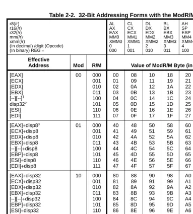
NOTES:
1. The [--][--] nomenclature means a SIB follows the ModR/M byte.
2. The disp32 nomenclature denotes a 32-bit displacement that follows the ModR/M byte (or the SIB byte if one is present) and that is added to the index.
[image:39.612.46.429.69.494.2]3. The disp8 nomenclature denotes an 8-bit displacement that follows the ModR/M byte (or the SIB byte if one is present) and that is sign-extended and added to the index.
Table 2-2. 32-Bit Addressing Forms with the ModR/M Byte
r8(/r) r16(/r) r32(/r) mm(/r) xmm(/r)
(In decimal) /digit (Opcode) (In binary) REG =
AL AX EAX MM0 XMM0 0 000 CL CX ECX MM1 XMM1 1 001 DL DX EDX MM2 XMM2 2 010 BL BX EBX MM3 XMM3 3 011 AH SP ESP MM4 XMM4 4 100 CH BP EBP MM5 XMM5 5 101 DH SI ESI MM6 XMM6 6 110 BH DI EDI MM7 XMM7 7 111 Effective
Address Mod R/M Value of ModR/M Byte (in Hexadecimal)
[EAX] [ECX] [EDX] [EBX] [--][--]1 disp322 [ESI] [EDI] 00 000 001 010 011 100 101 110 111 00 01 02 03 04 05 06 07 08 09 0A 0B 0C 0D 0E 0F 10 11 12 13 14 15 16 17 18 19 1A 1B 1C 1D 1E 1F 20 21 22 23 24 25 26 27 28 29 2A 2B 2C 2D 2E 2F 30 31 32 33 34 35 36 37 38 39 3A 3B 3C 3D 3E 3F
[EAX]+disp83
[ECX]+disp8 [EDX]+disp8 [EBX]+disp8 [--][--]+disp8 [EBP]+disp8 [ESI]+disp8 [EDI]+disp8
01 000 001 010 011 100 101 110 111 40 41 42 43 44 45 46 47 48 49 4A 4B 4C 4D 4E 4F 50 51 52 53 54 55 56 57 58 59 5A 5B 5C 5D 5E 5F 60 61 62 63 64 65 66 67 68 69 6A 6B 6C 6D 6E 6F 70 71 72 73 74 75 76 77 78 79 7A 7B 7C 7D 7E 7F
[EAX]+disp32 [ECX]+disp32 [EDX]+disp32 [EBX]+disp32 [--][--]+disp32 [EBP]+disp32 [ESI]+disp32 [EDI]+disp32
2-8 Vol. 2A
INSTRUCTION FORMAT
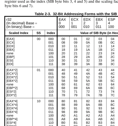
Table 2-3 is organized to give 256 possible values of the SIB byte (in hexadecimal). General purpose registers used as a base are indicated across the top of the table, along with corre-sponding values for the SIB byte’s base field. Table rows in the body of the table indicate the register used as the index (SIB byte bits 3, 4 and 5) and the scaling factor (determined by SIB byte bits 6 and 7).
NOTES:
1. The [*] nomenclature means a disp32 with no base if the MOD is 00B. Otherwise, [*] means disp8 or disp32 + [EBP]. This provides the following address modes:
[image:40.612.52.432.132.537.2]MOD bits Effective Address 00 [scaled index] + disp32 01 [scaled index] + disp8 + [EBP] 10 [scaled index] + disp32 + [EBP]
Table 2-3. 32-Bit Addressing Forms with the SIB Byte
r32
(In decimal) Base = (In binary) Base =
EAX 0 000 ECX 1 001 EDX 2 010 EBX 3 011 ESP 4 100 [*] 5 101 ESI 6 110 EDI 7 111
Scaled Index SS Index Value of SIB Byte (in Hexadecimal)
INSTRUCTION FORMAT
2.2
IA-32E MODE
IA-32e mode has two sub-modes. These are:
•
Compatibility Mode. Enables a 64-bit operating system to run most legacy protected mode software unmodified.•
64-Bit Mode. Enables a 64-bit operating system to run applications written to access 64-bit address space.2.2.1
REX Prefixes
REX prefixes are instruction-prefix bytes used in 64-bit mode. They do the following:
•
Specify GPRs and SSE registers.•
Specify 64-bit operand size.•
Specify extended control registers.Not all instructions require a REX prefix in 64-bit mode. A prefix is necessary only if an instruc-tion references one of the extended registers or uses a 64-bit operand. If a REX prefix is used when it has no meaning, it is ignored.
Only one REX prefix is allowed per instruction. If used, the prefix must immediately precede the opcode byte or the two-byte opcode escape prefix (if present). Other placements are ignored. The instruction-size limit of 15 bytes still applies to instructions with a REX prefix. See Figure 2-2.
Figure 2-2. Prefix Ordering in 64-bit Mode REX
Prefix Opcode ModR/M SIB Displacement Immediate
Immediate data of 1, 2, or 4 bytes or none Address
dis-placement of 1, 2, or 4 bytes or none
1 byte (if required) 1 byte (if
required) 1-, 2-, or
3-byte opcode (optional)
Grp 1, Grp 2, Grp 3, Grp 4 (optional)
2-10 Vol. 2A
INSTRUCTION FORMAT
2.2.1.1 Encoding
IA-32 instruction formats specify up to three registers by using 3-bit fields in the encoding, depending on the format:
•
ModR/M: the reg and r/m fields of the ModR/M byte•
ModR/M with SIB: the reg field of the ModR/M byte, the base and index fields of the SIB (scale, index, base) byte•
Instructions without ModR/M: the reg field of the opcodeIn 64-bit mode, these formats do not change. Bits needed to define fields in the 64-bit context are provided by the addition of REX prefixes.
2.2.1.2 More on REX Prefix Fields
REX prefixes are a set of 16 opcodes that span one row of the opcode map and occupy entries 40H to 4FH. These opcodes represent valid instructions (INC or DEC) in legacy IA-32 operating modes and in compatibility mode. In 64-bit mode, the same opcodes represent the instruction prefix REX and are not treated as individual instructions.
The single-byte-opcode form of INC/DEC instruction not available in 64-bit mode. INC/DEC functionality is still available using ModR/M forms of the same instructions (opcodes FF/0 and FF/1).
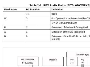
See Table 2-4 for a summary of the REX prefix format. Figure 2-3 though Figure 2-6 show examples of REX prefix fields in use. Some combinations of REX prefix fields are invalid. In such cases, the prefix is ignored. Some additional information follows:
•
Setting REX.W can be used to determine the operand size but does not solely determine operand width. Like the 66H size prefix, an REX 64-bit operand size override has no effect on byte-specific operations.•
For non-byte operations: if a 66H prefix is used with an REX prefix (REX.W = 1), 66H is ignored.•
If a 66H override is used with REX and REX.W = 0, the operand size is 16 bits.•
REX.R modifies the ModR/M reg field when that field encodes a GPR, SSE, control or debug register. REX.R is ignored when ModR/M specifies other registers or defines an extended opcode.•
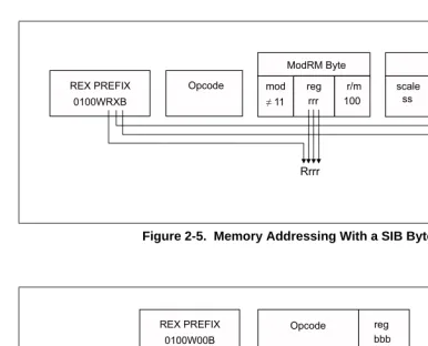
REX.X bit modifies the SIB index field.INSTRUCTION FORMAT
Table 2-4. REX Prefix Fields [BITS: 0100WRXB]
Field Name Bit Position Definition
- 7:4 0100
W 3 0 = Operand size determined by CS.D
1 = 64 Bit Operand Size
R 2 Extension of the ModR/M reg field
X 1 Extension of the SIB index field
B 0 Extension of the ModR/M r/m field, SIB base field, or Opcode
[image:43.612.47.430.71.358.2]reg field
Figure 2-3. Memory Addressing Without an SIB Byte; REX.X Not Used
Figure 2-4. Register-Register Addressing (No Memory Operand); REX.X Not Used
5(;35(),; :5%
2SFRGH PRG
UHJ UP
5UUU %EEE
0RG50%\WH
UUU EEE
20;ILJ
5(;35(),; :5%
2SFRGH PRG
UHJ UP
5UUU %EEE
0RG50%\WH
UUU EEE
2-12 Vol. 2A
INSTRUCTION FORMAT
In the legacy IA-32 architecture, byte registers (AH, AL, BH, BL, CH, CL, DH, and DL) are encoded in the ModR/M byte’s reg field, the r/m field or the opcode reg field as registers 0 through 7. REX prefixes provide an additional addressing capability for byte-registers that makes the least-significant byte of GPRs available for byte operations.
Certain combinations of the fields of the ModR/M byte and the SIB byte have special meaning for register encodings. For some combinations, fields expanded by the REX prefix are not decoded. Table 2-5 describes how each case behaves.
[image:44.612.50.437.76.388.2]Figure 2-5. Memory Addressing With a SIB Byte
Figure 2-6. Register Operand Coded in Opcode Byte; REX.X & REX.R Not Used
PRG
0RG50%\WH UP UHJ UUU
VFDOH VV
6,%%\WH 5(;35(),;
:5;%
2SFRGH
5UUU
EDVH
%EEE
EEE
;[[[
LQGH[ [[[
20;ILJ
5(;35(),; :%
2SFRGH
%EEE
UHJ EEE
INSTRUCTION FORMAT
2.2.1.3 Displacement
Addressing in 64-bit mode uses existing 32-bit ModR/M and SIB encodings. The ModR/M and SIB displacement sizes do not change. They remain 8 bits or 32 bits and are sign-extended to 64 bits.
Table 2-5. Special Cases of REX Encodings
ModR/M or SIB Sub-field Encodings Compatibility Mode Operation Compatibility
Mode Implications Additional Implications
ModR/M Byte mod != 11 SIB byte present. SIB byte required for ESP-based addressing.
REX prefix adds a fourth bit (b) which is not decoded (don't care). SIB byte also required for R12-based addressing. r/m ==
b*100(ESP)
ModR/M Byte mod == 0 Base register not used.
EBP without a displacement must be done using mod = 01 with displacement of 0.
REX prefix adds a fourth bit (b) which is not decoded (don't care). Using RBP or R13 without displacement must be done using mod = 01 with a displacement of 0. r/m ==
b*101(EBP)
SIB Byte index == 0100(ESP)
Index register not used.
ESP cannot be used as an index register.
REX prefix adds a fourth bit (b) which is decoded. There are no additional implications. The expanded index field allows distinguishing RSP from R12, therefore R12 can be used as an index.
SIB Byte base == 0101(EBP)
Base register is unused if mod = 0.
Base register depends on mod encoding.
REX prefix adds a fourth bit (b) which is not decoded.
This requires explicit displacement to be used with EBP/RBP or R13.
NOTES:
2-14 Vol. 2A
INSTRUCTION FORMAT
2.2.1.4 Direct Memory-Offset MOVs
In 64-bit mode, direct memory-offset forms of the MOV instruction are extended to specify a 64-bit immediate absolute address. This address is called a moffset. No prefix is needed to specify this 64-bit memory offset. For these MOV instructions, the size of the memory offset follows the address-size default (64 bits in 64-bit mode). See Table 2-6.
2.2.1.5 Immediates
In 64-bit mode, the typical size of immediate operands remains 32 bits. When the operand size is 64 bits, the processor sign-extends all immediates to 64 bits prior to their use.
Support for 64-bit immediate operands is accomplished by expanding the semantics of the existing move (MOV reg, imm16/32) instructions. These instructions (opcodes B8H – BFH) move 16-bits or 32-bits of immediate data (depending on the effective operand size) into a GPR. When the effective operand size is 64 bits, these instructions can be used to load an immediate into a GPR. A REX prefix is needed to override the 32-bit default operand size to a 64-bit operand size.
For example:
48 B8 8877665544332211 MOV RAX,1122334455667788H
2.2.1.6 RIP-Relative Addressing
A new addressing form, RIP-relative (relative instruction-pointer) addressing, is implemented in 64-bit mode. An effective address is formed by adding displacement to the 64-bit RIP of the next instruction.
In legacy IA-32 architecture, addressing relative to the instruction pointer is available only with control-transfer instructions. In 64-bit mode, instructions that use ModR/M addressing can use RIP-relative addressing. Without RIP-relative addressing, all ModR/M instruction modes address memory relative to zero.
RIP-relative addressing allows specific ModR/M modes to address memory relative to the 64-bit RIP using a signed 32-bit displacement. This provides an offset range of ±2GB from the RIP. Table 2-7 shows the ModR/M and SIB encodings for RIP-relative addressing. Redundant forms of 32-bit displacement-addressing exist in the current ModR/M and SIB encodings. There is one ModR/M encoding and there are several SIB encodings. RIP-relative addressing is encoded using a redundant form.
Table 2-6. Direct Memory Offset Form of MOV
Opcode Instruction
A0 MOV AL, moffset
A1 MOV EAX, moffset
A2 MOV moffset, AL
INSTRUCTION FORMAT
In 64-bit mode, the ModR/M Disp32 (32-bit displacement) encoding is re-defined to be RIP+Disp32 rather than displacement-only. See Table 2-7.
The ModR/M encoding for RIP-relative addressing does not depend on using an REX prefix. Specifically, the r/m bit field encoding of 101B (used to select RIP-relative addressing) is not affected by the REX prefix. For example, selecting R13 (REX.B = 1, r/m = 101B) with mod = 00B still results in RIP-relative addressing. The 4-bit r/m field of REX.B combined with ModR/M is not fully decoded. In order to address R13 with no displacement, software must encode R13 + 0 using a 1-byte displacement of zero.
RIP-relative addressing is enabled by 64-bit mode, not by a 64-bit address-size. The use of the address-size prefix does not disable RIP-relative addressing. The effect of the address-size prefix is to truncate and zero-extend the computed effective address to 32 bits.
2.2.1.7 Default 64-Bit Operand Size
In 64-bit mode, two groups of instructions have a default operand size of 64 bits (do not need a REX prefix for this operand size). These are:
•
Near branches•
All instructions, except far branches, that implicitly reference the RSP2.2.2
Additional Encodings for Control and Debug Registers
In 64-bit mode, more encodings for control and debug registers are available. The REX.R bit is used to modify the ModR/M reg field when that field encodes a control or debug register (see Table 2-4). These encodings enable the processor to address CR8-CR15 and DR8- DR15. An additional control register (CR8) is defined in 64-bit mode. CR8 becomes the Task Priority Register (TPR).
In the first implementation of IA-32e mode, CR9-CR15 and DR8-DR15 are not implemented. Any attempt to access unimplemented registers results in an invalid-opcode exception (#UD).
Table 2-7. RIP-Relative Addressing
ModR/M and SIB Sub-field Encodings
Compatibility Mode Operation
64-bit Mode Operation
Additional Implications in 64-bit mode
ModR/M Byte
mod == 00 Disp32 RIP + Disp32 Must use SIB form with
normal (zero-based) displacement addressing r/m == 101 (none)
SIB Byte base == 101 (none) if mod = 00, Disp32 Same as legacy
None
index == 100 (none)
2-16 Vol. 2A
3
CHAPTER 3
INSTRUCTION SET REFERENCE, A-M
This chapter describes the IA-32 instruction set (A-M) in IA-32e, protected, Virtual-8086, and real modes of operation. The set includes general-purpose, x87 FPU, MMX, SSE/SSE2/SSE3, and system instructions. The discussion continues in Chapter 4 for the balance of the instruction set (N-Z). See also Chapter 4, IA-32 Intel Architecture Software Developer’s Manual, Volume 2B. For each instruction, each operand combination is described. A description of the instruction and its operand, an operational description, a description of the effect of the instructions on flags in the EFLAGS register, and a summary of exceptions that can be generated are also provided.
3.1
INTERPRETING THE INSTRUCTION REFERENCE PAGES
This section describes the format of information contained in the instruction reference pages in this chapter. It explains notational conventions and abbreviations used in these sections.
3.1.1
Instruction Format
The following is an example of the format used for each instruction description in this chapter. The heading below introduces the example. The table below provides an example summary table.
CMC—Complement Carry Flag [Example Only]
3.1.1.1 Opcode Column in the Instruction Summary Table
The “Opcode” column in the table above shows the object code produced for each form of the instruction. When possible, codes are given as hexadecimal bytes in the same order in which they appear in memory. Definitions of entries other than hexadecimal bytes are as follows:
•
REX.W — Indicates the use of a REX prefix that affects operand size or instruction semantics. The ordering of the REX prefix and other optional/mandatory instruction prefixes are discussed Chapter 2, Instruction Format. Note that REX prefixes that promote legacy instructions to 64-bit behavior are not listed explicitly in the opcode column.Opcode Instruction 64-bit Mode
Compat/
Leg Mode Description
3-2 Vol. 2A
INSTRUCTION SET REFERENCE, A-M
•
/digit — A digit between 0 and 7 indicates that the ModR/M byte of the instruction uses only the r/m (register or memory) operand. The reg field contains the digit that provides an extension to the instruction's opcode.•
/r — Indicates that the ModR/M byte of the instruction contains a register operand and an r/m operand.•
cb, cw, cd, cp, co, ct — A 1-byte (cb), 2-byte (cw), 4-byte (cd), 6-byte (cp), 8-byte (co) or 10-byte (ct) value following the opcode. This value is used to specify a code offset and possibly a new value for the code segment register.•
ib, iw, id, io — A 1-byte (ib), 2-byte (iw), 4-byte (id) or 8-byte (io) immediate operand to the instruction that follows the opcode, ModR/M bytes or scale-indexing bytes. The opcode determines if the operand is a signed value. All words, doublewords and quadwords are given with the low-order byte first.•
+rb, +rw, +rd, +ro — A register code, from 0 through 7, added to the hexadecimal byte given at the left of the plus sign to form a single opcode byte. See Table 3-1 for the codes. The +ro columns in the table are applicable only in 64-bit mode.•
+i — A number used in floating-point instructions when one of the operands is ST(i) from the FPU register stack. The number i (which can range from 0 to 7) is added to the hexadecimal byte given at the left of the plus sign to form a single opcode byte.Table 3-1. Register Codes Associated With +rb, +rw, +rd, +ro
rb rw rd ro (64-Bit Mode only)
Regist er REX .R Reg F ield Regist er REX .R Reg F ield Regist er REX .R Reg F ield Regist er REX .R Reg F ield
AL 0 0 AX 0 0 EAX 0 0 RAX 0 0
CL 0 1 CX 0 1 ECX 0 1 RCX 0 1
DL 0 2 DX 0 2 EDX 0 2 RDX 0 2
BL 0 3 BX 0 3 EBX 0 3 RBX 0 3
AH No
REX prefix
4 SP No
REX prefix
4 ESP No
REX prefix
4 N/A N/A N/A
CH No
REX prefix
5 BP No
REX prefix
5 EBP No
REX prefix
5 N/A N/A N/A
DH No
REX prefix
6 SI No
REX prefix
6 ESI No
REX prefix
6 N/A N/A N/A
BH No
REX prefix
7 DI No
REX prefix
7 EDI No
REX prefix
INSTRUCTION SET REFERENCE, A-M
3.1.1.2 Instruction Column in the Opcode Summary Table
The “Instruction” column gives the syntax of the instruction statement as it would appear in an ASM386 program. The following is a list of the symbols used to represent operands in the instruction statements:
•
rel8 — A relative address in the range from 128 bytes before the end of the instruction to 127 bytes after the end of the instruction.•
rel16, rel32, rel64 — A relative address within the same code segment as the instruction assembled. The rel16 symbol applies to instructions with an operand-size attribute of 16 bits; the rel32 symbol applies to instructions with an operand-size attribute of 32 bits; the rel64 symbol applies to instructions with an operand-size attribute of 64 bits.•
ptr16:16, ptr16:32 and ptr16:64 — A far pointer, typically to a code segment different from that of the instruction. The notation 16:16 indicates that the value of the pointer has two parts. The value to the left of the colon is a 16-bit selector or value destined for the code segment register. The value to the right corresponds to the offset within theSPL Any
REX Prefix
4 SP 0 4 ESP 0 4 RSP 0 4
BPL