© 2015 IJSRSET | Volume 1 | Issue 2 | Print ISSN : 2395-1990 | Online ISSN : 2394-4099 Themed Section: Engineering and Technology
Design of Sequential Circuits Using MV Gates in Nanotechnology
Bahram Dehghan1, Ahad Salimi21
Department of Electrical Engineering, Sarvestan Branch, Islamic Azad University, Sarvestan, Iran 2Department of Electrical Engineering, Zarin dasht Branch, Islamic Azad University, Zarin dasht, Iran
ABSTRACT
Recent developments in reversible logic allow for improved quantum computer algorithms and schemes for corresponding computer architectures. Quantum dot Cellular Automata is an emerging technology for development of logic circuits based on nanotechnology, and it is one of the replacements for designing high performance computing over existing CMOS technology. Different logic gates like MV, NOT under QCA nanotechnology are introduced. Any Boolean functions, limited in thirteen number standard Boolean functions, are synthesized by MV and NNI gates or simply NNI gates alone, eliminating inverter (NOT) gate. The architecture of AND, OR, NAND, NOR gates by using MV gates have shown. Also, one of the other most applicable complete and efficient gates in digital systems and network are the XOR and XNOR gates. The design models of these gates have been exhibited. In this paper, we present the design of sequential circuits (RS Flip Flop, D Flip Flop, JK Flip Flop, T Flip Flop, Master Slave JK Flip Flop) and full subtractor/adder circuits based on MV gates and NOT gates. Furthermore, the number of gates and kind of them is considered.
Keywords: Sequential Circuit, MV Gates, Reversible Gate
I.
INTRODUCTION
Reversible logic has promising applications in the low power CMOS design, optical information processing, DNA computing, quantum computing and nanotechnology. It has many absorbing advantages such as smaller size, faster speed and low power consumption than transistor based technology. These circuits can produce single output vector from each input vector, and conversely, there was a one-to-one mapping between input and output vectors. Therefore, an NXN reversible gate can be shown as
Iv=(I1,I2,I3,I4,………IN) Ov=(O1,O2,O3,……….ON).
Where Iv and Ov can be shown the input and output vectors respectively. Classical logic gates are irreversible since input vector states cannot be uniquely reconstructed from the output vector states [1].
A quantum dot cellular automaton (QCA) is one of the practicable technologies to implement the sequential circuits.
QCA is a new technology for development of logic circuits based on nanotechnology, and it is one of the alternatives for designing high performance computing over existing CMOS technology[2]. QCA structures are polarization rather than the traditional current, contains the digital information. In this trend, instead of constructed as an array of quantum cells in which every cell has an electrostatic interaction with its neighboring cells. QCA applies a new form of computation, where interconnecting wires, the cells transfer the information throughout the circuit[3].
gates like MV, NOT under QCA nanotechnology to analyze sequential circuits. We have been proposed to achieve the best architecture of digital design with minimum gates.
II.
METHODS AND MATERIAL
A. Reversible Gate
Based on the observations from the previous section, Reversible logic is useful in mechanical applications of nanotechnology and the bijection (one-to-one
correspondence) between the input and output states which enables presumptive computations. In other words, any reversible gate must have the same number of input and output bits.
A logic gate L is reversible if, for any output Y, there is a unique input X such that
L(X) = Y (1) If gate L is reversible, there is an inverse gate L′ which
maps Y to X for which
L’(Y) = X (2) From common logic gates, NOT gate is reversible, as
can be seen from its truth table below[2].
Table1. Truth table NOT gate Input Output
0 1
1 0
In reversible logic there exists a one to one mapping between the inputs and the outputs vectors. In an irreversible circuit erasing a bit is equivalent to dissipation of kTln2 joules of heat energy where k is the Boltzmann’s constant and T is the absolute temperature of environment. If the operations are performed in reversible manner based on reversible logic circuits then there won’t be dissipation of kTln2 joules of heat energy[5]. So, it is significant to synthesize circuits with little energy consumption.
Figure.1. QCA cells showing how binary information is encoded in the two fully polarized diagonals of the cell[6].
Figure. 2. QCA majority gate.
Figure.3. QCA wire (90).
Figure. 4. QCA inverter. B. Sequential Circuits Using MV Gates
characteristics of QCA gates to generate AND, OR, NAND, NOR, EXOR, EXNOR gates. Secondly, According to the logic function of the majority gate, the designed optimum model of MV gates are put forward in conventional logic circuits in order to achieve equivalent circuits. However, The design of MV and NOT gates is further evaluated in implementing filip flop circuits.
For example, in order to make AND gate, one of the inputs of the MV majority gate can be set to zero. Similarly, for the OR gate, one of the inputs of the majority gate can be set to one. typical schemes are shown in the following figures.
Figure.5. Structure of NAND and NOR complete gates Also, Figure 6 displays the model of XOR gate in quantum dot cellular automata.
Figure.6. XOR gate design
The XOR gate represented in Fig.7. is basically equivalent to a first design, which may be seen differently resulted.
Figure.7. XOR gate design
It is the designed use of majority gates and inverters. Formula (4) presents the equation of this gate.
XOR = MV (MV (A, B,0),MV (Aʹ, Bʹ,0),1) (4)
Moreover, if we use NOT gate in output of Fig.7, we produce XNOR gate using that architecture. Another design that presented for XNOR gate is shown in Fig.8.
Figure.8. XNOR gate design
Also, it is the designed use of majority gates and inverters. Formula (5) presents the equation of this gate.
XNOR = MV (MV (A, B,0), (A+B)ʹ ,1) (5)
While realizing sequential circuits using MV gates,wire can implement as the basic schematic. This configuration is shown is Fig.9.
Figure.9. Wire using MV gates
In this section, we illustrate the application of the procedure using the following circuits.
a) RS FLIP FLOP
Figure 10. Conventional RS Flip Flop
Figure 11. Proposed evaluated circuit implementation using MV gates.
Another RS flip flop implementation using URG gate is presented in [9].
b)D FLIP FLOP
The D flip flop is a modification of the clocked RS flip flop. In the D flip flop, the D input goes directly to the S input and its complement is applied as an R input[8]. Figure 12 shows the D flip flop designed from conventional gates. The equivalent MV gates was proposed as indicated in Figure 13.
Figure 12. Conventional D Flip Flop
Figure 13. Proposed evaluated circuit implementation using MV gates.
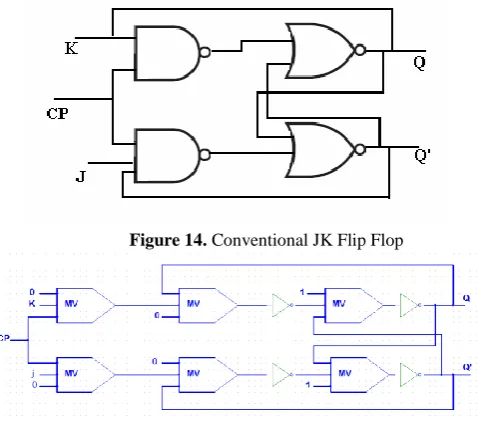
c) JK FLIP FLOP
A JK flip flop can be considered as a refinement of the RS flip flop since the indeterminate state of the RS type is defined in the JK type. The JK flip flop switches to its complement state, when inputs are applied to both J and K Simultaneously[8]. Figure 14 shows the JK flip flop designed from conventional gates. Figure 15 shows the JK flip flop designed from the equivalent MV gates.
Figure 14. Conventional JK Flip Flop
Figure 15. Proposed evaluated circuit implementation using MV gates.
d)T FLIP FLOP
The T(Toggle) flip-flop is obtained from the JK type if both inputs are tied together and are passed the same input signal. Figure 16 shows the T flip flop designed from conventional irreversible gates. The equivalent MV gates was proposed as indicated in Figure 18.
Figure 16. Conventional T Flip Flop
e) MASTER SLAVE FLIP FLOP
master and the other as a slave. Figure 17 shows the conventional master slave JK flip-flop constructed with NAND gates. . Figure 19 shows the Master Slave JK Flip Flop designed from the equivalent MV gates.
Figure 17. Conventional Master Slave JK Flip Flop
Figure 18. Proposed evaluated circuit implementation using MV gates.
Figure 19. Proposed evaluated circuit implementation using MV gates.
III.
RESULTS AND DISCUSSION
As discussed earlier, the simplified majority expression for the function is very important. The number of gates is different for each circuit as in some cases one circuit is able to serve ten MV gates. Table-2 shows the evaluation of the proposed circuits. By using MV and NOT gates we can produce filip flops profoundly.
Table 2. Evaluation of the proposed circuits
No of MV gates
No of NOT gates
Sum of gates
RS filip flop
4 2 6
D filip flop
4 5 9
JK filip flop
6 4 10
T filip flop
6 4 10
Master Slave JK filip flop
10 8 18
Full Subtractor/Adder
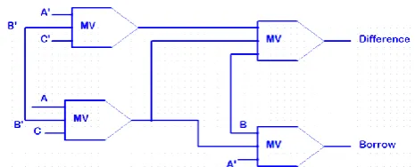
Also, We can implement a full subtractor using these majority gates.As shown in Fig.20, the number of majority gates has been reduced. Majority expression of full subtractor functions operator as Eq.6.
Borrow=MV(MV(A,B',C),MV(A',B,C),B) (6) Difference=MV(MV(A,B',C),MV(A',B,C),C')
Figure.20. Full Subtractor Circuit Diagram with 4 MV gates[10] Similarly, the other configuration is shown in fig.21. These functions are shown in Eq. 7.
Borrow=MV(MV(A,B',C),B,A') (7) Difference=MV(MV(A',B',C'),MV(A,B',C),B)
The above computation leads to another approach to design new structure based on MV gates.
than[10]. Recent results have been confirmed by the truth table. Further the introduced architecture can be extended to create more similar devices. In the current design, the mentioned equation(Eq. 8) is considered for 3 MV gates.
Borrow=MV(A',B,C) (8) Difference=MV(A,MV(A',B,C),MV(A',B',C')
The MV design of defined structure is shown in Fig.22.
Figure.22.Full Subtractor Circuit Diagram with 3 MV gates Another design of full subtractor is presented in Fig.23 The characteristic equation of the recent design can be written as:
Borrow=MV(A',B,C) (9) Difference=MV(MV(A',B,C),MV(A,B',C),C')
Figure.23. Full Subtractor Circuit Diagram with 3 MV gates Similarly the full adder circuit is designed and
implemented using QCA cells as shown in Fig.24. The characteristic equation of the recent design can be written as:
Carry=MV(A,B,C) (10) Sum=MV(MV(A,B,C'),(MV(A,B,C))',C)
Figure.24. Full Adder Circuit Diagram with 3 MV gates[11] According to [11], full adder function can be represented by 3 MV gates as shown in Fig.24.
By using (Eq. 11) , we obtain the simplified full adder expressions as follows:
Carry=MV(A,B,C) (11) Sum=MV(MV(A',B,C),(MV(A,B,C))',A)
Figure.25. Proposed full Adder Circuit Diagram with 3 MV gates Also, the circuit diagram for the corresponding circuit is shown in Fig.26.
Figure.27. Proposed Full Adder Circuit using using Quartus II simulator.
IV.
CONCLUSION
A lot of research has been accomplished in combinational as well as sequential design of reversible circuits. A quantum dot cellular automaton is an emerging field of research in nanotechnology. The proposed work focuses on the design of MV gates which are further used to design sequential circuits as a sample Flip Flops. Some designs based on MV gates including full adder, full Subtractor, RS filip flop, D filip flop, JK filip flop, T filip flop, Master Slave JK filip flop have been proposed in this research projects. In this paper, we had discussed the QCA technology which is becoming emerging technology in quantum computation. We had proposed different logic gate designs using MV gates. The result shows that logic synthesis using MV gates will be a promising step towards achieving the less gates in architecture. Ultimately, we can evaluate these designs with previous works to use the best approach.
V.
REFERENCES
[1] B. Dehghan, "Design of asynchronous sequential circuits using reversible logic gates", International Journal of Engineering and Technology, vol. 4, no. 4, pp. 213–219, 2012.
[2] Saroj Kumar Chandra, Prince Kumar Sahu," Basic Logic Gate Realization using Quantum Dot Cellular Automata based Reversible Universal Gate", International Journal of Computer Applications, Volume 58– No.18, pp.17-21, November (2012). [3] S. Karthigai Lakshmi, G. Athisha," Design and Analysis of
Subtractors using Nanotechnology Based QCA", European Journal of Scientific Research, Vol.53 No.4, pp.524-532, (2011).
[4] Bahram Dehghan, "Design Multipurpose Circuits with Minimum Garbage Outputs Using CMVMIN Gate," Chinese Journal of Engineering, Hindawi Publishing Corporation, Volume 2014.
[5] Saurabh Kotiyal, Himanshu Thapliyal , Nagarajan Ranganathan," Design of A Reversible Bidirectional Barrel
Shifter", 11th IEEE International Conference on Nanotechnology, pp.463-468, August (2011).
[6] Rumi Zhang, KonradWalus, WeiWang, Graham A. Jullien," A Method of Majority Logic Reduction for Quantum Cellular Automata", IEEE Transactions on Nanotechnology, VOL. 3, NO. 4, pp.443-450, December(2004).
[7] Himanshu Thapliyal, Nagarajan Ranganathan," Testable Reversible Latches for Molecular QCA", 8th IEEE Conference on Nanotechnology, pp.699-702, (2008).
[8] Himanshu Thapliyal, M.B Srinivas," A Beginning in the Reversible Logic Synthesisof Sequential Circuits", MAPLD International Conference, September (2005).
[9] Bahram Dehghan," Characterization and Logic Synthesis of URG gate for Designing Multipurpose Circuits", European Journal of Scientific Research,pp.117-125, July, (2013). [10]Bahram Dehghan,"Generating Subtractor Design by QCA Gates
under Nanotechnology", International Journal of Science and Engineering Investigations, Vol. 2, issue 14, pp.30-34, March (2013).
[11] Rumi Zhang, Konrad Walus, Wei Wang, Graham A. Jullien, "A Method of Majority Logic Reduction for Quantum Cellular
Automata", IEEE TRANSACTIONS ON
![Figure.1. QCA cells showing how binary information is encoded in the two fully polarized diagonals of the cell[6]](https://thumb-us.123doks.com/thumbv2/123dok_us/1164104.1618748/2.595.364.496.52.158/figure-cells-showing-binary-information-encoded-polarized-diagonals.webp)