University of Windsor University of Windsor
Scholarship at UWindsor
Scholarship at UWindsor
Electronic Theses and Dissertations Theses, Dissertations, and Major Papers
2011
A Low Power Multiple Valued Logic SRAM Cell Using Single
A Low Power Multiple Valued Logic SRAM Cell Using Single
Electron Devices
Electron Devices
Naila Syed
University of Windsor
Follow this and additional works at: https://scholar.uwindsor.ca/etd
Recommended Citation Recommended Citation
Syed, Naila, "A Low Power Multiple Valued Logic SRAM Cell Using Single Electron Devices" (2011). Electronic Theses and Dissertations. 144.
https://scholar.uwindsor.ca/etd/144
This online database contains the full-text of PhD dissertations and Masters’ theses of University of Windsor students from 1954 forward. These documents are made available for personal study and research purposes only, in accordance with the Canadian Copyright Act and the Creative Commons license—CC BY-NC-ND (Attribution, Non-Commercial, No Derivative Works). Under this license, works must always be attributed to the copyright holder (original author), cannot be used for any commercial purposes, and may not be altered. Any other use would require the permission of the copyright holder. Students may inquire about withdrawing their dissertation and/or thesis from this database. For additional inquiries, please contact the repository administrator via email
A LOW POWER MULTIPLE VALUED LOGIC SRAM
CELL USING SINGLE ELECTRON DEVICES
by
Naila Syed
A Thesis
Submitted to the Faculty of Graduate Studies through Electrical and Computer Engineering in Partial Fulfillment of the Requirements for
the Degree of Master of Science at the University of Windsor
Windsor, Ontario, Canada
2011
A LOW POWER MULTIPLE VALUED LOGIC SRAM
CELL USING SINGLE ELECTRON DEVICES
by
Naila Syed
APPROVED BY:
______________________________________________ Dr. Huiming Zhang
Department of Biological Sciences
______________________________________________ Dr Huapeng Wu
Department of Electrical and Computer Engineering
______________________________________________ Dr. Chunhong Chen, Advisor
Department of Electrical and Computer Engineering
______________________________________________
Dr. M. Mirhassani, Chair of Defense
Department of Electrical and Computer Engineering
iii
Author’s Declaration of Co-Authorship / Previous Publication
I. Co-Authorship Declaration
I hereby declare that this thesis incorporates material that is result of joint research, as
follows:
In all cases, the primary contributions, derivations, experimental setup, data analysis and
interpretation were performed by the author through the supervision of Dr. C. Chen. In
addition to supervision, Dr. C. Chen provided the author with the project idea, guidance,
and financial support.
I am aware of the University of Windsor Senate Policy on Authorship and I certify that I
have properly acknowledged the contribution of other researchers to my thesis, and have
obtained written permission from the co-author to include the above material(s) in my
thesis.
I certify that, with the above qualification, this thesis, and the research to which it refers,
is the product of my own work.
II. Declaration of Previous Publication
This thesis includes two original paper that have been previously published/submitted for
iv Thesis
Chapter
Publication title/full citation Publication status*
Chapter 4 N.Syed and C.Chen, ―Low Power
SET-Based SRAM Cell Design Using
Negative Differential Conductance‖, in
Proc. of IEEE-Nano'11 , pp. 744-747,
August 2011, Portland, Oregon, USA.
―Published‖
Chapter 4,5 N.Syed and C.Chen, ―Low Power
SET-Based SRAM Cells for Binary and
Multiple-Valued Logic‖
―To be submitted‖ for
publication
I certify that I have obtained a written permission from the copyright owner to include the
above published material in my thesis. I certify that the above material describes work
completed during my registration as graduate student at the University of Windsor.
I declare that, to the best of my knowledge, my thesis does not infringe upon anyone‘s
copyright nor violate any proprietary rights and that any ideas, techniques, quotations, or
any other material from the work of other people included in my thesis, published or
otherwise, are fully acknowledged in accordance with the standard referencing practices.
Furthermore, to the extent that I have included copyrighted material that surpasses the
bounds of fair dealing within the meaning of the Canada Copyright Act, I certify that I
have obtained a written permission from the copyright owner to include such material(s)
v
I declare that this is a true copy of my thesis, including any final revisions, as approved
by my thesis committee and the Graduate Studies office, and that this thesis has not been
vi
Abstract
It is widely known that the decreasing feature size facilitated vast improvement
in semiconductor-based design. The scaling down of MOS transistors has almost come to
an end due to the limits dictated by their operating principle. In order to ensure further
feature size reduction, the field of single-electronics has been developed. Single Electron
Tunnelling (SET) technology offers the ability to control the transport and position of a
single or a small number of electrons.
This thesis investigates the power optimisation of single electron memory based
on negative differential conductance (NDC) characteristic. A novel SET-based NDC
architecture with multiple peaks in I-V characteristic is introduced. Two specific static
random-access memory (SRAM) cells are proposed: (i) a ternary SRAM with a standby
power consumption of 0.98nW at logic margin of 270mV and (ii) a quaternary SRAM
cell with standby power consumption of 5.06 at a logic margin of 160 mV operating at
T=77K.. The read/write operations for the memory cell are briefly discussed. All
A Sincere Dedication
To mummy, daddy, hubby and my baby Amaan with love...
It is your support and love that keeps me going.
Acknowledgements
Before all, I thank Almighty Allah who has always guided me and blessed me
with all the lovely people in my life who have supported and encouraged me at every
step to make this work possible.
With utmost sincerity I express my gratitude and respect to my advisor Dr.
Chunhong Chen, who has always inspired me to work with honesty, integrity and
discipline. His guidance and reassuring aura have been indispensible boons contributing
to the completion of this thesis. I am thankful to Guoqing Deng for his helpful comments
and encouraging words all the time. This note would be incomplete without thanking
Andria Ballo for her ever-readiness to help and valuable guidance.
I would never be here without the love, support and encouragement of Mom and
Dad. I always wish that I can be as perfect as you both are. Not to forget Didi, Rabi,
Ninna, my little bro Bu and my ever supportive husband, Hamed .Thank you guys for
being there for me always. And of course, thank you, my baby Amaan for your great big
hugs that completely make me forget about my stress.
Last, but not the least I would like to thank all my friends, especially Amna,
Shaima and Bhabi for all their support and encouragement throughout the course of my
Table of Contents
Author‘s Declaration of Previous Publication ... iii
Abstract ... vi
A Sincere Dedication ... vii
Acknowledgements ... viii
List of Tables ... xi
List of Figures ... xii
List of Abbeviations ... xiv
CHAPTER I. INTRODUCTION 1.1 Background and Motivation ...1
1.2 Thesis organisation...6
II. SINGLE ELECTRON TUNNELLING BACKGROUND 2.1 Single Electronics and Coulomb Blockade ...8
2.2 Condition for Coulomb Blockade ...10
2.3 Reliability issues of SET ...13
2.3.1 Operating temperature ...13
2.3.2 Random Background Charge ...14
2.4 Monte Carlo Simulator for SET (SIMON ) ...15
III. SRAM DESIGN METHODOLOGY USING SINGLE ELECTRON DEVICES EXHIBITING NDC 3.1 NDC blocks based on single electron devices ...16
3.1.1 NDC Block 1 ...16
3.1.2 NDC Block 2 ...18
3.1.3 NDC Block 3 ...20
3.2 SRAM structure using NDC elements ...21
3.3 SET based READ/WRITE switch ...23
3.5 SRAM Cell based on single electron NDC elements ...28
3.4.1 SRAM cell A...28
3.4.2 SRAM cell B ...32
IV. STANDBY POWER OPTIMISATION TECHNIQUE FOR STATIC MEMORY CELL 4.1 Optimisation Methodology ...36
4.2 Effect of Temperature and Random background charge ...39
V. A NOVEL SET BASED ELEMENT WITH MULTIPLE PEAK NDC 5.1 Multiple peak NDC architecture ...43
5.2 Mechanism for multiple NDC peaks ...44
5.3 Effect of Temperature and Background charge ...46
5.4 A Novel MVL SRAM cell based on single electron devices ...47
5.5 Standby power optimisation of MVL SRAM cell ...52
5.6 A Novel Quaternary SRAM cell ...55
VI. RESULTS AND DISCUSSIONS………..57
VII. CONCLUSIONS AND FUTURE WORK 7.1 Conclusion………60
7.2 Future work ...60
REFERENCES ...62
APPENDIX A : PERMISSION FROM CO -AUTHOR ...65
List of Tables
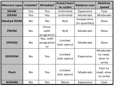
1.1 Comparison of different memory types ...4
3.1 Parameters for load and driving NDC Blocks ...28
3.2 Logic state for different values of Input voltage Vds ...31
3.3 Performance metrics for SRAM Cell of Fig 3.11 ...31
3.4 Parameters for load and driving NDC Blocks ...33
3.5 Logic state for different values of Input voltage Vds ...33
3.6 Performance metrics for SRAM Cell of Fig 3.14 ...35
3.7 Performance metrics for SRAM Cell of Fig 3.11 ...35
5.1 (a) Parameters for the Multiple peak static memory cell (b) Parameters for write switch ...49
5.2 Parameters for the Quaternary memory NDC elements ...55
6.1 Comparison of SET based SRAM cell l ...57
List of Figures
1.1 Feature size reduction within the last 3 decades ...2
1.2 Classification of memory types ...3
1.3 Negative Differential resistance characteristic curve ...5
2.1 Equivalent circuit for double tunnel junction ...11
2.2 IV characteristic for double tunnel junction ...13
2.3 Interface of Monte Carlo simulator SIMON ...15
3.1 Schematic diagram SET block 1 exhibiting NDC ...17
3.2 IV characteristic of SET block 1 ...17
3.3 Schematic diagram SET block 2 exhibiting NDC ...19
3.4 IV characteristic of SET block 2 ...19
3.5 Schematic diagram SET block 3 exhibiting NDC ...20
3.6 IV characteristic of SET block 3 ...21
3.7 Schematic Diagram for NDC based SET memory cell ...22
3.8 Load lines of driving and load SET block ...22
3.9 SET transistors for (a)WRITE and (b) READ ...24
3.10 Memory write input and read output waveforms: (a) input data; (b) write switch; (c) voltage on memory node ...25
3.11 Schematic of SRAM cell using NDC element from Section 3.2.3 ...29
3.12 Load Line diagram for SRAM cell using NDCelement from Section 3.2.3 ...30
3.13 Stable voltages are at 150mV and 400mV ...30
3.14 Schematic of SRAM cell using NDC element from Section 3.2.2 ...32
3.15 Two stable voltages are at 110mV and 230mV ...34
4.1 Standby power vs. gate capacitance for memory cell using NDCs of [5] ...37
4.2 Logic margin vs. gate capacitance for memory cell using NDCs of [5]. ...38
4.3 Standby power vs. logic margin for memory cell using NDCs of [5]. ...38
4.4 Logic margin vs. standby power at different temperatures ...39
4.5 Logic margin vs. standby power at different background charges ...40
5.1 Proposed multiple peak Set based NDC architecture ...43
5.2 I–V characteristics for the multiple peak SET block ...44
5.3 Probable electron charge configuration ...46
5.4 Effect on temperature on the multiple peaks NDC ...46
5.5 Effect on Random background charge on the multiple peak NDC ...47
5.7 Load line diagram for memory cell using two peak NDC element ...50
5.8 Memory voltages (a) input (b) write (c) memory node ...51
5.9 Standby power vs. Logic margin for the ratio Cg/Ct =2 ...52
5.10 Standby power vs. temperature at Ct=0.2aF for Cg/Ct=2 ...53
5.11 Standby power vs. Logic margin for the ratio Cg/Ct =3 at T=77K ...53
5.12 Load line diagram NDC element for Ct = 0.1aF with ratio Cg/Ct=3 ...54
5.13 IV characteristic for three peak NDC of Quaternary cell ...55
List of Abbreviations
CMOS -- Complementary Metal Oxide Semiconductor
DRAM -- Dynamic Random Access Memory
HFET – Hetero structure Field Effect Transistor
LSI -- Large Scale Integration
MOSFET – Metal Oxide Semiconductor Field Effect Transistor
MVL – Multiple Valued Logic
NDC – Negative Differential Conductance
PVCR – Peak to Valley Current Ratio
RAM – Random Access Memory
ROM – Read Only Memory
RTD -- Resonant Tunneling Diode
SED – Single Electron Device
SET -- Single Electron Transistor
CHAPTER I:
INTRODUCTION
This chapter starts with a clear definition of the issue this research work
addresses, explaining the importance of the work and its outcomes. Section 1.1 gives us
some background for need for single electron technology and SRAM memory. Finally
Section 1.2 briefly explains the organisation of this thesis.
1.1
BACKGROUND AND MOTIVATION
The rapid growth of the semiconductor industry over the past three decades has
largely been enabled by continual advancements in manufacturing technology which
have allowed the size of the transistor, the basic building block in integrated circuits (ICs)
, to be steadily reduced with each new generation of technology .As the transistor size is
scaled down, the chip area required for a given circuit is reduced, so that more chips can
be manufactured on a single silicon wafer substrate, resulting in lower manufacturing
cost per chip. Circuit operation speed also improves, because of reduced capacitance and
higher transistor current density. Fabrication facilities presently manufacture ICs with
minimum transistor lithographically defined feature size smaller than 100nm, so that the
microprocessor products with transistor counts approaching 100 million transistors per
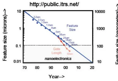
chip can be manufactured cost effectively. Figure 1.1 shows the shrinking feature size
with every decade .The scale-down of the size of MOSFET transistors has so far reached
deep sub-50nm regime beyond which physical limits are introduced such as quantum
rapidly increasing power dissipation due to ever larger numbers of transistors and high
levels of interconnections that is pushing CMOS circuits beyond their cooling limit.
Achieving low power operation of LSIs requires reduction in the total capacitance of
circuits and operation voltage, which reduces the number of electrons participating in the
operation of some unit instruction.
Figure 1.1: Feature size reduction within the last 3 decades. (International
Technology Roadmap for Semiconductors. http://public.itrs.net/)
Single-electron devices (SEDs) [2–4], which literally have potential to manipulate
electrons on the level of elementary charge, are thus considered to be the devices that will
allow such a change. In addition to their low-power nature, SEDs have a rather simple
device size is reduced to the molecular level. In addition, their performance improves as
they become smaller. These properties are quite beneficial for large-scale integration
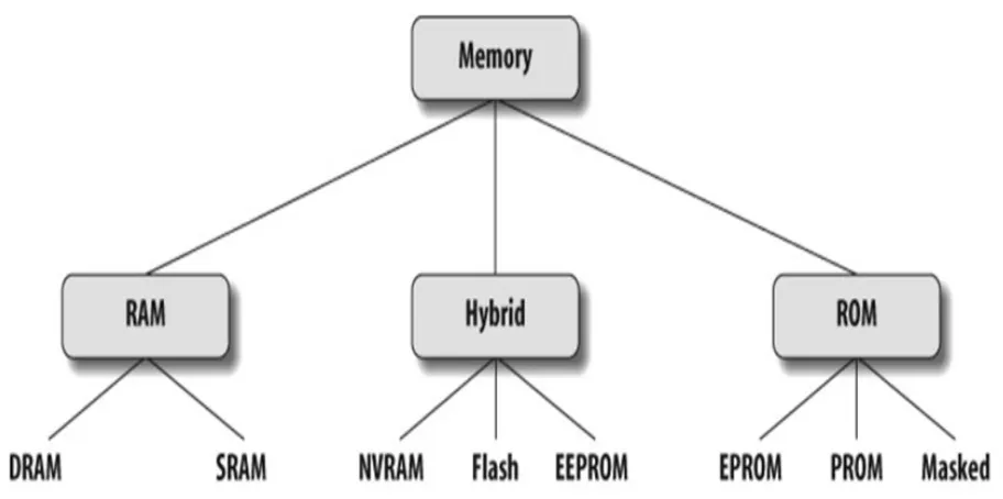
Many types of memory devices are available for use in modern computer systems
Fig 1.2 shows that memory is broadly categorized as RAM, ROM and Hybrid. Data
stored in RAM is volatile and is retained as long as power is applied to the
chip.
Figure 1.2: Classification of memory types
Data can be rewritten infinite number of times. In ROM, information once written
is retained forever, even when power is removed. Information may be rewritten a few
times but only by manufacturer or programmer. Hybrid memory shares the features of
Table 1.1: Comparison of different memory types
The RAM family includes two important memory devices: static RAM (SRAM)
and dynamic RAM (DRAM). The DRAM memory cell consists of a single pass transistor
and a capacitor (1T/1C) wherein information is stored in the form of a charge on the
capacitor .Although the DRAM cell provides the most compact layout it requires frequent
refreshing (typically on the order of once per millisecond) because the charge on the
capacitor leaks away at the rate of approximately 10-15 Amperes per cell. This problem is
exacerbated by technology scaling because the transistor leakage current increases with
decreasing channel length, and also because a reduction in a cell capacitance results in a
small number of stored carriers, so that more frequent refreshing is necessary. Static
the SRAM cell is more complex. Presently a CMOS SRAM cell requires either four
n-channel metal-oxide-semiconductor field effect transistors (MOSFETs) and two
p-channel MOSFETs or four n-p-channel MOSFETs and two polycrystalline silicon(poly-Si)
load resistors, resulting in significantly larger cell size .Innovations which provide
significant reductions in SRAM cell while allowing the SRAM cell to retail favourable
operating characteristics are therefore highly desirable.
Negative differential conductance (NDC) devices have previously been proposed
for compact static memory applications. E. Goto [11] disclosed an SRAM cell consisting
of two resonant tunnel diodes (RTDs) and a single pass transistor .For a variety of NDC
devices including RTDs, the current first increases with increasing applied voltage,
reaching a peak value, then decreases with increasing applied voltage over a range of
applied voltages, exhibiting negative differential conductance over this range and
reaching a minimum value (valley ).At yet higher applied voltage the current again
increases with increasing applied voltage .Thus the current –vs.-voltage characteristic is
shaped like the letter ‗N‘.
A figure of merit for NDC devices is the ratio of the peak current to valley current
(PVCR). The PVCR of RTDs is generally not high enough to make it practical for low
power SRAM application, because in order for the RTD to have sufficient current drive,
the valley current is too large, causing large static power dissipation.
There exist only a few reports concerning different cells of SETs exhibiting NDC
[3-5]. In 1999, Heij et al. [3] reported on NDC effects in SETs for the first time, but the
design was not suitable for memory application due very small operating voltage range.
Later an NDR cell composed of two cross-connected SETs was presented by Mahapatra
and Ionescu [4] followed by another interesting NDC element reported by Lee and Jeong
[5] in 2004. These designs even though suitable for memory application were not
optimised for low standby power consumption.
Accordingly there exists a significant need for SET based NDC devices with a
low standby power consumption and good PVCR suitable for low power, low cost
SRAM. Another reason for emphasizing on memory based on NDC devices is to be able
to design SET based cell that exhibit multiple peaks in NDC characteristic since there
have been no reports on SET based architecture that exhibits multiple peak NDC
characteristic suitable for use for multiple valued logic (MVL) Static memory cell.
1.2
THESIS ORGANISATION
This thesis is organized as follows. Chapter 2 provides a background on the
Later some basic information is presented for the Monte Carlo simulator for SET
SIMON.
Chapter 3 presents a few proposed SET cells exhibiting NDC characteristic and
clearly explains the methodology to build a SRAM cell using two similar NDC elements.
The performance metrics of such a design are highlighted and discussed briefly. A read
/write circuit based on single electron oscillation property is also introduced which is
used throughout for simulation in SIMON. SRAM cell are implemented using the
available SET based NDC elements and compared based on the performance.
Chapter 4 deals with an optimisation technique for low standby power
consumption with a good compromise between logic margin. In chapter 5, we propose a
novel SET architecture exhibiting multiple peaks in NDC characteristic and implement
its application as a low power Multiple valued logic (MVL ) SRAM cell. Further
discussions on optimisation of this design and effect of temperature and background
charges are carried out.
In Chapter 6, all the results are compared and analysed based on performance
CHAPTER II
SINGLE ELECTRON TUNNELLING BACKGROUND
2.1 SINGLE ELECTRONICS AND COULOMB BLOCKADE
To have basic understanding single electron devices, we need to review the basic
physical mechanism involved in these devices. Single electron devices are based on the
phenomenon of coulomb blockade involving the classical effect of repulsion between like
charges [26]. The energy that determines the transport of electrons through a single
electron device is Helmholtz's free energy, F, which is defined as difference between total
energy, EΣ , stored in the device and work done by power sources, W. The total energy
stored includes all components that have to be considered when charging an island with
an electron.
F = EΣ – W (2.1)
EΣ = EC + ΔEF + EN (2.2)
The change in Helmholtz's free energy a tunnel event causes is a measure of the
probability of this tunnel event. The general fact that physical systems tend to occupy
lower energy states, is apparent in electrons favouring those tunnel events which reduce
the free energy. The components of EΣ are:
2.1.1 Electron Electron Interaction, EC
An entirely classical model for electron-electron interaction is based on the
every additional charge dq which is transported to a conductor, work has to be done
against the field of already present charges residing on the conductor. Charging an island
with capacitance C with an electron of charge e requires
(2.3)
2.1.2 Fermi Energy, ΔEF
Systems with sufficiently small islands are not adequately described with the
above classical model alone. They exhibit second electron-electron interaction energy,
namely the change in Fermi energy, when charged with a single electron.
2.1.3 Quantum Confinement Energies, E N
With decreasing island size the energy level spacing of electron states increases
indirectly proportional to the square of the dot size. Taking an infinite potential well as a
simple model for a quantum dot, one calculates by solving Schrödinger's equation
(2.4)
2.1.4 Work Done by Voltage Sources, W
To evaluate the available energy for a given tunnel event, the work done on the
system by the power supplies has to be included, since thermodynamically the interacting
islands represent an open system. The work done by the voltage sources may be written
(2.5)
2.
2 CONDITION FOR COULOMB BLOCKADE
Minimum tunnel resistance for single electron charging is
(2.6)
The thermal kinetic energy of the electron must be less than the Coulomb repulsion
energy which will lead to reduction in current leading to blockade.
kT < EC (2.7)
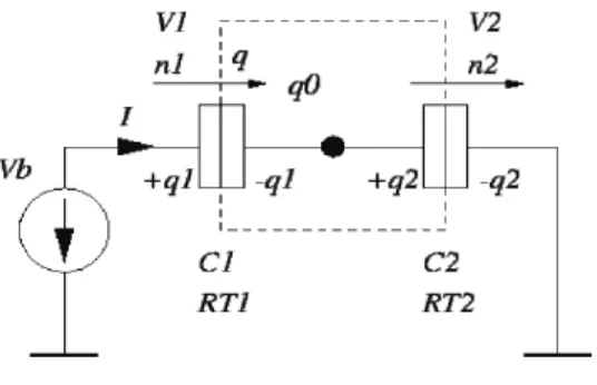
Consider two tunnel junctions in series biased with an ideal voltage source as shown in
Fig. 2.1. The charges on junction one, junction two, and on the whole island can be
written as
q1 = C1V1 , q2 = C2V2 , q = q2 − q1 + q0 = − ne + q0 (2.8)
n1 the number of electrons that tunnelled through the first junction entering the island, n2
the number of electrons that tunnelled through the second junction exiting the island, and
Figure 2.1: Equivalent circuit for double tunnel junction
A background charge q0 produces generally a non-integer charge offset. The
background charge is induced by stray capacitances that are not shown in the circuit
diagram Fig 2.1 and impurities located near the island, which are practically always
present. Using (2.8) and
Vb=V1+V2 (2.9)
gives
(2.10)
The electrostatic energy stored in the double junction is
(2.11)
In addition, to get the free energy one must consider the work done by the voltage
this electron, plus the change in polarization charge caused by the tunnelling electron. V1
changes according to (2.10) by –e/ CΣ and hence the polarization charge is –e C1/ CΣ. The
charge q1 gets smaller, which means that the voltage source receives polarization charge.
The total charge that has to be replaced by the voltage source is therefore –e C1/ CΣ and
the work done by the voltage source in case electrons tunnel through junction 1 and
junction 2 is accordingly
(2.12)
Thus, the free energy of the complete circuit is
(2.13)
The change in free energy for an electron tunnelling through junction 1 and 2 is
given by
(2.14)
(2.15)
The probability of a tunnel event will only be high, if the change in free energy is
negative - a transition to a lower energy state. The leading term in (2.14) and (2.15)
causes ΔF to be positive until the magnitude of the bias voltage Vb exceeds a threshold
which depends on the smaller of the two capacitances. This is the case for all possible
(C1=C2) the condition becomes Vb > e /CΣ. This suppression of tunnelling for low bias is
the Coulomb blockade. Figure 2.2 shows IV characteristic for double tunnel junction
The solid line gives characteristic for q0 =0 and the dashed line for q0 =0.5e .Coulomb
blockade is a direct result of additional coulomb energy e2 = 2C which must be expended
by an electron in order to tunnel into or out of an island
Figure 2.2: IV characteristic for double tunnel junction.
2.3 RELIABILITY ISSUES OF SET
2.3.1 OPERATING TEMPERATURE
Needless to say only when room temperature operation is achieved will
single-electron devices have a noticeable impact. Liquid nitrogen operation temperature is only
acceptable for certain special applications. Room temperature operation is only possible
with feature sizes below 10 nm, which is today only achievable with granular production
techniques. New material systems which have lower dielectric permittivity or exhibit
spatial restriction noticeable. Unfortunately, new materials very often require new
processes which have to be developed and studied. This takes a lot of time and research
effort. Hence the economical factor limits this possibility drastically. Another factor for
the maximum operation temperature is the affordable error rate. In single-electron logic
devices error rates strongly depend on the temperature. If the thermal energy, kBT, is
larger or of equal magnitude than the Coulomb energy, no sensible operation is usually
possible.
2.3.2 RANDOM BACKGROUND CHARGE
This term denotes any charge which is located close enough to the circuit to be
disturbing, but which is outside of our direct control, making it virtually random. These
are charged impurities, traps, parasitic and stray capacitances and other circuit parts,
which may induce charges on sensitive quantum dots. Single-electron devices are
extremely charge sensitive, which can be exploited for highly sensitive electrometers, but
which is in most devices a deadly feature, destroying desired device functions. Currently
there are two approaches under investigation, which deal with this problem. One
possibility is to find process technologies which allow production of impurity free
materials or materials where impurities accumulate in regions where they are not
disturbing device behaviour. A second approach is to use SET features which are
2.4 MONTE CARLO SIMULATOR FOR SET (SIMON)
All our simulations in the following chapters are carried out using the Monte
Carlo method. SIMON is a single-electron tunnel device and circuit simulator [12]. It
allows transient and stationary simulation of arbitrary circuit consisting of tunnel
junctions, capacitors, and voltage sources of three kinds: constant, piecewise linearly time
dependent, and voltage controlled. A graphic user interface allows the quick and easy
design of circuits with single-electron tunnel devices. Parameters can be changed
interactively, and simulation results can be looked at in graphical form. Also, all
simulation parameters such as simulation mode, event number, and temperature, are
modifiable. Fig 2.3 shows the interface of SIMON.
CHAPTER III
SRAM DESIGN METHODOLOGY USING
SINGLE ELECTRON DEVICES EXHIBITING
NDC
This chapter compares different negative differential blocks based on single
electron devices in Section 3.1. The methodology to construct static RAM cell using
NDC elements is presented in section 3.2. A read/write circuit based on Coulomb
oscillations that is used throughout our research simulations is presented in section 3.3.
Section 3.4 highlights the different performance metrics in SRAM cell. In section 3.5
SET based static memory cell using each NDC element is implemented and analysed in
terms of the performance metrics.
3.1 NDC BLOCKS BASED ON SINGLE ELECTRON
DEVICES
A few SET blocks exhibiting Negative Differential Conductance characteristic
have been proposed [3-5]
3.1.1 NDC BLOCK 1
In 1999, Heij and Dixon [3] fabricated an NDC cell consisting of two SETs, as
Fig 3.1: Schematic diagram SET block 1 exhibiting NDC
The parameters are Cj1 = Cj2 = 300 aF, Rj1 = Rj2 = 0.3 MΩ, Cj3 = Cj4 =320 aF, Rj3 =
Rj4= 0.65 MΩ, Cg1 =Cg2 =300 aF, Cm =1.28 e -15
F, Vg1 = 3 mV, Vg2 = 1 mV, Vds =0
to 0.15mV T = 4 K
From Fig 3.2, we can see clearly that negative differential conductance occurs at
drain voltage Vds = 0.04 mV. With Vds continuously increasing from 0.04 to 0.08 mV,
the current still remains zero after which it begins to increase. The drawback of this
design is that it operates at very low temperature of 4K and operates over a very low
drain voltage range making it not suitable for Static memory design.
3.1.2 NDC BLOCK 2
In 2004, Mahapatra and Ionescu designed an NDR cell consisting of two
cross-connected SETs [4], as shown in Fig. 3.3. The drain port of one SET is cross-connected with a
current source, whereas the drain port of the other one is connected with the input. The
parameters are Cj1 = Cj2 = Cj3 = Cj4 =0.15 aF, Rj1 = Rj2 = Rj3 = Rj4 = 1 MΩ, Cg1
Fig 3.3: Schematic diagram SET block 2 exhibiting NDC
Fig 3.4: IV characteristic of SET block 2
Negative differential conductance characteristic is observed as Vin increases from
voltage ‗Vin‗. This design operates at a slightly higher temperature of 50K but yet not
high enough. A good single electron device should work at room temperature (300 K), or
at least at liquid nitrogen temperature (77 K).
3.1.3 NDC BLOCK 3
This design was proposed by Lee and Jeong [5] .The schematic circuit diagram of the
NDC device based on a SET is shown in Fig. 3.5. The right island forms a SET, allowing
a current to flow between voltage source and ground through the left island, which acts as
an electron box.
Fig 3.6: IV characteristic of SET block 3
The parameters are Cd = Cm = Cs= 0.1aF; Rd = Rm =Rs = 1 MΩ, Cg1 = Cg2 = 0.54aF.
This design works at temperature of liquid nitrogen i.e. T=77K. The negative differential
resistance clearly appears in the bias range of 0.25–0.4 V above which current increases
almost linearly as seen in Fig.3.6.
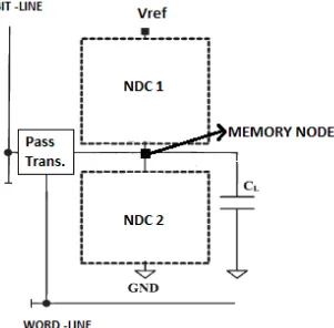
3.2 SRAM STRUCTURE USING NDC ELEMENTS
The general structure of static memory cell based on NDC elements is shown in
Fig. 3.7, where a pair of NDC elements is arranged in a latch configuration, and the
access to the cell is controlled by a pass transistor. The two load lines of NDCs produce
two stable points, as shown in Fig. 3.8 where the voltages at both points represent
different logic states. The logic ―0‖ is stored in the memory cell at the low voltage state
Fig. 3.7 Schematic Diagram for NDC based SET memory cell
When the word line is low i.e. cell not selected, the output of the memory node
shows one of two stable voltage levels, depending on the previously written bit-line level.
To write data in memory cell, data is placed on the bit line and the word line is raised.
The voltage of the memory node is then charged or discharged to a desired voltage level.
3.3 SET BASED READ/WRITE SWITCH
While single-electron memory can use a MOS transistor for read/write operation,
we designed SET based read /write switches to be used with the static memory since no
fabrication process is currently available for integrating MOSFET devices and SET-based
NDC elements [5]. Further SET circuits are not able to co-simulate with MOSFETs in the
Monte Carlo simulator SIMON. The Coulomb oscillation property of SETs is exploited
to perform read or write operation, as shown in Fig. 3.9.
(b)
Fig. 3.9. SET transistors for (a) WRITE and (b) READ.
The voltage Vgs at which the drain current becomes zero turns the switch OFF and the
voltage at which the current is maximum turns the switch ON. For the WRITE transistor
of Fig. 3.9 (a) where Vds = 400mV, Cd = Cs = 0.1aF, Rd = Rs = 0.1MΩ, Cg = 0.2aF, the
switch is on or off when Vgs = 600 mV or 200mV, respectively. When the switch is on,
the data is applied to the drain, and the corresponding voltage is written onto the memory
node. The parameters for READ transistor of Fig. 3.9 (b) are: Cd = Cs = 0.0667aF, Rd =
Rs = 0.1MΩ, Cg = 0.133aF, and CL = 6aF. The switch turns on or off when Vgs =
900mV or 260mV, respectively. When the switch is ON, the corresponding voltage is
sensed across the load capacitance CL.
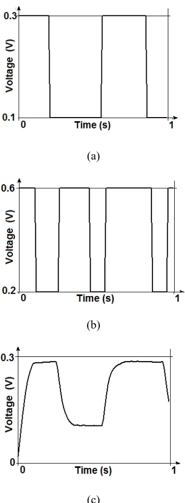
Fig. 3.10. shows the transient waveforms of the NDC based SET static memory cell for
WRITE operation. When the WRITE switch is OFF (i.e., the voltage is low in Fig.
3.10(b)), the output of the memory node shows that the storage node latches to one of two
(a)
(b)
(c)
Fig. 3.10. Memory write input and read output waveforms: (a) input data; (b) write
switch; (c) voltage on memory node.
When the WRITE switch is ON (i.e., the voltage is high in Fig. 3.10(b)), the data is
switching on the READ circuit, and the voltage stored at the memory node is measured
across the load capacitance CL.
3.4 PERFORMANCE METRICS FOR SRAM STRUCTURE
We discuss the different performance metrics for single electron tunnelling (SET)
based static memory cell design using unique negative differential conductance (NDC),
with emphasis on power optimization. While various NDC elements have been proposed
for memory cell design [3-6], they operate with different performance which includes the
peak-to-valley current ratio (PVCR), operating temperature, reliability and standby power
dissipation. For instance, the memory cell using an NDC element from [5] works at liquid
nitrogen temperature (77K) with standby power of 6.6nW and PVCR of 4.7. An ideal
memory cell using SET devices should work reliably at room temperature with a
reasonable PVCR and low power dissipation
a) Peak- to- Valley Current Ratio (PVCR):
A key figure of merit for negative differential conductance characteristic is the
ratio of the peak current to the valley current. The higher the value of PVCR, the better
the NDR device is for a variety of circuit applications.
b) Temperature
The smaller the capacitance of the islands C and the larger the quantum
confinement energy Ep, the larger is the Coulomb energy Ec and thus the larger is the
operation temperature T. To allow single electron device operation, the Coulomb energy
Ec must be the dominating energy in the system when compared to the thermal energy
capacitance decreases and the quantum confinement energy increase. A good single
electron device should work at room temperature (300 K), or at least at liquid nitrogen
temperature (77 K).
c) Maximum Power
Because of small capacitances and the low number of electrons involved in
charging and discharging, the power consumption of SET is usually orders of magnitudes
smaller than that of conventional memories. Power consumption in static memory design
depends on the drain voltage range of the NDC element. The smaller the voltage range
the smaller is the reference voltage Vref (see Fig 2). The standby power also depends
upon the current require to hold the two stable states(I ref)
Standby Power (W) = Vref * Iref
However there is a trade-off between low standby power consumption and reliability.
d) Reliability
The difference in voltage between the low voltage state (logic ‗0‘) and the high
voltage state (logic ‗1‘) is referred to as Logic margin. A higher value for logic margin
makes the system more reliable. The larger difference in the stable states prevents
incorrect logic errors caused due to external disturbances. Large logic margins results in
large standby power consumption and hence a good compromise between the two must
be obtained.
e) Background charge
This term denotes charged impurities located close to a quantum dot, as well as
parasitic capacitances of other quantum dots which induce charges and often destroy the
technologies which allow production of impurity free materials or materials where
impurities accumulate in regions where they do not disturb device behaviour.
f) Circuit Complexity
The number of elements used in the design. The fewer the elements the more
compact the design becomes and the more the memory density.
3.5 SRAM CELL BASED ON SINGLE ELECTRON NDC
ELEMENTS
3.4.1 SRAM CELL A
In the first SRAM cell, we use the NDC element from section 3.2.3 proposed by
Lee and Jeong. The schematic diagram for the SRAM cell is shown in Fig 3.11.
Table 3.1 Parameters for load and driving NDC Blocks
Ct Rt Rm Cg1 Cg2
NDC 1 0.1aF 1MΩ 1MΩ 0.54aF 0.54aF
Fig. 3.11 Schematic of SRAM cell using NDC element from Section 3.2.3.
The parameters for the load and driving NDC locks are stated in the Table 3.1 .The
corresponding load line diagram, Fig. 3.12 shows that any voltage V0 such that 0 < V0
< 250 applied to the memory node will eventually settle down at the low stable state, in
applied to the memory node will eventually settle down at the high stable state, in this
case 400m, representing the logic 1 .
Fig. 3.12 Load Line diagram for SRAM cell using NDC element from Section 3.2.3
Table 3.2 Logic state for different values of Input voltage Vds
Input voltage Vds
(mV)
Memory Node Voltage (mV) Logic
Switch ON Switch OFF
50 130 150
Logic 0
200 190 150
300 400 400
Logic1
400 400 400
Table 3.3.Performance metrics for SRAM Cell of Fig 3.11
Operating Temperature (K) No. of Elements Standby power (nW) Logic margin (mV) P.V.C.R Background charge dependent 77K
6 junctions +
4 capacitors
6.6 250 4.7 yes
The Table 3.2 and Fig 3.13 show the result of different input voltage Vds on memory
node using the Monte Carlo simulator SIMON. The Table 3.3 shows that the SRAM cell
3.4.2 SRAM CELL B
In the second SRAM cell, we use the NDC element from section 3.2.2 proposed
by Mahapatra and Ionescu. The schematic diagram for the SRAM cell is shown in Fig
3.14
Table 3.4 Parameters for load and driving NDC Blocks
Cj Rj Cg1 Cg2 Ibias CL
NDC 1 0.15aF 1MΩ 0.5aF 0.5aF 10nA 2aF
NDC 2 0.15aF 1MΩ 0.5aF 0.5aF 10nA 2aF
Table 3.5 Logic state for different values of Input voltage Vds
Switch Vds (mV) Memory Node Voltage (mV) Logic
Switch ON Switch OFF
50 100 110
Logic 0
100 110 110
300 250 230
Logic1
400 270 230
The parameters for the load and driving NDC locks are stated in the Table 3.4. Any
voltage V0 such that 0 < V0 < 250 applied to the memory node will eventually settle
down at the low stable state representing the logic 0 i.e. 110mV and any voltage V1 such
that 250 < V1 < 400 applied to the memory node will eventually settle down at the high
3.5 and Fig 3.15 show the result of different input voltage Vds on memory node using the
Monte Carlo simulator SIMON.
Fig. 3.15 Results from SIMON show that the two stable voltages are110mV and 230mV
The Table 3.6 shows that the SRAM cell has a standby power of 2.4 nW for a Vref of
300mV and a standby current of 7.9nA with a logic margin of 120 mV and a P.V.C.R of
Table 3.6.Performance metrics for SRAM Cell of Fig 3.14 Operating Temperature (K) No. of Elements Standby power (nW) Logic margin (mV) P.V.C.R Background charge dependent
50K 8 jns + 6 cap 2.4 120
approx.
6
yes
Table 3.7.Performance metrics for SRAM Cell of Fig 3.11
Design Operating Temperature (K) No. of Elements Standby power (nW) Logic margin (mV) P.V.C.R Background charge dependent SRAM cell 1 77K
6 jns + 4
cap
6.6 250 4.7 yes
SRAM
cell 2
50K
8 jns + 6
cap
2.4 120 approx. 6 yes
Table 3.7 compares the SRAM cell A from Section 3.4.1 and SRAM cell B from
Section 3.4.2in terms of performance metrics. Even though SRAM cell B has lower
standby power consumption, it is still not preferred over SRAM cell A since the
operating temperature is much lower than the latter. So we try to optimize the SRAM cell
CHAPTER IV
STANDBY POWER OPTIMISATION
TECHNIQUE FOR STATIC MEMORY CELL
As we have seen from earlier chapters that only a few SET elements having NDC
characteristic have been proposed. Further no discussion have been made on parameter
optimisation for low power memory application .The following chapter shows an
optimisation technique for standby power optimisation.
4.1 OPTIMISATION METHODOLOGY
For convenience of discussions, we use the NDC element from [5] as an example
(see Fig. 3.5) where the junction capacitance Cd = Cm = Cs = 0.1aF and junction
resistance Rd = Rm = Rs = 1MΩ. When the value of gate capacitance Cg is chosen
properly (anywhere between 0.4aF and 1.5aF), the negative differential conductance
(NDC) characteristic can be observed.
When pair of NDC elements are connected in a latch configuration with the
power supply of Vref, their NDC curves intersect at two stable points which represent
two different logic states (i.e. ―0‖ and ―1‖) as discussed in section 3.2. By adjusting the
reference voltage, each stable point can be designed to take place at the valley of the I–V
characteristics of each NDC element thereby reducing the current required to hold the
stable states. The results from the Monte Carlo simulation for current–voltage
increases, the voltage Vref needs to be reduced considerably for the two load lines of
NDC elements to intersect at two stable points.
Fig. 4.1. Standby power vs. gate capacitance for memory cell using NDCs of [5].
The current required to hold both logic states is also reduced as the gate
capacitance increases. Thus, the overall standby power goes down significantly with
increase in Cg. Fig. 4.2 shows the standby power consumption as a function of gate
capacitance.
The difference in voltage between the low voltage state (logic ‗0‘) and the high
voltage state (logic ‗1‘) is referred to as logic margin. A higher value for logic margin
makes the system more reliable. Fig. 4.3 shows the logic margin versus gate capacitance.
According to our simulations using Monte Carlo simulator SIMON [7], the logic margin
decreases slowly as the gate capacitance (Cg) increases, thereby gradually making the
system sensitive to noise fluctuations. Therefore, as the value of Cg increases (up to
a minimum of 0.59nW) at the cost of reduced logic margin. Fig. 4.4 plots the standby
power vs. logic margin of the cell. It can be seen from the figure that the standby power
increases to 1.54nW for a corresponding logic margin value of 180 mV (when Cg = 0.7aF
with power supply of 0.39V), beyond which the power increases considerably with only a
little improvement in reliability.
Fig. 4.2. Logic margin vs. gate capacitance for memory cell using NDCs of [5].
Thus, for the best trade-off between power and reliability, Cg was set to 0.7aF
with over 4x power improvement over the one of [5]. For the gate capacitance Cg=0.7aF
and reference voltage Vref of 0.39V, the two stable voltage levels stay approximately at
the values of 106 mV and 286 mV with the current of 3.94 nA.
4.2 EFFECT OF TEMPERATURE AND RANDOM BACKGROUND
CHARGE
As the temperature increases, the SET sub threshold slope decreases due to the
smearing of the Coulomb blockade. Consequently, the NDC characteristics get
deteriorated, resulting in an increase in the current required to hold the logic states, which
contributes to the increased standby power consumption.
Fig. 4.5 Logic margin vs. standby power at different background charges.
Fig. 4.5 demonstrates the effect of temperature on the standby power versus logic margin
curves. It can be seen that as the temperature increases, the standby power consumption
begins to shoot up at lower values of logic margin (corresponding to higher values of Cg).
Fig. 4.6 illustrates the effect of background charges on the standby power versus logic
margin curves. Similar to the temperature effect, the background charges also raise the
standby power consumption for a given logic margin.
The effects of temperature can be reduced by further reducing the capacitance
which is done by reducing the size of the island to below 10 nm. New material systems
which have lower dielectric permittivity or exhibit higher quantum confinement energy
due to their reduced effective mass may reduce this spatial restriction noticeable.
developed and studied. This takes a lot of time and research effort. Hence the economical
factor limits this possibility drastically. For reducing the effects of random background
charge we need to find process technologies which allow production of impurity free
materials or materials where impurities accumulate in regions where they are not
CHAPTER V
A NOVEL SET BASED ELEMENT WITH
MULTIPLE PEAK NDC
Traditional computer systems use binary logic for their operations. Representing
data in a MVL system is more effective than the binary-based representation because
MVL storage allows storing more bits of information per memory cell thereby increasing
its data processing capability per unit chip area. It also improves the efficiency of
arithmetic operations by reducing the number of operations required to implement
particular mathematical functions. The number of interconnections can be significantly
reduced, with major impact in all design parameters. Lesser area dedicated to
interconnections leads to more compact and shorter interconnections lowering the
interconnect switched capacitance, and hence lowering the global power dissipation.
Currently MV logic is used in some top EDA tools as mathematical technique to
minimize binary logic E.g. Synopsys, Cadence, Lattice. Many researchers expect that
new optical, DNA and quantum computers that will arrive before year 2020 will use MV
logic. An important part of this effort will be the development of MVL Nano scale
memory systems that can store the ternary (base 3) or quaternary (base 4) numbers that
will be used by MVL arithmetic circuits. In this chapter we introduce a new SET
architecture exhibiting multiple NDC peaks in the VI characteristic. Further its
5.1 MULTIPLE PEAK NDC ARCHITECTURE
Fig. 5.1. Proposed multiple peak Set based NDC architecture
Our proposed system consists of four islands, positioned as depicted in Fig. 5.1, between
the source and the drain electrodes. The islands 1 and 3 form two single electron
transistors, SET 1 and SET 2, allowing a current to flow between voltage source and
ground through the island 4, which acts as a single electron box (SEB). The capacitors Cg
and Co are capacitances coupled with islands and Cd, Ca, Cm, Cb and Cs are the
capacitances of tunnel junctions. Considering all tunnel junction capacitance of the four
island array to be equal to Ct, multiple NDC peaks are observed when Cg/Ct=2 and
Co=2Cg. Here two additional Coulomb Blockade (CB) gaps are seen in the interval of
[V2, V3] and [V4, V5] called the secondary coulomb blockade SCB 1 and SCB 2, in
addition to the primary CB gap at [0, V1]. The origin of the additional gaps is attributed
to the formation of the stationary charge configurations (SCC) which traps electrons
thereby blocking the flow of electric current resulting in the negative differential slope.
According to the orthodox theory, the tunneling rate across the tunnel junction is
(1)
Where e is the electronic charge, Rj is the tunnel resistance of the jth junction, T is the
temperature, and ∆F is the change in the free energy of the system when an electron has
tunneled through the tunnel junction with the tunneling resistance Rj with the electron
configuration change from {n} to {n‘}, where {n} is the charge configuration on islands.
A SCC is a local minimum of the free energy in the configuration space. That is, the free
energy change ∆F, due to the transition from the SCC to its adjacent configuration, is
greater than zero making the tunneling process energetically unfavorable so that the
electrons get trapped and consequently the SCB 1 is established.
5.2 MECHANISM FOR MULTIPLE NDC PEAKS
Fig. 5.2 I–V characteristics for the multiple peak SET block and comparisons of tunnel
The mechanism for NDC in this device structure is shown in Fig. 5.2 and can be
described as follows. At low drain voltage (Vd), where Vd is less than V1, the entrance
of the electron or hole through each side tunnel junction is restricted due to Coulomb
blockade effects. In this case, the electron configuration of islands is {0, 0, 0, 0}. As Vd
is increased above V1, a single hole enters through the drain tunnel junction onto the ‗
island 1‘ causing the tunneling process {0,0,0,0}→{1,0,0,0}→{0,1,0,0} almost instantly
due to high electron hopping rate at junction 2. The stationary configuration SCB1
corresponding to (1, 1,-1,-1} is reached eventually. The process which leads to the
break-up of SCB1 is achieved by introduces another hole into the array giving rise to the
charge configuration (2, 1,-1,-1) which is the offset to the formation of the stationary
configuration SCB2 corresponding to {1, 2,-1,-1}. The SCB 2 persists in the voltage
interval V4< Vd< V5. If the electron configuration changes from to, where is the charge
configuration on islands then each tunneling process with increasing voltage is as
follows.
A: nA = { 0,0,0,0 } nA‘ = {1,0,0,0}
B: nB = { 1,0,0,0} nB‘ = {0,1,0,0}
C: nC = { 0,1,0,0 } nC‘ = {0,1,0,-1}
D: nD = {0,1,0,-1 } nD‘ = {0,1,-1,0}
E: nE = {0,1,-1,0 } nE‘ = {1,1,-1,0}
F: nF = {1,1,-1,0 } nF‘ = {1,1,-1,-1}
G: nG = {1,1,-1,-1} nG‘ = {2,1,-1,-1}
Fig. 5.3 Probable electron charge configuration
Fig 5.3 shows the probable electron charge configurations. The configurations nB ,nD
,nE, nF,nH are reached by very fast tunneling processes which take place almost
simultaneously and hence are not visible in the figure.
5.3 EFFECT OF TEMPERATURE AND BACKGROUND
CHARGE
The results of the Monte Carlo simulations for current–voltage characteristics for
several values of temperatures are shown in Fig. 5.4.
Fig. 5.5 Effect on Random background charge on the multiple peak NDC
We see that the peak-to-valley current ratio in the NDC characteristics is reduced
as temperature increases. This is due to the smearing of the SC blockade at high
temperature. Fig 5.5 shows the effect of background charge on V-I characteristics. As we
see the design is sensitive to background charge. Most SETs suffer from major stability
problems which are common to other candidates such as nanowire transistors, nanotube
(CNT), RTD, NEMS and molecular devices since their smaller dimensions increase
sensitivity to fluctuation such as higher temperature and random background charge.
5.4 A NOVEL MVL SRAM CELL BASED ON SINGLE
ELECTRON DEVICES
The schematic diagram of the multiple peak SET static memory cell is shown in Fig. 5.6
, which is similar to the resonant tunneling diode (RTD)/heterojunction field-effect
transistor (HFET) static memory cell [19]. However, the significant change in this circuit
is the replacement of the vertical RTD with the SET-based NDC block, which use the
single electron charging effect. Our static memory cell consists of a pair of SET blocks in
have set the background charge to be zero, assuming that a suitable fabrication process
could control the background charge.
One-bit data is stored in the latch, which is constructed from a pair of the SET
blocks of which parameters are optimized for proper memory operations. The set of
parameters used in Fig. 5.6 is summarized in Table 5.1(a) and (b). The voltage of the SET
block latch was biased at 1 V. Fig. 5.7 shows the load-line diagram with three stable
points at temperature T=0K. The logic ―0‖ is stored in the memory cell at the first low
voltage state, logic ―1‖ is stored in the memory cell at the second low voltage state and
the logic ―2‖ is stored at the high voltage state.
Table 5.1. (a) Parameters for the multiple peak static memory cell (b) Parameters for
write switch
(a)
SET Block Ct (aF) Rt (MΩ) Cg (aF) Co (aF)
NDC 1 0.2 0.1 0.4 0.8
NDC 2 0.2 0.1 0.4 0.8
(b)
Cd Rd Cs Rs Cgs Vgs(mV)
(aF) (MΩ) (aF) (MΩ) (aF) ON OFF
0.1 0.1 0.1 0.1 0.2 600 200
By adjusting the supply voltage, each stable point can be designed to take place at the
valley of the I–V characteristics of each SET block. The current required to hold the state
three stable voltage levels exist approximately at 0.3V, 0.5 V and 0.7V with the current
of 15nA, 124nA and 16.5nA respectively.
Fig. 5.7. Load line diagram for memory cell using two peak NDC element for Ct =0.2
with ratio Cg/Ct=2 at T=0K.
Fig. 5.8 shows the transient waveforms of the multiple peak SET static memory cell of
Fig. 5.6. When the cell is not selected (switch OFF), the output of the memory node
shows that the storage node latches to one of three stable voltage levels (0.3, 0.5 or 0.7),
depending on the previously written input. Here 0.1V corresponds to logic 0, 0.7V
corresponds to Logic 1 and 1.1 corresponds to logic 2 respectively at the input line. To
write data in memory cell, corresponding voltage is placed on the input line and the write
switch is turned ON. When the switch is turned off the voltage at the memory node,
settles down at stable voltage level l and the stable state is maintained with the average
standby power of 52nW with an average logic margin of 197 mV approximately.
Therefore, the multiple peak SET static memory element needs to be optimized for low
Fig.5.8 Memory write input and read output waveforms: (a) input data; (b) write switch;
5.5 STANDBY POWER OPTIMISATION OF MVL SRAM
CELL
The Fig 5.9 shows the standby power consumption vs. logic margin for different
values of Ct at temp 0K for the ratio Cg/Ct =2. As the value of Ct is reduced from 1aF to
0.1aF the standby power consumption increases drastically along with an increase in
logic margin. We also see in Fig 5.10 that for a fixed value of Ct (say 0.2) and Cg/Ct=2,
the increase in temperature further compromises the standby power consumption
drastically. This is due to the fact that an increase in temperature raises the valley current
thereby reducing the PVCR. By Monte Carlo method of simulation we find that for
improving the power consumption at temperatures up to 77 K the ratio of Cg/Ct must be
equal to 3.
Fig.5.9 Standby power vs. Logic margin at different values of Ct for the ratio Cg/Ct
Fig.5.10 Standby power vs. temperature at Ct=0.2aF for Cg/Ct=2
Fig. 5.11. Standby power vs. Logic margin at different values of Ct for the ratio Cg/Ct
=3 at T=77K.
Fig. 5.11 show the power consumption vs. logic margin at different values of Ct for the
ratio Cg/Ct =3 at 77 K. We see that at temperature 77 K, as the value of Ct decreases the
because as the island size is reduced i.e. Ct is reduced; the device can operate at higher
temperature. Therefore at temperature 77 K, we optimize our parameter using the ratio
Cg/Ct =3 and Co=2Cg. The parameters for the NDC blocks of Fig.5.4(a) are Ct =0.1aF,
Cg = 0.3aF, Co= 0.6aF.
Fig. 5.12. Load line diagram for memory cell using two peak NDC element for Ct =
0.1aF with ratio Cg/Ct=3 at T=77K.
The Fig 5.12 shows the load line diagram for the optimized MVL SRAM design. For
Vref of 1.41V the stable voltages are at 437mV for logic ‗0‘, 707 mV for ‗logic ‗1‘and
979 mV for logic ‗2‘ respectively with an average logic margin of 270 mV. The average
current required to hold the three states is 6.99E-10 resulting in an average standby power
5.6 A NOVEL QUATERNARY SRAM CELL
The parameters of the NDC architecture of Fig.5.1 can also be optimized to have
three NDC peaks in the V-I characteristics as shown in Fig 5.13. This three peak NDC
block can used to build a quaternary memory cell with four stable states as shown in Fig.
5.6.
Fig. 5.13. IV characteristic for three peak NDC element used in Quaternary memory cell
.
Table 5.2. Parameters for the Quaternary memory NDC elements
SET Block Ct (aF) Rt (MΩ) Rd(MΩ) Cg (aF) Co (aF)
NDC 1 0.1 0.1 1 0.3 1.3
Fig.5.14. Load-lines for load and driving SET blocks for the Quaternary memory
cell
The parameters for both NDC blocks for obtaining three peaks are given in the Table 5.2
considering Ct =Cd=Ca=Cm=Cb=Cs and Rt= Ra=Rm=Rb=Rs. The Fig. 5.14 shows load
line diagram for the loading and driving SET blocks of the memory cell at T=77K..The
four stable voltages representing Logics 0,1,2,3 are at 0.48V, 0.63V, 0.82V and 0.97V
respectively with an average standby current of 3.5nA. The quaternary memory cell
CHAPTER VI
RESULTS AND DISCUSSIONS
The comparisons of our proposed two peak SET static memory cell and our three
peak NDC based SET static memory cell with available SET SRAM cells are
summarized in Table 6.1. The SET/MOSFET proposed in [5], can store only binary
values with a large standby current of 10nA and a Vref of 5.5V. The memory cell thereby
consumes a standby power of 5.5nW with a logic margin of 250mV. With further standby
power optimization in section 4.1, the best trade-off between power and reliability was
obtained by setting the value of gate capacitance to 0.7aF.
Table 6.1 Comparison of SET based SRAM cell
Design
SET/MOSFET Proposed
2 peak Proposed 3 peak [5] Operating Temperature(K)
77 77 77
Avg. Standby
Power (nW)
5.5 0.98 5.06
Logic states 0,1 0,1,2 0,1,2,3
No of elements 6 jns+ 4 cap 10 jns + 6 cap 10 jns + 6 cap
Avg. Logic Level
difference (mV)
For a reference voltage Vref of 0.39V, the two stable voltage levels stay
approximately at the values of 106 mV and 286 mV with the current of 3.94 nA.
However this memory cell could still had only two stable states enabling is use only in
binary memory cell. Our proposed ternary memory cell performs better at the same
operating temperature of 77K. Due to its two peak NDC characteristic it allows an
additional stable state making it suitable in the design of ternary memory. This makes the
memory more compact by reducing the interconnections. A reduction in the inter-connect
switched capacitance also lowers the global power dissipation.
Table 6.2 Comparison of different SRAM cell
Design SET/ MOSFET [5] Our Proposed 2 peak Our Proposed 3 peak RTD/ HFET [19] CMOS SRAM [20]
No of elements
1 Tr +2 SET
based NDC
1 Tr +2 SET
based NDC
1 Tr +2
SET based
NDC
1Tr +2
RTD
6 Tr
No of Logic
states
2 3 4 2 2
Background
Charge
Dependent
YES YES YES NO NO
Standby Power
(W)
The ternary memory can therefore store three logic states 0, 1 and 2 at a standby current
of 6.99E-10 resulting in an average standby power consumption of 0.98nW. The Vref of
1.41V gives stable voltages at 437mV, 707mV and 979mV respectively with an average
logic margin of 270 mV. Thus it provides more storage with a significant reduction in
standby power and higher logic margin. Our proposed 3 peak architecture consumes a
standby power consumption which is comparable to the SET/MOSFET in [5] but has an
advantage of 4 logic states making it suitable for use in Quaternary storage with around
the same power consumption and slightly lower logic margin.
Table 6.2 compares the SRAM cell of different technologies. Our multiple valued
logic SET memory designs provide lower standby power than the SET/MOSFET from
[5] as well as RTD/HFET. Although the static memory cell could not compete with the
CMOS static memory cell, which consumes less than 1 pW [14], it is suitable for the
high-density memory system because of its more compact size than the CMOS static