Progression towards high efficiency
perovskite solar cells via optimisation of
the front electrode and blocking layer
Yates, HM, Afzaal, M, Walter, A, Hodgkinson, JL, Moon, SJ, Sacchetto, D,
Brauninger, M, Niesen, B, Nicolay, S, McCarthy, M, Pemble, ME, Povey, IM and
Ballif, C
http://dx.doi.org/10.1039/C6TC04647A
Title
Progression towards high efficiency perovskite solar cells via optimisation
of the front electrode and blocking layer
Authors
Yates, HM, Afzaal, M, Walter, A, Hodgkinson, JL, Moon, SJ, Sacchetto,
D, Brauninger, M, Niesen, B, Nicolay, S, McCarthy, M, Pemble, ME,
Povey, IM and Ballif, C
Type
Article
URL
This version is available at: http://usir.salford.ac.uk/40980/
Published Date
2016
USIR is a digital collection of the research output of the University of Salford. Where copyright
permits, full text material held in the repository is made freely available online and can be read,
downloaded and copied for noncommercial private study or research purposes. Please check the
manuscript for any further copyright restrictions.
For more information, including our policy and submission procedure, please
Journal Name
ARTICLE
Received 00th January 20xx, Accepted 00th January 20xx DOI: 10.1039/x0xx00000x
www.rsc.org/
Progression towards high efficiency perovskite solar cells via
optimisation of the front electrode and blocking layer
Heather M Yates,*a Mohammad Afzaal,a Arnaud Walter,b John L Hodgkinson,a Soo-Jin Moon,b Davide Sacchetto,b Matthias Bräuninger,c Björn Niesen,cSylvain Nicolay,b Melissa McCarthy,d Martyn E Pemble,d Ian M. Povey,d and Christophe Ballifb
The effects of fluorine doped tin oxide (FTO) electrode, titanium dioxide (TiO2-x) blocking layer (BL) and perovskite (methyl ammonium lead triiodide) preparation on the overall properties of the photovoltaic cells have been studied. The FTO electrode was deposited by atmospheric pressure chemical vapour deposition (APCVD) and the hole blocking layer by spin coating, atomic layer deposition (ALD) or sputtering. We have shown the importance of obtaining uniform thin films of FTO, with low sheet resistance to aid the formation of pin hole free uniform TiO2-x blocking layers and hence well adhered, perovskite layers. Optimal BL thickness was 20 nm, while thicker films gave decreased shunt resistance and a greater number of pin holes through the layers. We also showed that the conformal nature of ALD and magnetron sputtering, along with their increased uniformity control over spin coating again improved cell efficiency. The main improvement comes for the smaller Roc, attributed to an improved electrical transport through particularly the sputtered TiO2-x blocking layer. After identifying the optimised parameters, all the properties were combined to fabricate large solar cells (1 cm2) yielding power conversion efficiencies beyond 16%.
Introduction
In recent years there has been an intensification of interest over solid-state organic-inorganic hybrid perovskite solar cells. Early work starting with Mitzi et al1 with tin based iodides, then
continuing with progressive changes from tin to lead halides2
and liquid to solid electrolytes in particularly that of spiro-OMeTAD3,4 which dramatically improved cell efficiency from
around 3.8% to 9.7-10.9%. In addition there have been changes to the type/or mix of halides,5,6 organic cation7 and more
recently use of ‘triple cations’ with the addition of cesium to increase the durability of the films during cell processing.8
These gradual changes have led to present day efficiencies in excess of 22%.9
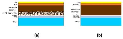
The basic and most common types of cell are the mesoscopic and planar structures, which are illustrated schematically in figure 1. In the mesoscopic form the metal halide perovskite absorber is infiltrated through a charge-conducting mesoporous scaffold, often TiO2 (titanium dioxide).
The photogenerated electrons from the perovskite layer are
[image:2.595.308.548.572.648.2]transferred to the mesoporous sensitized layer through which they are transported to the electrode and extracted into the circuit. This active layer is contacted with an n-type material for electron extraction (Electron Transport Layer - ETL) and a p-type material for hole extraction (Hole Transport Layer - HTL). The ETL layer also acts as a blocking layer (BL) to block recombination between the electrons in the front electrode and the holes in the perovskite. In contrast the planar structure does not have a scaffold so after light absorption both charge generation as well as charge extraction occurs in the perovskite layer. Both types of carriers are transported through the perovskite to their respective contacts. Usually a transparent conducting oxide (TCO) often F-doped tin oxide or indium tin oxide is used for the front electrode contact and gold for the back contact.
Fig. 1 Schematics of a perovskite based cell (a) mesoscopic, (b) planar.
The majority of literature published on this subject concentrates on the perovskite layer itself, with studies on its deposition,10-12 composition, structure,13 and the stability14 and
how it effects the cell characteristics.15,16 However, there is
much less discussion on the effects of other layers such as the BL (ETL) and TCO electrode. As already stated the BL acts to
a.Materials and Physics Research Centre, Cockcroft Building, University of Salford,
Manchester, M5 4WT, United Kingdom. E-mail: [email protected]
b.Centre Suisse d’Electronique et de Microtechnique (CSEM), PV-Center,
Jaquet-Droz 1, 2002 Neuchâtel, Switzerland
c.Ecole Polytechnique Fédérale de Lausanne (EPFL), Institute of Microengineering
(IMT), Photovoltaics and Thin-Film Electronics Laboratory, Rue de la Maladière 71b, 2002 Neuchâtel, Switzerland
d.Tyndall National Institute, Cork, Ireland
ARTICLE Journal Name
block recombination between the TCO electrons and the perovskite holes, while at the same time needs to provide efficient electron extraction from the perovskite to TCO. A thicker BL would decrease the charge recombination between the perovskite holes and TCO electrons, but would also reduce the electron flow to the TCO due to a higher series resistance in the cell, so a balance of conditions is required. A detailed studied by Choi et al17 looked at the deposition method and
resulting properties of BLs for producing planar solar cells emphasizing the importance of well-defined, defect free morphologies with uniform thickness. Most cells reported use TiO2, although alternatives materials have been tested such as
SnO2,18 composite graphene/TiO219 and ZnO.20
The role of the TCO characteristics has had very limited discussion, with commonly researchers using a commercially supplied standard material. The most utilised TCO is F-doped SnO2 (FTO) such as TEC 7, TEC 8 (NSG), or TCO22-15 (Solaronix).
Previous work by us21 concentrated on FTO’s optimised for use
in thin film silicon (Si) PV cells, which required high optical transparency, low resistivity and high surface roughness. The latter to increase internal light trapping to improve the efficiency of light use by the absorbing layers as Si (especially a-Si) has a low absorption efficiency. For perovskite cells the first two properties still apply, but as perovskite already has excellent absorption coefficients22 the overriding factor is to
achieve a suitable uniform surface to enable good adhesion and no pin holes through the BL and hence direct perovskite contact. The FTO morphology directs that of the BL and hence that of the perovskite so is an important factor towards cell efficiency. A too rough a surface tends to lead to FTO spikes or pin holes into the perovskite and hence fast electron/hole recombination. A non-uniform, rough surface also can lead to lower adhesion between the various layers, with the knock-on effect of poorer films and much lower cell efficiencies. Another important and related factor is the wettability of the TiO2-x
surface to the perovskite precursor solution and hence its solid surface coverage and crystallinity. It has previously been shown that use of a rougher TiO2-x surface gave better wettability, and
thereby a lower energy barrier to the heterogeneous nucleation on the liquid/solid interface.23 The perovskite layer
improvement (coverage, adhesion and crystallinity) in turn led to improved cell properties. Hence, there is an advantage in starting with a relatively rough TCO surface which can lead to the formation of a similar morphology for the BL.
In this paper, we concentrate on studying the effects of the FTO electrode and TiO2-x blocking layer. In addition some
changes to the perovskite precursor composition were considered on the overall properties of the PV cell. From this we aim to combine the optimised properties leading to improved cell efficiencies. For the FTO films the effects of roughness, dopant level and resistivity on the cell characteristics will be discussed. We show that the combination of FTO properties required to give low resistivity, high optical transmission and relatively uniform surfaces will aid improvement of PV efficiency.
For the BL, the effects of different deposition methods, namely those of Atomic Layer Deposition (ALD), spin and
sputter coating will be studied to show the importance of technique chosen, layer thickness and the need to produce dense, pin hole free conformal films. In addition, optimisation of the spin coated perovskite via precursor/solvent changes will be studied.
Experimental
Thin films
Fluorine doped tin oxide
Thin films were deposited by APCVD at deposition temperature of 600 °C using monobutyl tin trichloride (MBTC) with 0.2, 0.6 or 1.0 M aqueous trifluoroacetic acid (TFAA), delivered with a Sn precursor to H2O molar ratio of [1]:[5] or [1]:[30]. Precursors
were vapourised using either bubbler (MBTC at 125 °C, 0.7 L min−1 carrier gas) or flash evaporation (TFAA/water mix, 0.6 L
min−1 carrier gas). N2 was used as the carrier gas. Process flow
was set to 7 L min−1 with oxygen (1.5 L min−1) giving a total flow
of ~ 9.8 L min−1. Deposition was on 1 mm thick borosilicate
(Corning Eagle 2000) glass. The heated substrate is translated, on an automated stage, beneath a static, non-contact CVD head (i.e. gas distributor) in an extracted, open atmosphere, enclosure. This allows the deposition of extended area films with high uniformity over 100 mm width (±2 %) and the length only limited by the translation table size. For these experiments samples of 100 mm x 100 mm were provided for cell fabrication. Film thickness was varied by changing the number of passes under the coating head. For each type of deposition parameter several samples were prepared. This then enabled the fabrication of a greater number of cells and hence increased confidence in the resulting data.
Titania blocking layers
Spin coated blocking layers were prepared by using a precursor solution, 0.15 M titanium diisopropoxide dis(acetylacetonate) Aldrich, 75 wt.% in isopropanol) in 1-butanol (Sigma-Aldrich, 99.8%). The precursor solution was spin-coated on a FTO glass substrate at 1000 rpm for 10 sec and 2000 rpm for 20 sec, which was followed by sintering at 450 °C for 30 minutes.
Thin-films of TiO2-x with 23 nm thickness have been
deposited by RF sputtering at 60 °C. The stoichiometry of the thin films could be controlled by adjusting the Ar and Ar:O2
flows in the sputtering chamber. Thus the electrical conductivity and the transparency of the TiO2-x films could be tuned in order
to get the optimal optoelectronic properties for the solar cells. Thin films with a range of thickness (10 nm - 30 nm) have been deposited employing a Cambridge Nanotech–Ultratech F200 ALD system. Tetrakis dimethylamino titanium (TDMAT) and H2O in an argon carrier flow were employed as the metal
precursor and oxygen source, respectively. The deposition temperature was 200 °C, leading to a deposition rate of 0.5Å/cycle.
Cell Fabrication
paste (Dyesol 18NRT) diluted in isopropanol (1 g in 10 ml) at 2000 rpm for 30 sec and annealed at 500 °C for 30 minutes. Three different perovskite recipes were used for the optimization of the perovskite layer. The same CH3NH3PbI3
precursor solution was used for recipes 1 and 2 but the dripping amount of toluene was increased from 60 µl to 1ml in recipe 2. 1.2M PbI2 (TCI) and CH3NH3I (Dyesol) were dissolved in a
mixture of ɣ-butyrolactone (GBL) and dimethyl sulfoxide (DMSO) (7:3 volume ratios) at 70 °C. A CH3NH3PbI3 precursor
solution was then spin coated on m-TiO2 substrate at 1000 rpm
and 5000 rpm for 10 sec and 30 sec, respectively. During the 2nd step of spin coating toluene was dropped on the substrate and perovskite layer was dried at 100 °C for 10 min. In recipe 3, 461 mg of PbI2, 159 mg of CH3NH3I, and 78 mg of DMSO (molar
ratio 1:1:1) were mixed in 600 mg of dimethylformamide (DMF) solution at room temperature with stirring for 1 h in order to prepare the CH3NH3PbI3 precursor solution. The precursor
solution was spin coated on m-TiO2 substrate in a two-stage
sequence (1000rpm for 10s followed by 5000rpm for 45s) and 0.75 ml of diethyl ether were dripped on the substrate 12 s before the end of the procedure. The substrate was then heated at 50 °C for 2 min and 100 °C for 10 minutes.24 Spiro-OMeTAD
solution was prepared by dissolving 72.3 mg spiro-OMeTAD (Merck), 28.8 µl 4-tert-butylpyridine (Sigma-Aldrich), 17.5 µl of a stock solution of 520 mg ml-1 lithium
bis(trifluoromethylsulfonyl)imide (Sigma-Aldrich) in 1 ml chlorobenzene and spin coated on top of perovskite layer at 4000 rpm for 30 seconds. The cells were then finished with the evaporation of a 100nm thick gold electrode.
Characterisation
Thin Films
The morphology and surface roughness of the samples were obtained by atomic force microscopy (NanoScope IIIa, Digital Inst. Ltd.). Images were also obtained via scanning electron microscopy (Philips ESEM FEG XL30). Film thickness for the FTOs was determined by etching the films with HCl/Zn metal to give a step edge, followed by surface profiling on a Dektak 3ST. The resistivity of the films was measured using a Jandel Universal four point probe. Hall effect measurements were performed on the TCO films to determine the carrier concentration and the electron mobility with a lab built system using an electromagnetic with a pole separation of 12.5 mm and current of 1.1 A to give a magnetic flux density of 0.66 T. A lab built spectrometer consisting of a 75 W xenon lamp and four broadband filters centring on four wavelengths (800, 650, 531, and 450 nm) was used to measure optical properties. A silica sample was used to calibrate the throughput of the integrating sphere. For more detailed optical measurements spectrophotometry (UV-Vis-NIR) was performed with a Perkin-Elmer Lambda 900 spectrophotometer equipped with an integrating sphere. Dark conductivity measurements of the TiO2-x samples were performed under 1mbar N2 atmosphere
and in the dark. During the measurement, the temperature is ramped up from room temperature to 180°C with a rate of 10 °C/min then the sample is slowly cooled down at a rate of 1
°C/min. The conductivity was taken during the cool down phase for a more precise temperature measurement.
Cell characterisation
All cells were characterized under a two-lamp class AAA WACOM sun simulator with an AM1.5g irradiance spectrum at 1000 W/m2. The cell area was defined using a metal mask. The
I-V characteristics of the cells were obtained under both reverse (from VOC to JSC) and forward (from JSC to VOC) bias. A Maximum
Power Point (MPP) tracking was usually performed to extract the stabilized power output. External Quantum Efficiency (EQE) spectra were acquired on a custom-made spectral response setup equipped with a xenon lamp, a grating monochromator and lock-in amplifiers.
Results and discussion
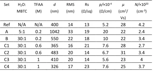
Thin films of SnO2:F were deposited by APCVD as previously
described by us25 with changes to F dopant level, tin precursor
to H2O molar ratio and thickness via the number of coater head
passes (Table 1).
d: Average film thickness, AFM – root mean squared (RMS) roughness, Rs: Sheet
resistance, p: resistivity, µ: mobility, N: carrier concentration
Initial trials with FTO sets A, B and C
For preliminary work two types of FTO were deposited with differing surface roughness (RMS 33nm, 22 nm), although of similar sheet resistance (~ 20 Ohm/sq). The reduction in roughness while keeping resistance constant was achieved by reducing film thickness and increasing the H2O:MBTC precursor
ratio. In APCVD (assuming only time of deposition is changed) it is expected that the film gets rougher as the film thickness increases. The FTO growth is columnar26 and polycrystalline27.
As different crystallographic orientations grow at a different rate the differences are accentuated as the film gets thicker, so increasing surface roughness. A thinner sample would exhibit increased sheet resistance, unless the dopant levels were increased to reduce bulk resistivity which may risk performance loss due to increased free carrier absorption. The first batch of samples (Set A) sent for the solar cell fabrication were produced using a 5:1 H2O:MBTC precursor ratio which had an thickness of
1042 nm. In contrast, the second batch of samples (Set B) produced using a 30:1 H2O:MBTC ratio had a thickness of 550
[image:4.595.303.554.343.460.2]nm. A third sample was deposited at the higher H2O:MBTC Table 1 Deposition conditions and electrical properties for FTO sets A, B and C. Set H2O:
MBTC TFAA
(M)
d
(nm) RMS (nm)
Rs (Ω/sq)
p/×10-4
(Ω/cm)
µ
(cm2/
Vs)
N/×1020
(cm-3) Ref N/A N/A 400 14 13 5.2 28 4.2
A 5:1 0.2 1042 33 19 20 22 2.4 B 30:1 0.2 550 22 18 10 22 3.4 C1 30:1 0.6 365 16 21 7.6 28 2.7 C2 30:1 0.6 483 20 14 6.7 31 3.4
C3 30:1 1 410 20 14 5.6 23 4
ARTICLE Journal Name
precursor ratio, but of similar thickness to Set A. This had a similar roughness to Set A but much lower sheet resistance. For the three FTO films discussed in this section it can be seen that if only the film thickness is increased (H20:MBTC fixed), then
roughness increases. However, if only the precursor ratio is increased (thickness fixed), then the roughness does not change. Therefore the roughness of the film depends on the film thickness not the precursor ratio. However, at the higher ratio the slightly increased doping level (as the TFAA is transported with the water) kept the resistance down. To put our results into perspective the samples were compared to a high quality commercially available FTO thin film – Solaronix TCO22-15. This has a 400 nm thick FTO layer with an Rms roughness of 14 nm. The electrical properties, as measured on our instrumentation, gave sheet resistance of 13 Ω/sq, carrier concentration 4.2 × 1020 cm−3 and mobility 28 cm2 V−1s−1. This was both thinner, with much lower roughness than our APCVD FTO, with lower sheet resistance and higher mobility. The electrical properties of this commercial product are in line with its much higher carrier concentration. Optical scattering (haze) measurements confirmed the variation in sample roughness showing an increase in haze with surface roughness. Reference cells were fabricated on the commercial FTO concurrent to production of those on our TCO samples. This is particularly important as it reduces the possibilities of small variations due to deposition equipment and/or operators.
Perovskite PV cells were fabricated on APCVD and commercial FTO with spin coated TiO2-x blocking layers,
followed (as described in experimental section) by a mesoporous TiO2 scaffold, perovskite, spiro-OMeTAD and Au
contact. Interestingly, both sets of FTO CVD derived cells performed well, exceeding the efficiency achieved with use of the commercial TCO, used as a reference, by over 1% abs. in each case (Table 2), representing an improvement in the order of 10%. This is particularly noticeable as the commercial TCO reference despite the lower sheet resistance and higher carrier mobility, which would be expected to give the cell a higher efficiency in removing the generated current, does not perform as well overall. However, it does have higher carrier mobility. This will decrease the optical transmission via free carrier absorption and hence reduce the amount of light reaching the absorber parts of the cell. The relationship between carrier concentration and transmission has been seen previously for TCO ZnO electrodes in thin film silicon solar cells28. In addition
the reference cell has a lower short circuit current density (Jsc),
which in previous cell literature has been related to lower internal light scattering due to the TCO increased smoothness25,29. The higher PCE values for Set A and B cells
[image:5.595.64.529.410.747.2]suggested that while using mesoporous scaffold layer FTO roughness at this level is not an issue. Previously it has been shown that addition of a scaffold layer tends to reduce series
Table 2 Cell data for set A, B and C.
Sample ID Method of blocking layer (nm)
PCE (%) Voc (mV) Jsc (mA/cm2) FF (%) Rsc ( Ω.cm2) Roc (Ω.cm2)
O ri gi na l r ec ipe ( Se t A an d B )
Reference spin coated 8.436 887 16.06 59.2 925 7.67
A1 Spin coated 9.858 911.8 17.4 62.12 1924 7.711
ALD (10) 10.06 921.6 18.38 59.42 6662 9.943
ALD (20) 10.37 946.5 18.44 59.4 3604 11.83
ALD (30) 6.156 858.7 17.64 40.65 695.2 29.74
B1 spin coated (10-15) 9.776 878.3 17.58 63.31 786.1 7.139
N ew r ec ipe (bs et A an d B
) Reference spin coated 13.35 1040 19.92 64.43 1175 3.783
A2 spin coated 13.37 1023 18.96 68.9 1043 5.473
spin coated 14.68 1029 20.29 70.34 1672 5.464
B2 spin coated 9.276 786.9 20.4 57.78 2786 8.112
N ew r ec ipe ( Se t C)
Reference ALD 15 1036 18.81 76.98 2874 5.441
Reference ALD 14.84 1043 19.19 74.18 2860 5.729
C1 ALD 4.569 761 18.71 32.09 72.07 17.39
C2 ALD 14.33 1043 19.27 71.33 1826 4.282
ALD 14.68 1047 19.86 70.58 2203 5.153
C3 ALD 14.7 1057 19.77 70.34 1640 4.614
ALD 11.34 10.2 19.4 56.61 447.7 8.169
C4 ALD 13.29 1075 19.5 63.4 898.7 7.076
ALD 14.66 1049 19.37 72.14 3330 7.565
N ew r ec ipe ( Se t C; re -m eas ur ed af te r 3 d ay s)
Reference ALD 15.18 1028 20.2 73.09 2106 5.015
Reference ALD 14.62 1023 20.35 70.18 2550 4.915
C2 ALD 15.4 1031 20.54 72.69 1830 4.927
C3 ALD 15.2 1049 20.25 71.67 4049 6.088
resistance (Roc) and hence increase fill factor (FF), along with the
open circuit voltage (Voc) and shunt resistance (Rsc).7
Choose of BL deposition method – spin coating vs ALD
This encouraging result prompted studies on the choice of method adopted for depositing the blocking layers. Use of ALD to accurately deposit BL at a range of thicknesses (10, 20 and 30 nm) established an optimum thickness of 20 nm, giving a further increase in PV efficiency as shown in Table 2. Too thick a coating gave a reduction in Rsc. A comparison of method used to deposit
the BL showed an advantage in using ALD opposed to spin coating with better Voc and hence device efficiency. This
improvement relates to the increased film density, conformal behaviour and better control of thickness uniformity, which for the spin coated samples was between 10 nm and 15 nm. ALD is a surface controlled, chemically self-limiting technique for depositing thin films. It is well documented for its ability to produce conformal and pin hole free layers with high thickness uniformity30. Using the same ALD process as us Chen et al31
demonstrated pinhole free, conformal deposition of only 2 nm TiO2 over Si layers. Other studies32 on the effect of the BL
deposition method, this time ALD, spray pyrolysis and sol-gel also concluded that the improved cell efficiency was due to the ALD dense, pin hole free TiO2. However, there was a lower FF
for the ALD opposed to spin coated samples, possibly due to increased series resistance from the FTO contact. Increasing the amount of dripped toluene for the perovskite layer deposition led to an increase in the overall cell efficiency for both reference and Set A, although Set B (smoother, thinner sample) showed a reduced Voc and FF and hence no
improvement in efficiency, despite the much greater Rsc. Use of
a greater amount of toluene led to improved perovskite coverage, a denser structure with a more controllable grain structure and higher reproducibility.
A new Batch of FTO CVD samples were provided (Set C). These were slightly smoother than Set B, thinner (to increase percentage transmission) and of much lower resistivity than both Sets A and B (Table 1). An increased dopant level was used to achieve this (0.6 or 1.0 M depending on the exact sample). These were tested with the improved perovskite recipe as well as blocking layers by ALD and spin coated methods. In general, ALD coated samples showed improved Power Conversion Efficiency (PCE) and even surpassed commercial TCO values after re-characterising the cells three days later (Table 2). Samples with a spin coated blocking layer predominantly shunted or yielded low PCE values. This is most likely due to some debris present on the FTO surfaces as shown by SEM analysis (Not given), which was not fully covered by the thin spin coated BL. This would lead to direct contact between the FTO and the perovskite, and hence the poor quality cells. This may also explain the previously mentioned lower efficiency of FTO Set B with TiO2-x spin coating with the new perovskite
recipe. In addition for those samples in Set C which showed excellent cell efficiency an additional FTO cleaning stage was added to anneal the samples for 1 hour at 500 oC, to help
remove any organic debris. FTO films treated under these
conditions showed no detrimental failings in optical or electrical properties. The increased conformal behaviour of ALD over spin coating would reduce the number of pin holes introduced by large FTO particles or debris which could not be covered by spin coating. In addition the non-conformal spin coating process, as seen previously17, can lead to a smoother top
surface and hence a smaller contact area between BL and perovskite. These processes in spin coating gave increased shunting pathways within the cells and hence resulting in lower device performance. A comparison of cell data showed that use of FTO with the same doping level, but different thickness and hence sheet resistance gave marginally improved cell efficiencies for the thicker and hence lower resistance samples. Increasing the doping level beyond 0.6M made no conclusive improvement in the cell properties of these samples.
Improved FTO with set D
Based on the previous results a new batch of FTO was deposited, taking additional care and inspection to ensure no debris was incorporated within the films. For this batch (Set D) all deposition parameters were fixed (H2O:MBTC 5:1, 1M TFAA)
[image:6.595.303.554.403.464.2]except the number of passes of the coating head over the substrate. This provided a set of FTO samples with three different thicknesses; hence sheet resistance and roughness (Table 3). As would be expected the sheet resistance decreases and roughness increases as the film thickness increases.33
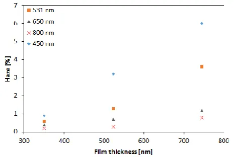
Figure 2 Optical haze for Set D at 4 different wavelengths.
[image:6.595.314.549.498.654.2]The carrier mobility of Set D is fractionally greater than that of the reference TCO sample, while the carrier concentration is lower. The increased optical scatter with film thickness confirms the increased surface roughness, as shown in figure 2. The reference FTO gave haze values comparable to its thickness and
Table 3 Some physical and electrical properties of Set D.
Set D d (nm) RMS (nm) Rs (Ω/sq) µ (cm2/Vs) N/×1020 (cm-3)
D1 350 13 20 28 3.3
D2 523 21 11 31 3.8
D3 745 25 7 34 3.5
d: Average film thickness, AFM – root mean squared (RMS) roughness, Rs:
ARTICLE Journal Name
surface roughness i.e. between the APCVD samples with thicknesses of 350 nm and 523 nm.
As can be seen in Figure 3 there is a general decreased in transmission and increase in absorptance as the films increase in thickness, particularly at the higher wavelengths. The reference FTO generally lies within the band of optical values, except for a much increased reflectance >1500 nm.
In all cases the improved quality of the FTO gave cell efficiencies comparable or better than the cells fabricated from the commercial FTO (Table 4). This must arise from a combination of properties as although Set D all has a lower carrier concentration and higher mobility than the reference, it only has lower sheet resistance for two out of three samples. The over-riding factor is the higher optical transmittance for our samples. Interestingly, as the FTO increased in thickness there was a corresponding increase in cell FF and decrease in Roc
leading to increased efficiency. This is despite decreased transmission in particularly above 1200 nm and a possible issue with increased roughness (25 against 13 nm). This again confirmed that when using a mesoporous scaffold that FTO roughness is not a problem, given that it is possible to provide a conformal, pin hole free BL. This set of results establishes that the overriding FTO property determining the cell efficiency is its sheet resistance.
Figure 3 (a) Transmittance (solid line) and reflectance (dotted line), b) absorptance.
Figure 4 (a) Arrhenius plot of the surface conductivity of sputtered TiO2-x and TiO2
by ALD thin films, showing that the bulk conductivity of these thin films increases with the degree of reduction. (b) Activation energy (Ea) as a function of the partial
O2 pressure (pO2), the blue line corresponds to the 7meV of ALD deposited TiO2-x.
[image:7.595.59.296.372.703.2]Choose of BL deposition method – sputtering vs ALD
As discussed earlier in the paper, deposition of the BL via ALD rather than by spin coating produced more efficient cells. A third technique of magnetron sputtering was used. In both cases TiO2-x layers were ~20 nm thick. As shown in Figure 4a,
TiO2-x by sputtering has an overall dark conductivity (σ dark)
which depends on the degree of reduction, with larger electrical conductivity obtained for films deposited without introducing O2 during the sputtering process. At the same time, the
Arrhenius plot of the surface conductivity show a typical semi-conductive behaviour, with the conductivity increasing with increasing temperature. This indicates that oxygen vacancies act as a dopant in TiO2, as smaller activation energies are found
for TiO2-x films deposited with more reducing conditions (see
Figure 4b). Such behaviour is ascribed to electrical conduction through mid-gap defect states induced by Ti3+ sites.
Interestingly, the TiO2-x deposited by ALD shows a very small
Ea of only 7 meV, which is consistent with a degenerately doped semiconductor. Nonetheless, the absolute value of the σ is comparable with the most stoichiometric TiO2-x film presented
in this study, which is ascribed to the higher density of ALD deposited films. In addition, the optical absorptance of these TiO2-x films is found to increase with the degree of reduction,
showing a broad peak centred around a wavelength of 900 nm, related to the mid-gap optical losses. Following these findings, in devices, the sputtered TiO2-x reference thin films with pO2 =
7.5 x 10⁻⁶ mbar were selected for their optimal
conductivity-transparency trade-off.
As can be seen in Figure 4a and b the lowest conductivity and the smallest optical absorptance was obtained with the TiO2-x by ALD. This would suggest that the ALD TiO2-x contains a
lower level of oxygen vacancies than the sputtered films and hence closer to being stoichiometric. However, previous work has shown that films deposited under these conditions tend to be non-stoichiometric with a significant amount of Ti3+. In
addition use of an amine based precursor leads to unintentional doping by carbon and nitrogen within the film. The high level of impurities leads to a reduction in the film conductivity.
Data from the reference cells (Table 4) showed that sputtered thin films of TiO2-x led to higher Jsc and much lower
Roc, hence higher efficiencies for the sputtered over ALD derived
samples despite slightly lower transparency. This is consistent with the observed electrical conductivities. However, the same trends in cell properties against FTO thickness were seen for both types of deposition. Data from the cells produced from the APCVD FTO showed that sputtering led to cells with similar efficiencies for both thinnest and thickest FTO film, although with slightly higher Roc. However, for the intermediate thickness
FTO the results were much poorer. This is due to the perovskite layer being less compact due to too fast evaporation of the solvent leaving voids and/or a higher resistance in the ALD layer hindering the extraction of electrons. The latter could be a product of the high temperature (500 oC) scaffold anneal,
changing the TiO2-x structure more adversely for ALD than via
sputtering. It is likely on annealing the thin, amorphous ALD crystallises and hence leads to the formation of poor grain boundaries due to the higher level of impurities than those expected in the sputtered film. In addition the annealing could induce cracking of the film.
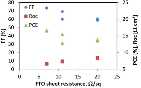
The much improved uniformity of the FTO and BL aided the formation of a better adhered and uniform perovskite layer. This in turn has allowed us to increase the dimensions of the cells for batch from 0.43 cm2 to 1 cm2. As can be seen by the
cell data for Set D the efficiencies are still as high as, if not higher than that produced for the earlier batches using the smaller cell size. As can be seen in Table 4 as the thickness of the FTO layer is increased there is a corresponding improvement in FF and efficiency, while a decrease in Roc. This can be ascribed to the
[image:8.595.57.536.523.744.2]decrease in FTO sheet resistance, which is demonstrated in Figure 5.
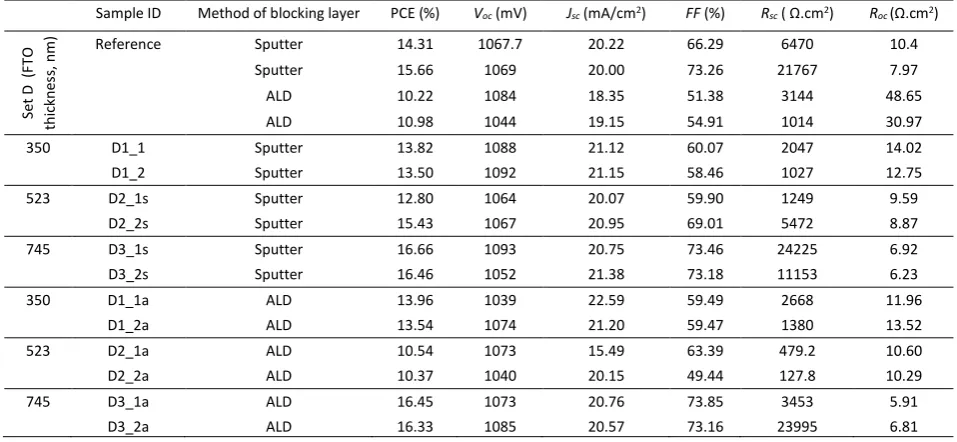
Table 4 Cell data for Set D.
Sample ID Method of blocking layer PCE (%) Voc (mV) Jsc (mA/cm2) FF (%) Rsc ( Ω.cm2) Roc (Ω.cm2)
Se
t D
(
FT
O
thi
ck
ne
ss, n
m
) Reference Sputter 14.31 1067.7 20.22 66.29 6470 10.4
Sputter 15.66 1069 20.00 73.26 21767 7.97
ALD 10.22 1084 18.35 51.38 3144 48.65
ALD 10.98 1044 19.15 54.91 1014 30.97
350 D1_1 Sputter 13.82 1088 21.12 60.07 2047 14.02
D1_2 Sputter 13.50 1092 21.15 58.46 1027 12.75
523 D2_1s Sputter 12.80 1064 20.07 59.90 1249 9.59
D2_2s Sputter 15.43 1067 20.95 69.01 5472 8.87
745 D3_1s Sputter 16.66 1093 20.75 73.46 24225 6.92
D3_2s Sputter 16.46 1052 21.38 73.18 11153 6.23
350 D1_1a ALD 13.96 1039 22.59 59.49 2668 11.96
D1_2a ALD 13.54 1074 21.20 59.47 1380 13.52
523 D2_1a ALD 10.54 1073 15.49 63.39 479.2 10.60
D2_2a ALD 10.37 1040 20.15 49.44 127.8 10.29
745 D3_1a ALD 16.45 1073 20.76 73.85 3453 5.91
ARTICLE Journal Name
The best cell result was obtained from the thickest and hence lowest resistance APCVD FTO layer (7 /sq), with sputtered 20 nm blocking layer with scaffold and 300 nm perovskite layer giving an overall value of 16%, which was confirmed by maximum power point (MPP) tracking for 5 minutes. This compares extremely well with literature results for similar cells, Lee et al16 16.6% although with a much smaller
cell size of 0.16 cm2 and the certificated value reported by
Japan's National Institute for Materials Science of 15%, and similar cell size 1.017 cm2.34 Higher values have been reported
by Yang et al35 at 20% for a 0.096 cm2 cell and Li et al36 19.6 %
although these are not directly comparable as in the former formamidinium lead triiodide was used and the latter mixed anion (formamidinium and methylammonium) as well as mixed halide rather than (in this work) methyl ammonium lead triiodide.
Having achieved this excellent result, further study will be needed to move to planar cells (without the scaffold) as this gives a simpler, cleaner architecture and an easier manufacturing process. For which uniform, highly conformal interfaces will be required to keep a high contact surface area between perovskite and its electron transport layer, while keeping the film pin hole free with low recombination between FTO electrons and perovskite holes.
Conclusions
We have shown the importance of obtaining uniform thin films of FTO, with low sheet resistance to aid formation of pin hole free uniform TiO2-x blocking layers and hence well adhered,
perovskite layers. It has been confirmed that for cells containing scaffolds the FTO roughness (< 33 nm) is not a major issue. The improved layers’ uniformity in turn enabling the formation of large cells (1 cm2) reaching very high efficiency of 16 %.
Optimal BL thickness was 20 nm, while thicker films gave decreased shunt resistance and thinner a greater number of pin holes through the layers. We also showed that the conformal nature of ALD and magnetron sputtering, along with their increased uniformity control over spin coating again improved
cell efficiency. The main improvement comes for the smaller Roc, attributed to an improved electrical transport through
particularly the sputtered TiO2-x blocking layer. It is worth
noticing that a further improvement could be expected by fine-tuning the stoichiometry of sputtered deposited TiO2-x.
Perovskite deposition using higher concentration and low evaporation rate were crucial to producing dense layers with no gaps into the lower layers of the cell structure.
Acknowledgements
This work was financed by Framework 7 grant FP7 NMP.2012.1.4-1 309530 PLIANT “Process line implementation for applied surface nanotechnologies”.
Notes and references
1 A. M. Guloy, Nature 1994, 369, 467-469.
2 A. Krojima, K. Teshima, Y. Shirai and T. Miyasaka, J. Am. Chem. Soc., 2009, 131, 6050-6051
3 M. M. Lee, J. Teuscher, T. N. Murakami and H. J. Snaith, Science 2012, 338, 643-647.
4 H.-S. Kim, C.-R. Lee, J.-H. Im, K.-B. Lee, T. Moehl, A. Marchioro, S.-J. Moon, R. Humphry-Baker, J.-H. Yum, J. E. Moser, M. Gratzel and N.-G. Park, Sci. Rep., 2012, 2, 591.
5 D. P. McMeekin, G. Sadoughi, W. Rehman, G. E. Eperon, M. Saliba, M. T. Horantner, A. Haghighirad, N. Sakai, L. Korte, B. Rech, M. B. Johnston, L. M. Herz and H. J. Snaith, Science 2016,
351, 151-155.
6 W. Chen, Y. Wu, J. Liu, W. Zhang, X. Yang, H. Chen, E. Bi, I. Ashraful, M. Gratzel, L. Hen, Science 2015, 350, 944-948. 7 J.-W. Lee, D.-J. Seol, A.-N. Cho and N.-G. Park, Adv. Mater.,
2014, 26, 4991-4998.
8 M. Saliba, T. Matsui, J.-Y. Seo, K. Domanski, J.-P. Correa-Baena, M. K. Nazeeruddin, S. M. Zakeeruddin, W. Tress, A. Abate, A. Hagfeldt and M. Gratzel, Energy Environ. Sci., 2016,
9 1989-1997.
9 www.nrel.gov/ncpv/images/efficiency_chart.jpg Accessed 16.08.2016.
10 D. S. Bhachu, D. O. Scanlon, E. J. Saban, H. Bronstein, I. P. Parkin, C. J. Carmalt and R. G. Palgrave, J. Maters. Chem. A 2015, 3, 9071-9073.
11 S. Chen, J. Briscoe, Y. Shi, K. Chen, R. M. Wilson, S. Dunn, R. Binions, Cryst. Eng. Comm. 2015, 17, 7486.
12 D. Bi, S.-J. Moon, L. Haggman, G. Boschloo, L. Yang, E. M. Johansson, M.K. Nazeeruddin, M. Gratzel and A. Hagfeldt, RSC Adv. 2013, 3, 18762-18766.
13 M. Anaya, J. F. Galisteo-Lopez, M. E. Calvo, C. Lopez, and H. Miguez, J. Phys. Chem. C 2016, 120, 3071-3076.
14 A. M. A. Leguy, Y. Hu, M. Campoy-Quiles, M. I. Alonso, O. J. Weber, P. Azarhoosh, M. van Schilfgaarde, M. T. Weller, T. Bein, J. Nelson, P. Docampo and P. R. F. Barnes, Chem. Maters., 2015, 27, 3397-3407.
15 W. Tress, N. Marinova, T. Moehl, S. M. Zakeeruddin, M. K. Nazeeruddin and M. Gratzel, Energy Environ. Sci., 2015, 8, 995-1004.
16 Y. H. Lee, J. Luo, R. Humphry-Baker, P. Gao, M. Gratzel and M. K. Nazeeruddin, Adv. Funct. Mater., 2015, 25, 3925-3933. 17 J. Choi, S. Song, M. T. Horantner, H. J. Snaith and T. Park, ACS
Nano, 2016, 10, 6029-6036.
[image:9.595.51.288.275.424.2]18 W. Ke, G. Fang, Q. Liu, L. Xiong, P. Qin, H. Tao, J. Wang, H. Lei, B. Li and J. Wan, J. Am. Chem. Soc., 2015, 137, 6730-6733.
Figure 5 The trend in cell parameters for FTO Set D for the cells fabricated using
the sputtered TiO2-x layer.
5 10 15 20 25 0 10 20 30 40 50 60 70 80
0 5 10 15 20 25
PCE [% ], R o c [ . cm 2] FF [% ]
FTO sheet resistance, /sq
19 J. T. -W. Wang, J. M. Ball, E. M. Barea, A. Abate, J. A. Alexander-Webber, J. Huang, M. Saliba, I. Mora-Sero, J. Bisquert, H. J. Snaith and R. J. Nicholas, Nano Lett., 2014, 14 724-730.
20 D. Liu and T. L. Kelly, Nat. Photonics 2014, 8, 133-138. 21 H. M. Yates, P. Evans, D. W. Sheel, S. Nicolay, L. Ding, C. Ballif,
Surf. Coat. Technol., 2013, 230, 228-233.
22 C. Zuo, H.J. Bolink, H. Han, J. Huang, D. Cahen and L. Ding, Adv. Sci., 2016, 3, 1500324.
23 P. Chen, Y. Wang, M. Wang, X. Zhang, L. Wang and Y. Liu, J. Energy Chem., 2015, 24, 717-721.
24 N. Ahn, D.-Y. Son, I.-H. Jang, S. M. Kang, M. Choi and N.-G. Park, J. Am. Chem. Soc., 2015, 137, 8696-9.
25 H. M. Yates, P. Evans, D. W. Sheel, S. Nicolay, L. Ding and C. Ballif, Surf. Coat. Technol., 2012, 213, 167-174.
26 M.H. Siadati and K.K. Chawla, Mater. Character., 1991, 27, 19-26.
27 M. Afzaal, H.M. Yates and J.L. Hodgkinson, Coatings, 2016, 6, 43-52.
28 S. Faÿ, J. Steinhauser, S. Nicolay and C. Ballif, Thin Solid Films, 2010, 518, 2961-2966.
29 J.Springer, B. Rech, W. Reetz, J. Muller and M. Vanecek, Solmat., 2005, 85, 1-11..
30 M. Ritala and M. Leskela, Nanotechnol., 1999, 10, 19-24. 31 Y.W. Chen, J.D. Prange, S. Duhnen, Y. Park, M. Gunji, C.E.D.
Chidsey and P.C. McIntyre, Nature Mater., 2011, 10, 539-544. 32 F. Di Giacomo, V. Zardetto, G. Lucarelli, L. Cinà, A. Di Carlo, M.
Creatore and T.M. Brown, Nano Energy, 2016, 30, 460–469 33 H. M. Yates, P. Evans, D. W. Sheel, U. Dagkaldiran, A. Gordijn,
F. Finger, Z. Remes and M. Vanecek, Intl. J. Nanotechnol., 2009, 6, 816-827.
34 (a) M. A. Green, K. Emery, Y. Hishikawa, W. Warta and E. D. Dunlop, Prog. Photovol., 2016, 23, 3-11.
35 W. S. Yang, J. H. Yoh, N. J. Jeon, Y. C. Kim, S. Ryu, J. Seo and S. I. Seok, Science 2015, 348, 1234-1237.