© 2015, IRJET.NET- All Rights Reserved
Page 1757
Phase Shifted Full Bridge DC-DC Converter
Arya P S
1, Chithra R
21
M-Tech student , Electrical and Electronics, ASIET, Kerala, India
2Assistant Professor, Electrical and Electronics, ASIET, Kerala, India
---***---Abstract -
This paper deals with the analysis andsimulation of phase shifted full bridge dc-dc converter. The full bridge dc-dc converter with phase shift control has advantages of achieving high efficiency at high operating frequencies, reduced switching losses, low EMI and stress. In this paper a 400V input dc is converter to 12V output dc voltage using this converter. The converter is simulated using PSIM software and compared with conventional full bridge dc-dc converter.
Key Words:
Phase shifted full bridge DC-DC converter,
DC-DC Converter, Zero voltage switching etc…
1. INTRODUCTION
DC-DC converters are used to convert DC voltage from one voltage level to another. They can be step up or step down. Mostly power electronic converters consist of semiconductor switches like MOSFETS and IGBTs. DC-DC converters are classified into non isolated and isolated converters. A transformer is present in the isolated topology which provides isolation between the input and the output. The non isolated converters are buck (step down) converter, boost converter (step up) converter, buck boost converter, and cuk converter. The various isolated converters are forward converter, flyback converter, push pull converter, half bridge converter and full bridge converters.
In recent years the high power isolated DC-DC converters has developed in the market due to its requirement in the applications like fuel cell applications, battery based storage systems and telecommunications systems etc. In most of the applications the transformer is incorporated due to the circuit to provide isolation. The advantages of using isolated are the transformer present in the isolated topology can provide large step up or step down conversion ratio, multiple dc outputs can be obtained by providing multiple secondary windings, voltage and current stress in the transistors can be reduced by proper design of turns ratio.
The basic requirement of converters is small size and high efficiency. To achieve small size high switching frequency operation is necessary but the switching losses increases with increase in switching frequency. The solution for this problem is using soft switching techniques such as ZVS (zero voltage switching) and ZCS (zero current switching). These techniques provide zero voltage or current during switching transitions and thus reduce switching losses.
2. PHASE SHIFTED FULL BRIDGE CONVERTER
Full bridge converter is a buck derived converter. These converters are mostly used in medium to high power applications. The output voltage can be controlled by two methods: PWM control and phase shift control. The full bridge configuration used for high input voltage and in high power applications is the phase shifted full bridge dc-dc converter.
Phase shifted full bridge dc-dc converter (PSFB) is similar to the conventional full bridge dc-dc converter, but with a phase shifting control. In phase shifted full bridge dc-dc converter, the switches attain zero voltage switching which reduces the switching losses. The converter can attain high efficiency at high switching frequencies and also has benefits such as low EMI; low switching noise doesn’t require additional snubber circuits to reduce losses. PSFB converters are used to step down high dc voltages and to provide isolation in medium to high power applications such as renewable energy systems, telecom rectifiers, battery charging systems, server power supplies etc.
2.1. OPERATING PRINCIPLE
© 2015, IRJET.NET- All Rights Reserved
Page 1758
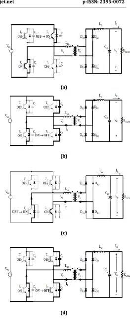
Fig -1: Phase shifted full bridge dc-dc converterThe full bridge inverter consists of four semiconductor switches such as IGBTs or MOSFETs with their diodes. In phase shifted control, the gate signals of T2 and T3 are phase shifted with respect to T1 and T4. The high frequency transformer is used and the high frequency AC voltage at the secondary is rectified using full wave rectifier and filtered using a low pass filter to obtain smooth DC output voltage. The parasitic capacitance (C1, C2, C3, C4) are connected across the switches in figure 1. The inductor connected in series with the primary winding of the transformer emphasizes the leakage inductance of the high frequency transformer. If required additional inductor can be connected in series with the transformer primary winding. The two components, the switch output capacitance and transformer leakage inductance decreases the performance of the converter in hard switching but is utilized advantageously in phase shifted converter to achieve ZVS. Hence attaining ZVS condition and elimination of switching losses, the phase shifted full bridge dc-dc converter topology for medium to high power applications.
2.2. MODES OF OPERATION
The first half cycle modes of operation are explained by 6 circuit modes of operation. The second half cycle the event repeats in the same manner as that of first cycle.
Mode 0
In this mode, the switches T1 and T2 are on and power is
transferred from input to output. The mode is shown in fig 2(a).
(a)
(b)
(c)
© 2015, IRJET.NET- All Rights Reserved
Page 1759
(e)(f)
Fig -2: Modes of operation
Mode 1
In mode 1, the switch T1 is turned off and the primary
current flows through C1 and C4. The primary current
charges C1 to VDC and discharges C4 to zero. The energy
required to charge and discharge is provided from the energy stored in the leakage inductor Llk.
Mode 2
In mode 2, the capacitor C4 is discharged to zero and the
freewheeling diode DR4 of switch T4 is forward biased and
starts conducting. Beyond this, the switch T4 can be turned
on with zero voltage across it and zero voltage switching turn on can be obtained. This is shown in fig 2(c).
Mode 3
In this mode, switch T2 is turned off and the primary
current flows through the capacitors C2 and C3. This
current charges C2 and discharge C3. The capacitor charges
to VDC and the capacitor C3 discharges to zero. This is
shown in fig 2(d). The energy required to charge and discharge the capacitors are provided by not only the
leakage inductance of the transformer but also the energy stored in the output inductor.
Mode 4
At the end of this mode, the capacitor completely discharges to zero. The freewheeling diode DR3 of switchT3
becomes forward biased and starts to conduct. The switch T3 is turned on with zero voltage across the switch and the
ZVS condition satisfied. This is shown in fig 2(e). All the rectifier diodes are conducting in this mode so the secondary winding of the transformer is short circuited.
Mode 5
In this mode, the current that flows through the diodes DR1
and DR2 decreases to zero. The load current flows through
DR2 and DR4 as shown in fig 2(f). So the secondary voltage
builds up again and the output filter stores energy while power is transferred from input to the output. The cycle repeats and the zero voltage switching is obtained in all the switches of the converter.
Hence in phase shifted full bridge dc-dc converter, the ZVS condition is achieved in both the inverter legs.
© 2015, IRJET.NET- All Rights Reserved
Page 1760
3. EXPERIMENTAL RESULTS
The phase shifted full bridge dc-dc converter is simulated using PSIM software with parameters as follows:
Input voltage Vs = 400V
Output voltage Vo = 12V
Switching frequency Fs = 100 kHz
The proposed converter was simulated using the parameters to verify the operating principle, advantages and performance efficiency of the converter. The conventional full bridge dc-dc converter is compared with the phase shifted full bridge dc-dc converter and the advantage ie, the zero voltage switching was obtained. From the comparison between the two converters, it was found that the phase shifted full bridge dc-dc converter has reduced switching and conduction losses and higher efficiency as compared to the full bridge dc-dc converter. The simulation model and the results are shown below.
Fig -4: PSIM Model of phase shifted full bridge dc-dc converter
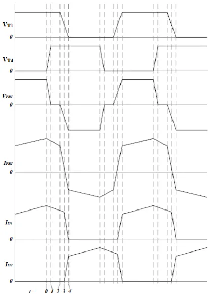
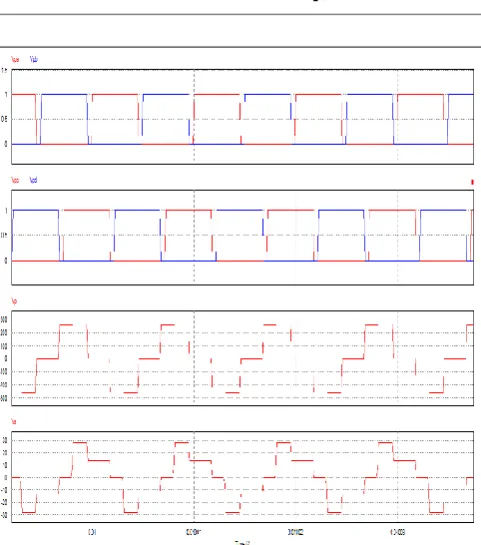
3.1. WAFEFORMS
The figures 5, 6, 7 shows the key waveforms of phase shifted full bridge dc-dc converter. The primary and secondary voltages with the input voltage of 400V and output voltage of 12V are as shown in figure 5. The output voltage waveforms are shown in figure 6 and figure 7 shows the zero voltage turn on of the switch.
Fig -5: Waveforms: Vpa, Vpb, Vpc, Vpd- switching pulses, Vp, Vs- primary and secondary voltages of transformer.
Fig -6: Output voltage
Fig -7: Vpa: pulse of switch, Va: voltage across switch.
© 2015, IRJET.NET- All Rights Reserved
Page 1761
4. CONCLUSION
This paper has presented the phase shifted full bridge dc-dc converter which can solve the problems of full bridge dc-dc converter such as high switching losses, conduction losses, high EMI and lower efficiency. The theoretical analysis of the phase shifted full bridge dc-dc converter is presented to show the advantage of phase shifted full bridge dc-dc converter over traditional full bridge dc-dc converter. The experimental results are shown in the figures above which clearly show the advantages of the proposed converter and zero voltage switching is obtained which improves the efficiency of the converter. The phase shifted full bridge converter is used in medium to high voltage applications such as power supplies, battery chargers, renewable systems etc.
REFERENCES
[1] Ned Mohan, Power electronics, converters, application and design, Media Enhanced Third Edition, 2012.
[2] “Phase-Shifted Full-Bridge, Zero-Voltage Transition Design Considerations”, Application Report SLUA107A August 2011.
[3] Sam Abdel-Rahman, “Design of Phase Shifted Full-Bridge Converter with Current Doubler Rectifier”, Design Note DN 2013-01 V1.0 January 2013.
[4] Naga Brahmendra G,"A new active soft-switching circuit for full bridge converters", IEEE International Conference on Power Electronics, Drives and Energy Systems December16-19, 2012, Bengaluru.
[5] Hyun-Lark Do , "A Soft-Switching DC/DC Converter With High Voltage Gain", IEEE Transactions on power electronics, Vol. 25, no. 5, May 2010.
[6] Dunisha S. Wijeratne and Gerry Moschopoulos,"A ZVS-PWM Full-Bridge Converter with Reduced Conduction Losses", IEEE Trans. Power Electron. vol. 29, no. 7, July 2014.
[7] G. N. B. Yadav and N. Lakshminarasamma, "A new active soft switching circuit for full bridge converters," in Proc. IEEEInt. Conf.Power Electron, Drives Energy Syst., Dec.2012.
BIOGRAPHIES
Arya P S was born in Kerala, India in 1990. She received her B.Tech. in Electrical and Electronics Engineering from METS School of Engineering in 2012. She is currently pursuing M.Tech. in Power Electronics and Power System at Adi Shankara Institute of Engineering and Technology, Cochin.
Chithra R was born in Kerala, India. She received her B.Tech degree from Vishwajyothi college of Engineering. She received M.tech. degree from Anna University. She is currently working as an Assistant professor in Adi Shankara Institute of Science and Technology, Kalady.