Available Online At www.ijpret.com
INTERNATIONAL JOURNAL OF PURE AND
APPLIED RESEARCH IN ENGINEERING AND
TECHNOLOGY
A PATH FOR HORIZING YOUR INNOVATIVE WORK
SINUSOIDAL PULSE WIDTH MODULATION APPROACH TO STACKED MULTICELL
CONVERTER (SMC)
RITESH C. UJAWANE1, P.M. MESHRAM2
1. PG Students of Yeshwantrao Chavan College of Engineering, Nagpur.
2. Faculty in Yeshwantrao Chavan College of Engineering, Nagpur.
Accepted Date:
27/02/2013
Publish Date:
01/04/2013
Keywords
Multilevel Inverter
topology,
Stacked Multicell
Converter (SMC),
Multicarrier Sinusoidal
Pulse Width Modulation
(SPWM)
Corresponding Author Mr. Ritesh C. Ujawane
Abstract
Multilevel converter topologies are very important in the areas of
medium and high voltage applications. This paper presents the
Multilevel Inverter topology so called Stacked Multicell Converter which
is derived topology of the conventional Flying Capacitor Multilevel
Inverter topology. The Level Shifted Multicarrier Sinusoidal Pulse Width
Modulation technique is used for the generation of firing signals for
Stacked Multicell Converter (SMC). The Stacked Multicell Converter
topology of Multilevel Inverter causes increase in the number of output
voltage levels with less THD, natural self balancing of flying capacitors
voltage, increase redundancy to obtained desired voltage level,
reduction in the voltage ratings of capacitorsand semiconductor losses.
The proposed topology is simulated using MATLAB Software package
and simulation results are presented to validate the effectiveness and
advantages of the proposed Stacked Multicell Converter (SMC)
Available Online At www.ijpret.com I. INTRODUCTION
The Multilevel Voltage Source converter
topologies are best suited for the medium
and high voltage applications in the
industries. The term multilevel inverter
starts from the three levels [3]. The main
purpose of using a Multilevel Inverter is to
synthesize nearly sinusoidal voltage.
Multilevel inverters have the capability to
handle the voltage in the range of KV and
Megawatts with medium voltage
semiconductors [2]. Multilevel inverter
includes an array of power semiconductors
and capacitor voltage sources, the output of
which generate voltages with stepped
waveforms. The commutation of the
switches permits the addition of the
capacitor voltages, which reach the high
voltage at the output, while the power
semiconductors must withstands only
reduced voltages [4].
This paper presents the Stacked Multicell
Converter topology of multilevel inverter
which is the extended version of
conventional Flying Capacitor Multilevel
Inverter topology. The multicarrier
sinusoidal pulse width modulation
technique for SMC is given. The three
conventional topologies and Stacked
Multicell Converter topology performances
is compared on the basis of output voltage
THD and
Fundamental output voltages of the
Multilevel Inverter topologies [1].
II. MULTILEVEL INVERTER TOPOLOGIES
Basically there are three conventional
topologies of Multilevel Inverter as follows;
[A] Diode clamped or Neutral point
clamped Multilevel (NPC) Inverter.
[B] Capacitor clamped or Flying capacitor
Multilevel (FCM) Inverter.
[C] Cascaded converter (CC).
A. Neutral Point Clamped (NPC) Multilevel
Inverter
An m-level diode clamped converter
typically consists of m-1 capacitors on the
dc bus and produces m levels of the phase
voltage. Fig. 1 shows the three level diode
clamped multilevel inverter in which the dc
bus consist of two capacitors, C1, C2. For a
dc bus voltage Vdc, the voltage across each
capacitor is Vdc/2, and each device voltage
stress will be limited to one capacitor
voltage level, Vdc/2, through clamping
Available Online At www.ijpret.com
Fig. 1 Three-level-Diode Clamped
Multilevel Inverter
Advantages of diode clamped Multilevel
Inverter is as follows.
• When the numbers of output voltage
level is high, harmonic distortion will be
less.
• Efficiency is high because all
semiconductor devices are operated at
the fundamental frequency.
• Reactive power flow can be controlled.
• The control strategy is simple for a
back-to-back intertie system.
Disadvantages:
• Number of clamping diodes is more
when the number of output voltage
levels is high.
• Complications in real power flow
control for the individual converter.
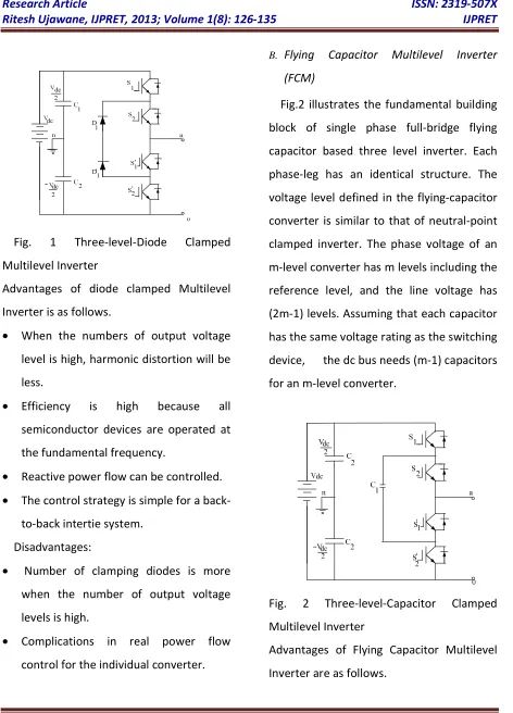
B. Flying Capacitor Multilevel Inverter
(FCM)
Fig.2 illustrates the fundamental building
block of single phase full-bridge flying
capacitor based three level inverter. Each
phase-leg has an identical structure. The
voltage level defined in the flying-capacitor
converter is similar to that of neutral-point
clamped inverter. The phase voltage of an
m-level converter has m levels including the
reference level, and the line voltage has
(2m-1) levels. Assuming that each capacitor
has the same voltage rating as the switching
device, the dc bus needs (m-1) capacitors
for an m-level converter.
Fig. 2 Three-level-Capacitor Clamped
Multilevel Inverter
Advantages of Flying Capacitor Multilevel
Available Online At www.ijpret.com
• Capacitor voltages provides extra ride
through capabilities during power
failure.
• Redundancy (Switching combination)
for balancing different voltage levels.
• When the number of levels is high,
harmonic content will be low to avoid
the need for filters.
• Both real and reactive power flow can
be controlled.
Disadvantages:
• Large number of storage capacitors is
required when the number of converter
levels is high.
• The inverter control will be very
complicated, and the switching
frequency and switching losses will be
high for real power transmission.
C. Cascaded converters
The cascaded converter can avoid extra
clamping diodes or voltage balancing
capacitors. Fig.3 shows five level cascaded
H-bridge converters with separate dc
source. The ac terminal voltage of different
level inverters is connected in series. Each
H-bridge inverter generates three level
outputs, +Vdc, 0, and –Vdc. This is made
possible by connecting the dc sources
sequentially to the ac side via the four
gate-turn-off devices. Minimum harmonic
distortion can be obtained by controlling
the conducting angles at different inverter
levels.
Fig. 3 Five-level- Cascaded Full H-Bridge
Converter
Advantages of Cascaded Converters are as
follows;
• Least numbers of components
required, compare to all multilevel
topologies to achieve the same number
of voltage levels.
• Modularized circuit layout and
packaging is possible because each level
has the same structure, and there are
no extra clamping diodes or voltage
Available Online At www.ijpret.com
• Soft switching can be used in this
topology.
Disadvantages:
• Separate dc sources are required for
real power conversions, and thus
limitations in application of this
topology.
III. STACKED MULTICELL CONVERTER (SMC)
A SMC is an inverter (DC-AC Converter)
for high voltage applications. The topology
of this inverter is made up of by m×n array
of cells, see Fig.4. this configuration allows
to share the total voltage and current
stresses among the switches. Then it is
possible to use conventional
semiconductors to handle high output
power. The application area for SMC can be
found in applications such as UPS, Switching
Power Supplies, DSTATCOM, etc.
Fig.4 2×3- cell- 7 level Stacked Multicell
Converter
Stacked Multi-cell Converter is proposed to
increase the no. of output voltage levels
and as a result, reduced the output voltage
THD with reduced ratings and losses of
flying capacitors and semiconductors [1][6].
A 2×3-Cell-7-level single phase stacked
multicell converter is shown in figure above
where, m = no. of stacks (rows) and n = no.
of columns (stage). SMC is based on
associations of basic switching cells
connected in series. Each one of these
switching cells is built with two switches.
The basic switching cells have
complementary states. It means, that only
one switch is conducting at a given time.
The association of these switching cells
allows the voltage to be distributed among
the switches, giving better output
waveforms in terms of the number of levels
used. To ensure its functionality, a SMC
used capacitors like intermediate voltage
sources. This is due to the fact that
switching cells only work if they are being
powered by flying voltage sources without
Available Online At www.ijpret.com
uses m×n=6 switching cells and (n-1) × m =
4 flying capacitors.
The voltage across each capacitor is equal
to;
V=i×E/m×n
Where, E is the total input voltage of the
converter.
The No. of configuration states in a SMC
is equal to:
Nconfig = (n+1) m
For 2×3 SMC, sixteen states can be
obtained; this means that each states
generates different voltage levels at the
output. However, even sixteen states are
possible; some of them have the same
output voltage. These states can or not be
used depending on the control strategy.
For m×n SMC the maximum number of
output voltage level is given by:
Nlevel = (m×n)+1
For SMC structure the complexity of control
is based on a PWM strategy.
The blocking voltage for each switching
device is:
Vswitch =E/m×n
IV. MULTICARRIER SINUSOIDAL PULSE
WIDTH MODULATION (LEVEL SHIFTED
SPWM)
The multicarrier sinusoidal pulse width
modulation technique have three very
simple dispositions that seem the most
interesting:
1) All the carriers are alternatively in
opposition (APODPWM) as shown in Fig.
5, with this method the most significant
harmonics are centred as side bands
around the carriers.
0 0.002 0.004 0.006 0.008 0.01 0.012 0.014 0.016 0.018 0.02 -2
-1.5 -1 -0.5 0 0.5 1 1.5 2
Time(sec)
A
m
p
li
tu
d
e
Fig. 5 Alternate Phase Opposition
Disposition PWM
2) All the carriers above zero value
reference are in phase among them but
in opposition with those below
(PODPWM) as shown in Fig. 6, the
significant harmonics are located
around the carrier frequency, for both
phase and line-to-line voltage
Available Online At www.ijpret.com
0 0.002 0.004 0.006 0.008 0.01 0.012 0.014 0.016 0.018 0.02 -2
-1.5 -1 -0.5 0 0.5 1 1.5 2
Time(sec)
A
m
p
lit
u
d
e
Fig. 6 Phase Opposition
Disposition PWM
3) All the carriers are in phase (PDPWM),
for this technique, significant hormonic
energy is concentrated at the carrier
frequency, but since it is the co-phasel
component, it does not appear in the
line-to-line voltage, PDPWM is as shown
in Fig. 7,
0 0.002 0.004 0.006 0.008 0.01 0.012 0.014 0.016 0.018 0.02 -2
-1.5 -1 -0.5 0 0.5 1 1.5 2
Time(sec)
A
m
p
li
tu
d
e
Fig. 7 Phase Disposition PWM
V. SIMULATIONRESULTS
In this section, in order to verify the good
performance of proposed topology
configuration, a computer simulation is
provided. The topologies are simulated
using MATLAB software. The parameters
used in simulation are given in table I. The
simulation results are presented for
conventional topologies of Multilevel
Inverters and proposed Stacked Multicell
Converter (SMC). Table 2 shows the
performance comparison of different
topologies of Multilevel inverter on the
basis of fundamental output voltage and
THD.
TABLE I
PARAMETERSUSEDFORSIMULATION
Parameters values
DC voltage 100 V
Fundamental
switching frequency
50Hz
Resistive- Inductive
load
1Ω, 1mH
Switching frequency
of converter (fswitching)
2kHz
Available Online At www.ijpret.com
TABLEII
SUMMARY OF SIMULATION RESULTS FOR
DIFFERENT MULTILEVEL INVERTER
TOPOLOGIES
Topology Fundamental
RMS Output
Phase Voltage
in Volts
(Three Level) THD Neutral-Point Clamped 53.19 84.82 Flying Capacitor 58.54 73.49
Cascaded 68.2
57.38
Stacked
Multicell
69.99
18.81
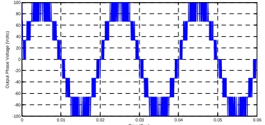
0 0.01 0.02 0.03 0.04 0.05 0.06 -100 -80 -60 -40 -20 0 20 40 60 80 100 Time (Sec) O u tp u t P h a s e V o lt a g e ( v o lt s )
Fig. 8 Output Phase Voltage of
Three-level-Neutral-Point Clamped Multilevel Inverter
0 0.01 0.02 0.03 0.04 0.05 0.06
-100 -80 -60 -40 -20 0 20 40 60 80 100 Time (Sec) O u tp u t P h a s e V o lt a g e ( V o lt s )
Fig. 9 Output Phase Voltage of
Three-level-Capacitor Clamped Multilevel Inverter
0 0.01 0.02 0.03 0.04 0.05 0.06 -100 -80 -60 -40 -20 0 20 40 60 80 100 Time (Sec) O u tp u t P h a s e V o lt a g e ( V o lt s )
Fig. 10 Output Phase Voltage of
Three-level Cascaded MultiThree-level Inverter
0 0.01 0.02 0.03 0.04 0.05 0.06
-100 -80 -60 -40 -20 0 20 40 60 80 100 Time (Sec) O u tp u t P h a s e V o lt a g e ( V o lt s )
Fig. 11 Output Phase Voltage of 2×3- 7-
level Stacked Multicell Inverter
Available Online At www.ijpret.com
CONCLUSION
The performance of the conventional
Multilevel Inverter topologies like
Neutral-Point clamped Multilevel Inverter, Flying
Capacitor Multilevel Inverter, Cascaded
Multilevel Inverter have been checked with
carrier based sinusoidal pulse width
modulation. The extended version of flying
capacitor Multilevel Inverter the Stacked
Multicell Converter have also been
examined to the carrier based sinusoidal
pulse width modulation. The quality of the
spectrum performance of the output
waveform is checked by THD and utilization
of the input DC voltage is checked by
fundamental values of the output AC
voltage. In level shifted modulation
techniques that is PD, POD, and APOD the
THD for out of three, the THD is found to be
least with PDPWM. The fundamental value
of phase voltage is found maximum in
Stacked Multicell Converter Configuration.
REFERENCES
1. Meisam Sadeghi, Amin Nazarllo, Sayed
Hosseini, Ebrahim Babaei, “ A New
DSTATCOM Topology Based on Stacked
Multicell Converter,” IEEE 2nd Power
Electronics, Drives Systems and
Technologies Conference, pp.205-210,
2011.
2. Pablo Lezana, Jose Rodriguez, “ Mixed
Multicell Cascaded Multilevel Inverter,”
IEEE, pp.509-514, 2007.
3. Jose Rodriguez, Jih-Sheng Lai and Fang
Zheng, “Multilevel Inverters: A Survey of
Topologies, Controls, and applications,”
IEEE Trans. Industrial Electronics, vol. 49,
no. 4, pp.724-738, August 2002.
4. J.S. Lal, F.Z. Peng, “Multilevel converters -
A new breed of power converters,” IEEE
Trans. Industrial Electronics, vol. 44, no.
3,pp 356-364, Jun. 1997.
5. Giuseppe Carrara, Simone
Gardella,Mario Marchesoni,Member, “A
New Multilevel PWM Method: A
Theoretical Analysis” IEEE Trans. On power
electronics, vol. 7, no.3, pp.497-505, July
1992.
6. Jose Mariano Fernandez Nava, Pedro
Banuelos Sanchez, “Stacked Multicell
Converter Controlled by DSP” Proceedings
Available Online At www.ijpret.com
Electronics, Communication and computers,
2004.
7. Georgios S. Konstantinou and Vassilios G.
Agelidis, “Performance Evaluation of
Half-Bridge Cascaded Multilevel Converters
Operated with Multicarrier Sinusoidal PWM