NAN O R EVIE W
Open Access
Conductance Quantization in Resistive
Random Access Memory
Yang Li
1,2, Shibing Long
1,2*, Yang Liu
3, Chen Hu
3, Jiao Teng
3, Qi Liu
1,2, Hangbing Lv
1,2, Jordi Suñé
4and Ming Liu
1,2*Abstract
The intrinsic scaling-down ability, simple metal-insulator-metal (MIM) sandwich structure, excellent performances,
and complementary metal-oxide-semiconductor (CMOS) technology-compatible fabrication processes make
resistive random access memory (RRAM) one of the most promising candidates for the next-generation memory.
The RRAM device also exhibits rich electrical, thermal, magnetic, and optical effects, in close correlation with the
abundant resistive switching (RS) materials, metal-oxide interface, and multiple RS mechanisms including the
formation/rupture of nanoscale to atomic-sized conductive filament (CF) incorporated in RS layer. Conductance
quantization effect has been observed in the atomic-sized CF in RRAM, which provides a good opportunity to
deeply investigate the RS mechanism in mesoscopic dimension. In this review paper, the operating principles of
RRAM are introduced first, followed by the summarization of the basic conductance quantization phenomenon in
RRAM and the related RS mechanisms, device structures, and material system. Then, we discuss the theory and
modeling of quantum transport in RRAM. Finally, we present the opportunities and challenges in quantized RRAM
devices and our views on the future prospects.
Keywords:
Resistive random access memory (RRAM), Resistive switching (RS), Conductive filament (CF),
Conductance quantization
Review
Introduction
The persistent perusing of massive storage volume has been
driving the scaling-down process of memory devices for
de-cades. Memories characterized by low-power consumption
and low fabrication cost are needed. Predominant flash
memory has met a scaling-down limitation around 10-nm
magnitude [1, 2]. Therefore, intensive studies have been
carried out in seeking for the next-generation memories.
Resistive random access memory (RRAM) has become one
of the most promising candidates for the next-generation
memory [3
–
14] because of the intrinsic excellent scalability,
simple metal-insulator-metal (MIM) structure, low
fabrica-tion cost, 3D integrafabrica-tion feasibility, and promising
perfor-mances in speed, power, endurance, retention, etc. RRAM
stores information based on the resistive switching effect.
Under appropriate external electrical field, the resistance
state of the RRAM device can be reversibly switched
between a high resistance state (HRS) or OFF-state and a
low resistance state (LRS) or ON-state. There are two
resistive switching modes, i.e., unipolar and bipolar
switch-ing operations under the same or opposite bias polarities,
respectively, which are closely related to the different
ma-terial systems and the different switching mechanisms.
The resistive switching can be a uniform or localized
phenomenon. Uniform switching proportionally scales with
the total area of the switching material, while localized
switching is usually based on the formation and disruption
of conductive filament (CF).
Abundant resistive switching materials, electrode
mate-rials, and their various interfaces are involved in RRAM
switching mechanisms which are rather complex. Rich
electrical, thermal, magnetic, and optical effects are
therefore presented. Typical physical/chemical effects
accompanied in resistive switching processes and in
HRS/LRS states include electrochemical/thermochemical
reactions [15
–
27], metal-insulator transition [28, 29],
magnetic modulation [30
–
47], etc. In this regard, the
RRAM device can serve as a rich platform for studying
the multiple physical/chemical effects. In the CF-type
* Correspondence:[email protected];[email protected]1Key Laboratory of Microelectronics Devices and Integrated Technology,
Institute of Microelectronics, Chinese Academy of Sciences, Beijing 100029, China
Full list of author information is available at the end of the article
RRAM device, when the CF in the resistive switching
(RS) layer is formed, RRAM changes to LRS. If the CF is
ruptured, the device switches back to HRS. The
forma-tion and rupture of the CF can be understood as caforma-tion
or anion migration under applied voltage companied by
electrochemical reaction of the metal or oxygen
vacan-cies. Therefore, CF is believed to be consisted of metal
or oxygen vacancies. The dimension of the CF can be
electrically modulated to be in the order of several tens
to a few nanometers, which has been evidenced by the
observation of high-resolution transmission electron
mi-croscopy (HRTEM) [20, 48
–
60], scanning TEM (STEM)
[59], and atomic force microscopy (AFM) [61
–
63]. In
the localized filamentary switching, the scaling down of
the RRAM device [64] would not influence its memory
characteristics until the area is approaching the CF
mag-nitude. As the CF size is in the range of nanoscale to
atomic size, which is comparable to the mean free path
(Fermi wavelength) of conduction electron, the
scatter-ing might be absent, resultscatter-ing in ballistic electron
trans-port [65] and the quantized conductance (QC) [66
–
68].
In recent studies, conductance quantization phenomena
have been proved to exist in the atomic-sized CF in
RRAM [69
–
72], and the interest for studying them
con-tinues. Revealing the QC effect is of great significance to
deeply understand the physics of RS mechanism in
mesoscopic dimension, which is important to control
the performance, reliability, and variability [73, 74] of
RRAMs and to advance their practical application as
non-volatile memories. At the same time, if the
conduct-ance quantization behaviors can be well modulated, it in
turn can be utilized to realize the multi-level storage
for ultra-high-density memory applications. Thus,
sum-marizing and discussing the QC effect in RRAM is very
necessary. In this review paper, we focus our attention
on the recent development of the research on the QC
effect in CF-based non-volatile RS devices including
basic QC phenomenon in RRAM, RS mechanisms,
device structures, materials, theory, and modeling of
conductance quantization in RRAM.
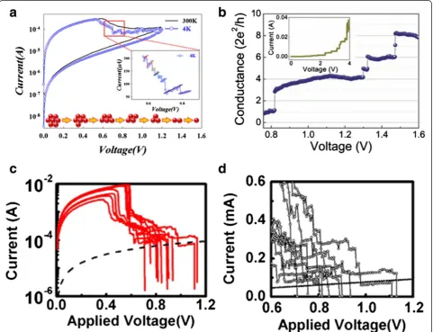
Operating Principles and RS Mechanism of RRAM
In RRAM cell with MIM structure, non-volatile data
storage is achieved through the reversible resistive
switching between HRS and LRS, which are utilized to
store the digits
“
0
”
and
“
1.
”
RS is often based on the
cre-ation and partial destruction of CF. Dependent on the
polarity of the external electrical field, RS is usually
clas-sified into two modes, unipolar and bipolar switching.
The transition from HRS to LRS and that from LRS to
HRS are called as the SET and RESET switching,
respectively. In some cases, if the prepared RS layer in
fresh cell is very insulating with low amount of defects, a
forming process with high voltage is necessary to soft
breakdown the RS layer to trigger the subsequent
repro-ducible RESET and SET switching. Figure 1 shows the
schematic
I
–
V
curves in RS and the corresponding states
of CF-type RRAM device.
Compared with the prototypical non-volatile memories
(NVMs) such as magnetic random access memory
(MRAM) based on the giant or tunneling
magnetoresist-ance effect [75
–
79] and phase change random access
memory (PRAM) based on the reversible phase transitions
between amorphous and crystalline states of phase change
materials [80
–
84], RRAM, an emerging NVM, has shown
various complex resistive switching mechanisms, which is
closely dependent on the different types of switching layer
and electrode materials and also dependent on the
differ-ent operation methods [85
–
87]. To date, the resistive
switching mechanism in RRAM has been widely accepted
to be mainly attributed to the reduction/oxidation (redox)
electrochemistry mechanism, which can operate in the
bulk RS layer, along CFs in the RS layer, and/or at the RS
layer/metal contact interfaces in the MIM structure.
Redox-based RRAM [3, 15, 19, 88
–
95] can be further
clas-sified into two main types,
“
nanoionic
”
(including
electro-chemical metallization (ECM) [17
–
20, 90, 94, 96
–
101]
and valence change mechanism (VCM) [5, 51, 61, 91,
102
–
112]) and
“
thermochemical mechanism (TCM)
”
(i.e.,
fuse/antifuse) [91, 113, 114]. In ECM and VCM devices,
the diffusion or drift of charged species (Ag
+or Cu
+cat-ions), O anions or oxygen vacancies (Vos) in the RS layer
are driven by the ion drift/redistribution and the redox
electrochemistry mechanisms under an electrostatic drift
field. While in TCM devices, it is driven by a thermal
gra-dient diffusion mechanism. In fact, in a practical RRAM
device, the RS process is very complicated, with multiple
mechanisms simultaneously existing, but a certain one is
predominant. It is worth pointing out that TCM is
some-times confused with unipolar VCM. In some cases, the
ECM device is also called as conductive bridge random
access memory (CBRAM) [115
–
119], programmable
metallization cell (PMC) [120
–
122], and atomic switch
[115
–
119, 123, 124]. If TCM dominates the RS, the
resist-ance switching is unipolar. On the contrary, if ECM or
VCM is dominant, the switching is usually bipolar. ECM
devices are cation migration-based RRAMs, while VCM
and TCM devices can be summed up into anion
migration-based RRAMs. Plenty of dielectric materials
have been found to show the redox-based resistance
switching effect, including perovskites, solid-state
electro-lytes, chalcogenides, transition metal oxides, silicon
diox-ide, metal nitrides, organic complexes, polymers, etc.,
among which HfO
2and TaO
xare most widely investigated
Except the redox RS mechanism, the insulator-metal
transition (IMT) or Mott transition in MIM structure
can also contribute to RS effect. The corresponding
re-sistive switching device is called as Mott memory and
sometimes referred as correlated electron random access
memory (CeRAM). In this type of memory device, the
charge injection under the external electrical field
in-duces the transition from weakly correlated electron
state to strongly correlated electron state, which is
acti-vated by a critical electron population [125
–
127].
Elec-tronic switches and memory elements based on the
Mott transition have been explored using several typical
material systems involved in Mott memory including
VO
2[128, 129], NiO [126, 127, 130], SrTiO
3[131],
SmNiO
3[132], etc. The quasi two-dimensional electron
gas (2DEG) formed at the interface between complex
oxides has also been reported to show the
metal-insulator transition effect [133
–
136]. However, in this
paper, we will focus on the redox-based filamentary RS
mechanisms that have been shown to support the
con-ductance quantization effect.
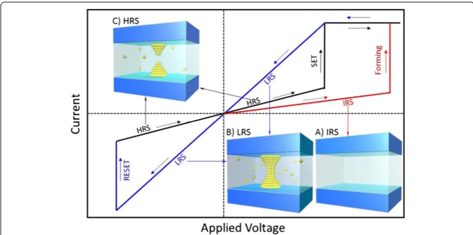
Conductance Quantization in RRAM
The size of the CF can be modulated to the range of
nanoscale to atomic size in both RESET and SET
process. The modulation process can be achieved
through specific electrical operations, especially in the
RRAM devices showing progressive RESET/SET behavior
[137]. This is similar to the performance of memristor
[6, 138
–
142]. When CF is controlled to be thin
enough to show atomic size, the quantum-sized effect
[69] will appear in the CF-type RRAM devices.
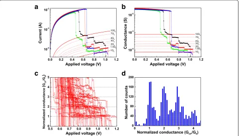
Con-ductance quantization phenomenon is an important
representation of quantum-sized effect. Figure 2 gives
an example of conductance quantization behavior
ob-served in RRAM. The measured current
–
voltage (Fig. 2a)
and corresponding conductance-voltage curves (Fig. 2b)
show that the conductance quantization phenomenon
ap-pears in the RESET process of a Pt/HfO
2/Pt unipolar
RRAM device. Obvious quantized conductance steps with
multiples of
G0
can be observed, in other words, abrupt
conductance transitions of the order of
G0
between
well-defined discrete states can be found in the final stages of
the RESET transient.
G0
= 2
e
2/
h
is the quantum of
con-ductance, with the value of 12.9 k
Ω
−1or 77.5
μ
s, where
e
is the electron charge and
h
is Planck
’
s constant.
Quantized conductance observed in the practical
materials usually presents fluctuation with a certain
degree, so statistical analysis on plenty of
experimen-tal data is often made use of to intrinsically reveal
[image:3.595.56.537.88.327.2]Table 1
The classification of redox-based resistive switching mechanisms and operation principles of redox-based RRAM
Switching mechanism
Electrochemical metallization (ECM) Valence change mechanism (VCM) Thermochemical mechanism (TCM)
Dominating charged species
Metal cations O anions or oxygen vacancies (Vo) O anions or oxygen vacancies (Vo)
Intrinsic nature of CF
Metal CF Vo-CF (bipolar) Vo-CF (unipolar)
Dominating driving force
External electric field External electric field Thermal gradient
Primary operation principle
SET process: (1) The active TE material (Ag, Cu, Ni) in the interface is oxidized under positive electric field; (2) the cations (Ag+, Cu+or Cu2+, Ni+) drift into the RS layer; (3) the
cations are reduced back from the BE/RS-layer interface or from the bulk RS layer or even from the TE/RS layer, depending on the difference between the drift velocity of cations and electrons; (4) metal CF is formed to connect BE and TE, with the reduction process continuing.
SET process: (1) Under positive electric field, TE material in the TE/RS-layer interface is oxidized and O2−/Vo is generated; (2) O ions drift to TE or O vacancies drift to BE through the RS layer to form Vo-CF. The valence states of corresponding cations are changed.
SET (antifuse) process: O vacancies are generated, diffused, and redistributed to form Vo-CF in the bulk RS layer under the thermal gradient induced by electric field. The valence states of corresponding cations are changed.
RESET process: Under the opposite electric field, the metal atoms in the CF are oxidized and drift away, thus CF is partially ruptured.
RESET process: Under the opposite electric field, O ions migrate back to the bulk RS layer to recombine with O vacancies in the CF, thus CF is partially ruptured.
RESET (fuse) process: CF is ruptured or fused as a result of joule heating along the CF through the thermal diffusion process of O vacancies.
Typical RS materials Ion-conducting solid electrolyte (sulfides, selenides, or telluride of Ge, As, Sb, or Ga) such as Ag2S [53], GeSe [224],
Cu2S [172,225], Ag2Se [226], Ag-Ge-Se [227],
(AgI)0.5(AgPO3)0.5[228], etc.; Binary or complex oxides such
as HfO2[215,222,229,230], ZrO2[231,232], SiO2[233], WO3
[234], TaOx[235], GdOx[236], etc.
Transition metal oxides (TMOs) such as TiO2[51,87], HfO2
[106], ZrO2[112], SrTiO3[5,61], TaOx[102], WO3[111], etc.;
doped SiO2[104,107–109]; amorphous C [103,105,110], etc.
Transition metal oxides (TMOs) such as HfO2[69,
70,216,237], NiO [22,238–244], CoO [245], CuO [246], Fe2O3[247], etc.
Typical electrode materials
(1) Top electrode (TE): an electrochemically active metal such as Ag, Cu, and Ni.
(1) Top electrode (TE): a low work function metal not easily reduced back after oxidation, such as Ti, Al, and Nb.
(1) Top electrode (TE): inert electrodes such as Pt, Pd, Ir, Ru, W, Au, etc.
(2) Bottom electrode (BE): an electrochemically inert counter electrode such as Pt, Pd, Ir, Ru, W, Au, etc.
(2) Bottom electrode (BE): inert electrodes, such as Pt, Pd, Ir, Ru, W, Au, etc.
(2) Bottom electrode (BE): inert electrodes such as Pt, Pd, Ir, Ru, W, Au, etc.
Dominating material Electrode RS layer and electrode RS layer
Research
Letters
(2015) 10:420
Page
4
of
(Cu/HfO2/Pt) (Ti/HfO
2/Pt) (Pt/HfO2/Pt)
Operation polarity Bipolar Bipolar Unipolar
RS type Localized Localized Localized
Research
Letters
(2015) 10:420
Page
5
of
[image:5.794.61.594.69.253.2]this effect. Figure 2c further shows the evolution of
CF conductance of this device in the last stage of 100
successive RESET switching cycles. By collecting the
conductance data at the step-like gradual RESET
phase in the 100 successive RESET cycles in Fig. 2c,
we can plot the histogram of normalized conductance,
as shown in Fig. 2d. Conductance levels and peaks at
1
G0
, 2
G0
, 3
G0
, 4
G0
, etc. are clearly displayed in
Fig. 2c, d, respectively.
Only the size of a conductor is small enough will the
quantized conductance effect appear. In fact, as pointed
out by Datta, if any of the three dimensions of a
con-ductor is smaller than one of the three characteristic
length scales [143]: (1) de Broglie wavelength of
elec-trons; (2) the mean free path of elecelec-trons; and (3) the
phase-relaxation length of electrons, the conductor will
show conductance quantization behavior. Figure 3 shows
the typical ranges of the three characteristic length in
metal and semiconductor materials. In the devices with
atomic-scale CF, the CF configuration is determined by
the atomic granularity of the material. In this case, the
transport through the CF is governed by the quantum
nature of conductance, i.e., the current is carried along
the discrete conductance channels. The reason for the
occurrence of conductance quantization is that the
elec-trons are not scattered when transporting through the
atomic-scale conductor. The conductor behaves like a
waveguide for electrons and does not follow the Ohm
’
s
law anymore. The waveguide could be understood as a
ballistic transportation path made up of a bundle of
discrete conductance channels, with each contributing a
maximum amount of one
G0
to the total conductance of
the conductor. The total conductance of the conductor
is described by the Landauer formula,
G
=
G0
∑
iTi[144].
Ti
is the transmission probability of each discrete
con-ductance channel. If the channel is assumed to be fully
transmitted,
Ti
equals to one.
T
=
∑
iTiis the transmission
probability of the whole conductor, which is determined
by the details of the conductor geometry and the
elec-tronic structure of the conductor material [145].
In fact, the phenomenon of quantum conductance was
first observed by Van Wees et al. in a two-dimensional
electron gas of a GaAs-AlGaAs heterostructure in 1988
[146]. Similar results were reported almost
simultan-eously by Wharam et al. [147], also using a 2D electron
gas on a GaAs-AlGaAs heterojunction, at 0.1 K. Since
a
b
c
d
[image:6.595.58.540.90.363.2]then, the phenomenon of quantized conductance has
been reported in various physical structures such as
atomic quantum contact [68, 146, 148
–
155],
mechanic-ally controllable break junctions [156
–
160], nanotubes
[161
–
167], and the current-induced local oxidation of
nanoscale constrictions [168].
As conductance quantization effect in RRAM has the
potential applications of multi-level storage, it has
attracted much attention in recent years. Conductance
quantization phenomena were initially found in ECM
devices [169] and then in VCM and TCM devices
[69, 170, 171]. Conductance quantization effect in
RRAM has been studied and reported in a series of
literatures [69, 70, 126, 127, 129, 137, 140, 170
–
190],
involving various materials and different RS
mecha-nisms, CF types, SET, or RESET processes, as listed
in Table 2. Some typical experimental observation
results are given below as illustrations for quantum
conductance phenomenon, as shown in Figs. 4, 5, 6,
7, and 8 [70, 171, 183, 186, 191].
The quantized conductance state of CF is practically
an intermediate state or a specific LRS state with the
conductance (
G
) in the order of
G0
, i.e., integer multiples
of
G0
. One
G0
can be simply understood as being
corre-sponding to a single atomic point contact or a nanowire.
Conductance quantization effect indicates that the
evolu-tion of CF can be modulated to be in units of single
atomic point contacts.
Structures, Materials, and Operation Methods of RRAM
with QC Effect
There are many observations and reports of quantum
conductance phenomenon in RRAM. Different device
structures, switching and electrode materials, and
operating methods are applied. They are summarized
respectively as follows.
Device Structures
The basic structure of RRAM is a thin resistive switching
layer, which is usually nanometers in thickness,
sand-wiched between two electrodes. Many derivative
struc-tures have been fabricated based on this basic structure.
There are three kinds of structures of RRAM device
exhi-biting conductance quantization effect, as shown in Fig. 9.
Figure 9a [171] shows a commonly used sandwich RRAM
structure. It is a stack of thin films of bottom electrode,
RS layer, and patterned top electrode. Figure 9b [180]
shows a crossbar structure. Figure 9c [170] shows a
struc-ture similar to those in Fig. 9a, b, with the only difference
being that a tip, such as a conductive atomic force
micros-copy (CAFM) tip, is used as the top electrode. More
detailed fabrication information is not given here for it is
not the main point of this paper.
Material Systems
Since the quantized conductance phenomenon is the
property of nanoscale conductors, the materials of
RRAM devices especially those consisting of the CF play
an important role to the quantized conductance
behav-iors. As has been discussed in
“
Introduction
”
section,
the types of RS and electrode materials determine
resist-ive switching mechanisms for the filament-based RRAM.
For ECM devices, resistive layer is sandwiched between
an inert electrode and an active electrode. During the
forming and SET process, the metal ions of the active
electrode are driven into the resistive layer, forming the
CF. For VCM devices, both top and bottom electrode
are inert and the CF is consisted of oxygen vacancies. So
as for the ECM mechanism, the material of the active
electrode is critical for the observation of the quantized
conductance, while for the VCM mechanism, the
mater-ial of the resistive layer plays a more important role.
In fact, the papers on conductance quantization in
RRAM were initially published in 1991. Hajto et al.
reported their observation of conductance quantization
of RRAM for the first time. The studied device structure
[image:7.595.57.290.89.339.2]Fig. 4Switching characteristics and conductance quantization observed in nanoscale junctions with a structure of tungsten tip/ionic conductor layer/silver film [191].aConductance change during SET and RESET operation which shows atomic-scale conductance switching.Green linesact as guides to the eye representing a series of conductance levels with equal interval of 1G0.bConductance change from high resistance state to low resistance state following voltage sweep for three independent conductance states.cHistogram of the conductance difference between high resistance states and the low resistance states during the voltage sweep. The histogram consists of 130 independentI−Vcurves with initial ON-state conductance smaller than 10G0.ΔGis the difference between the conductance and the zero-bias conductance. The inset histogram shows 5000 repeated and closing cycles at a constant bias voltage of 100 mV. Reproduced with permission
Table 2
Different material systems showing conductance quantization effect
System RS mechanism CF Quantization level RS polarity QC observed in SET or RESET
Ag2S or Cu2S (vacuum gap) [169] ECM Ag G0 Bipolar SET
Ag/AgI/Pt [180] ECM Ag G0 Bipolar SET
Ag/SiO2/Pt [195,213] ECM Ag 0.5G0 Bipolar SET
Ag/Ta2O5/Pt [181] ECM Ag G0 Bipolar SET and RESET
Ag/Ag2S/Pt (STM tip) [182] ECM Ag G0 Bipolar RESET
Ag/P3HT:PCBM/ITO [183] ECM Ag G0/0.5G0 Bipolar SET and RESET
Ag/a-La1-xSrxMnO3/Pt [185] ECM Ag G0 Bipolar SET
Ag/ionic conductor-layer/W tip [191] ECM Ag G0 Bipolar SET
Ag/GeS2/W [193] ECM Ag G0 Bipolar SET
Cr/p+-amorphous silicon/V [192] ECM Metal 0.5G0 Unipolar SET
Nb/ZnOx/Pt [170] ECM Nb or Vo G0/0.5G0 Bipolar SET and RESET
Cu/HfOX/Pt [190] ECM Cu 0.5G0 Bipolar SET
Pt/HfO2/Pt [69] VCM Vo 0.5G0 Unipolar RESET
ITO/ZnOx/ITO [170] VCM Vo 0.5G0 Unipolar SET and RESET
Ti (Ta, W)/Ta2O5/Pt [171] VCM Vo G0 Bipolar SET and RESET
V/V2O5/V [174] - - 0.5G0 - SET
W/CeOx/SiO2/NiSi2[179] VCM Vo 0.5G0 Bipolar RESET
n-Si/SiOx/p-Si [186] VCM Vo G0/0.5G0 Bipolar and Unipolar SET
Ti/HfO2/TiN [188] VCM Vo G0 Bipolar RESET
[image:8.595.59.542.141.649.2]is Cr/
α
-Si:H/V [192]. Yun et al. showed similar result in
the V/
α
-V
2O
5/V [174] device. Quantized conductance
effect was observed in cation migration-based RRAMs
[172, 173] and then extended to anion migration-based
RRAMs [69, 70, 133, 169, 170]. Since 2012, conductance
quantization has attracted a lot of attention, mainly for
its potential applications in the multi-level storage, and
also for its interesting physics behind the phenomena.
As a result, conductance quantization has been reported
in more and more RRAM devices, as shown in Table 2.
It should be noted that the reports of conductance
quantization in sandwich structures with a vacuum gap
[169] or a scanning tunneling microscope (STM) tip
[170] are also included in this table.
In most cases of ECM RRAMs with QC effect, the
re-ported material for active electrode is Ag [169, 180
–
183,
185, 191, 193]. Besides Ag, Nb [170] and V [174] have
also been reported to be able to form quantum
conduc-tors in RRAM. The RS materials involving QC effect
include traditional solid-state electrolyte materials such
as AgI [180], Ag
2S [169, 182], Cu
2S [169], GeS
2[193],
and transition metal oxides, such as Ta
2O
5[171, 181],
LaSrMnO
3[185],
α
-Si [192], and polymer [183]. In bipolar
and unipolar VCM devices with QC effect, the reported
resistive switching material includes silicon oxide [186],
transition metal oxides, such as HfO
2[69, 188], Ta
2O
5[171, 181], ZnO
x[170], etc., and bi-layered oxides, such as
TiO
2/SrTiO
3[194] and GeO
x/SiO
2[179]. Among the
reported RS materials which exhibit conductance
quantization, Ta
2O
5[171, 181] and HfO
2[69, 188]
show good performances irrespective of the type of
the CFs, i.e., Vo-CF or metal CF. Both ECM and
VCM devices made up of HfO
2and Ta
2O
5materials
have shown obvious QC effect, as shown in Figs. 2, 5
[171], and 8 [70].
It can be seen from Table 2 that most reported devices
show conductance step with integer multiples of
G0
,
while in some material systems, the conductance
vari-ation step may be half-integer multiples of
G0
. The
ex-planation of this difference will be discussed later in
“
Theory and Modeling of Quantum Transport in
RRAM
”
section.
Operating Methods
To successfully observe the QC effect in RRAMs, it is of
importance to make use of appropriate operating
methods to the devices to accurately control the size of
CFs to be close to the atomic scale. In this section, we
will deal with all kinds of reported operating methods,
including fresh device operation, voltage sweeping,
Fig. 6Quantized conductance phenomenon observed by pulse stimuli operation method in Ag/poly(3-hexylthiophene): [6, 6]-phenyl-C61-butyric acid methyl ester/indium–tin oxide sandwich structured devices [183]. Conductance quantization is observed underasuccessive positive pulses andbsuccessive negative pulses. Positive voltage pulses are 1μs wide and negative voltage pulses are 5 ms wide. Two adjacent positive or negative pulses are with an interval of 2 s and an increment of 0.05 V. The conductance is read under a basal voltage of 0.1 V. Reproduced with permission
[image:9.595.58.290.88.257.2] [image:9.595.60.541.537.674.2]voltage pulse operation, current sweeping, and constant
voltage bias operation.
Fresh Device Operation
Before analyzing the detailed
operation methods to achieve QC effect, we need to first
discuss the different operating conditions for the RRAM
devices with different initial resistance states (IRS). For
the fresh RRAM devices, most of them show an initially
very high resistance state and a forming operation is
needed to form CF in the resistive layer. Since the fresh
resistive layer is usually in high resistance state, a much
higher voltage, compared with the SET process, is
needed to form the CF in the resistive layer, as shown in
Fig. 10a [170]. Compared to the forming process, the
Fig. 7Quantized conductance steps observed in poly-Si/SiOx/p-type Si-structured RRAM devices [186].aCurrent–voltage curves showing nonlinear behavior with inset showing the relation between conductance and voltage. Several conductance quantization levels can be seen at both integer and half-integer multiples ofG0.bHistogram consisting of about 1000 conductance steps in which half-integer multiples ofG0are clearly revealed. A series of Gaussian distributions act as guides to the eye (dotted lines). Reproduced with permission
[image:10.595.58.540.90.246.2] [image:10.595.59.541.401.644.2]voltage amplitude applied in the SET process is lower,
because the CF formed in the forming process will not
be dissolved completely in the successive RESET
oper-ation, thus a lower voltage can program the device. But
for some RRAMs, the forming process and the SET
process
show
no
obvious
difference,
i.e.,
the
[image:11.595.62.539.90.198.2]characteristics of the device in initial fresh state and high
resistance state have no clear distinction, as shown in
Fig. 10b [179]. In other words, this kind of RRAM device
has the free-forming characteristics. Some RRAM
de-vices also possibly show an initial low resistance state.
For example, in the quantized conductance atomic
Fig. 10Typical forming, SET, and RESET characteristics of fresh RRAM devices with different initial resistance states.aSwitching process illustration of Nb/ZnO/Pt device with an initial high resistance state [170]. Higher voltage in forming is needed compared to that in the SET process.bSwitching process illustration of a free-forming p+Si/NiSi
2/SiO2/CeOx/W device [179]. The Forming process and the SET process show no obvious difference.cSchematic illustration of Ag2S-based QCAS device and switching behavior between OFF- and ON-state [169]. The initial state of the device is ON-state and a RESET process is needed to start the switching cycles. Reproduced with permission
[image:11.595.61.537.328.675.2]switch (QCAS), as shown in Fig. 10c [169], it is initially
in the ON-state. To start the switching cycles, the device
needs to be RESET at first under a certain positive
volt-age bias. Due to the large amount of Ag atoms to be
ion-ized to incorporate into the Ag
2S crystal in this first
RESET process, the switching time of this process is
quite long, lasting for a few seconds. But after this initial
RESET operation, the device can work quickly with a
high operation frequency of 1 MHz.
Voltage Sweeping Mode
After the initial process which
involves forming/SET, RESET or no particular operation
method to start switching cycles, a certain operation
method is needed to switch the device between
ON-state and OFF-ON-state. The most common operation
method is voltage sweeping mode. The voltage sweeping
in SET process induces
electrochemical reactions
resulting to the formation of CF. The voltage sweeping
in RESET process contributes to joule-heating-assisted
oxidation followed by the diffusion of metal ions or
oxy-gen vacancies (Vo) under the concentration gradient
and the applied electric field [181]. Many experimental
results [69, 170, 171, 179, 180, 188] showing
conduct-ance quantization under voltage sweeping mode have
been reported. Figure 11 shows some of the reported
ex-perimental results in different device structures.
Fig-ure 11a [188] shows the progressive RESET process of
the Ti/HfO
2/TiN-structured devices which exhibit
[image:12.595.58.540.304.673.2]bipo-lar RS behaviors. In the inset of Fig. 11a, zoomed current
and voltage relation is shown and several current jumps
which indicates the conductance quantization could be
clearly seen. Figure 11b [170] shows the conductance
change in bipolar characterized Nb/ZnO/Pt devices as a
function of the bias voltage during the SET process. At
least four conductance jumps are shown in the Fig. 11b
and the conductance changed at a step of the integer
multiples of quantum conductance
G0
from 1 to 8
G0
.
The inset of Fig. 11b shows the current
–
voltage curve in
a larger voltage range from 0 to 4 V. Figure 11c, d [69]
shows the current
–
voltage curves in the RESET process
of the unipolar Pt/HfO
2/Pt devices. Figure 11d shows
the detail of Fig. 11c during the last phase of the RESET
transients. The dash line in Fig. 11c corresponds to the
current
–
voltage curve of a conductance of 1
G0
.
Voltage Pulse Operation Mode
By applying appropriate
pulse voltage, the conductance state of the RRAM device
could be changed at steps of quantum conductance. Both
ECM and VCM RRAMs show quantized conductance
step change under voltage pulse operation, as shown in
Figs. 12 [181] and 13 [171], respectively. For voltage pulse
operation method, three parameters could be tuned,
including the pulse amplitude, pulse width, and time
interval between two adjacent voltage pulses.
Take Ag/Ta
2O
5/Pt RRAM as an example. Figure 12
shows the QC effect observed in this device. Under the
pulse operation mode, the switching speed of the device
is of the magnitude of
μ
s to ns which is related to the
values of the high resistance and the input pulse. The
switching time is much shorter than the reaction time of
the current compliance function, which results in the
in-effectiveness of the current compliance function and
leads to the further growth of the CF even after the
current reaches the value of the compliance current.
The solution for this problem is to insert a 3 k
Ω
resistor
in series with the RRAM device, as shown in the inset of
Fig. 12a. The current is limited by a 3 k
Ω
resistor during
the stage that the RRAM switches from high resistance
state to low resistance state. It is very important to limit
the current value when the SET transition occurs. If
there is no current limitation, the conductance of the
device will abruptly jump to about 20
G0
, which
indi-cates that the formed filament is rather thick and robust
and quantized conductance step disappears. As can be
seen from Fig. 12a, the quantized conductance increases
from 0 to 9
G0
at a step of conductance quantum under
a series of increasing pulses from 0.3 to 0.7 V at a step
of 0.05 V with time intervals of 2 s. Negative pulses with
the same pulse width and interval time from
−0.1 to
−0.5 V
were applied after the successive positive voltage pulses. In
the negative pulse operation which corresponds to the
RESET process, no series resistor is needed since the
current in the circuit will decrease as the resistance
value of RRAM increases in the RESET process. Similar
quantized conductance change behavior has also been
re-ported in the VCM RRAM with a structure of Ti/Ta
2O
5/
Pt, as shown in Fig. 13.
[image:13.595.58.540.472.674.2]The quantized conductance states change not only
depending on the amplitude of the pulses but also
depending on the time interval of the adjacent pulses.
As shown in Fig. 14 [181], successive pulses with
suf-ficiently long interval do not obviously change the
conductance state. Whereas at short interval, pulses
of the same amplitude and width make the
conduct-ance temporarily increase and gradually reach a
con-stant value of
G0
.
Current Sweeping Mode
In some material systems, no
more than one or two discrete conductance drops could
be detected by conventional voltage sweep operation.
Current sweep mode is utilized as an alternative
oper-ation mode. Through this method, more discrete
con-ductance levels could be observed, as shown in Fig. 15
[180, 195]. The different quantization evolution behavior
in SET process by taking voltage sweep mode and
current sweep mode comes from the different formation
process of the CF. In the voltage sweep mode, stepwise
increased voltage is applied to the device. As the voltage
increases to the SET point, the filament forms and the
resistance of the device suddenly drops to a much lower
value. This leads to an abrupt current jump and the
switching time is faster than the response time of the
current compliance current which causes a further
Fig. 14Quantized conductance change behavior under different time intervals [181].aThe conductance change under ten successive voltage pulses of 0.4 V with a pulse width of 20 ms at intervals of 2 s. The conductance state could increase to about 2G0under the input pulses but immediately decays to zero after each input pulse is completed.bThe conductance evolution under ten successive voltage pulses of 0.4 V with a width of 20 ms at intervals of 0.2 s. In this case, the conductance gradually increases and maintains at about 1G0for more than 60 s after the tenth input pulse. Reproduced with permission
growth of CF after the SET point. Both voltage and
current increase at the SET point which results in a
positive feedback to the CF formation, thus leading to a
very fast CF formation process. Whereas in the current
sweep mode, the current is programmed to increase
stepwise. At the SET point, the voltage dropped across
the device decreases abruptly, due to the sudden decrease
of the device
’
s resistance. This leads to a negative feedback
to the CF formation, so the CF formation process is more
gradual than that under voltage sweep. In this case, more
discrete conductance levels could be observed.
Constant Voltage Bias Mode
Constant voltage bias is
another way to observe quantized conductance. The bias
value of voltage is critical to the observation of
conduct-ance quantization phenomenon. If the voltage amplitude
is too large, the device may easily break down or the
switching time may be too short to detect. On the other
hand, if the amplitude of bias voltage is too small, the
switching time of the device may be too long which is
time consuming to observe conductance quantization or
even no switching behavior could be observed, since the
voltage is too small to drive the switching action to
occur. Therefore, an appropriate bias voltage amplitude
is
needed
for
the
observation
of
conductance
quantization phenomenon, as shown in Figs. 16 [181]
and Fig. 17 [69].
Theory and Modeling of Quantum Transport in RRAM
Systems whose dimensions are much larger than
micro-scopic objects like atoms but smaller than macromicro-scopic
objects are called mesoscopic systems [196]. When the
dimension of the conductor is comparable to or smaller
than the electron mean free path (mesoscopic scale), the
classical Ohmic transport mechanism breaks down.
When the conductor is under sufficiently high voltage,
the Ohm
’
s law does not apply for it either. When the
above two conditions are satisfied, ballistic
transporta-tion begins to be dominant and the conductor behaves
as an electron waveguide [197]. When the transmission
probability
T
for the waveguide equals one, this
wave-guide or conduction channel contributes an amount of
G0
to the total conductance of the mesoscopic
conductor.
The theory of electron transport mechanism in
meso-scopic systems exhibiting quantized conductance has
been gradually established through a time span of
de-cades from the suggestion of the prototype by Rolf
Landauer in 1957 [198] to the publication of the book
“
Electronic Transport in Mesoscopic Systems
”
by Datta
[image:15.595.57.291.89.252.2]in 1995 [143]. Many theoretical calculations about
[image:15.595.305.539.90.237.2]Fig. 17Current evolution of Pt/HfO2/Pt device under constant voltage bias for RESET process indicating quantum level change of the conductance [69]. Reproduced with permission
[image:15.595.305.540.523.694.2]Fig. 15Quantized conductance phenomenon observed in Ag/AgI/Pt devices under current sweep mode [180, 195]. It can been seen that more than five resistance levels which are integer multiples of conductance quantumG0 have been observed. Reproduced with permission
quantum conductance using different models have been
reported [197, 199
–
209]. The quantized conductance
steps were obtained in numerical and analytical calculations
in a wide variety of materials [144, 205, 206, 208
–
211].
Review
articles
summarizing
quantized
conductance
phenomenon in atomic-sized conductors [148] and
nanowires [149] have also been published. At the
same time, many experiments were also carried out
to study quantized conductance [148, 156, 162, 163].
The conductance quantization effect was first observed in
ballistic point contacts in the 2DEG of high-mobility
GaAs-AlGaAs heterostructures in 1988 by Van Wees
et al. [146], as shown in Fig. 18.
In RRAM, many theoretical works concerning
calcula-tion and simulacalcula-tion were reported. Several models have
been proposed to describe and calculate the ballistic
trans-portation and conductance quantization phenomenon in
RRAM devices. As mentioned above, two conditions, i.e.,
small conductor dimension and high voltage bias, lead to
ballistic transportation and conductance quantization, so
in all proposed models, either the CF in resistive layer has
been considered an atomic-sized conductor in insulator or
the most constrictive part in CF is treated as being of
atomic size. In this section, we will summarize four
models. In the first one, the CF formed in the resistive
layer is regarded as a one-dimensional linear atomic chain
[175]. The second model treated the narrowest part of a
CF as an atomic contact and calculated the electrical
transport based on Landauer theory [179, 186, 212]. The
third model focuses on CFs consisted of oxygen vacancies
and calculated the quantized conductance of the filament
with different space of oxygen vacancies through first
principle calculation [69]. The fourth model is a circuit
model, which ascribes the quantized conductance of the
atom point contact in the ECM device to the discharge of
the thermal emf voltage [195, 213].
One-Dimensional Linear Atomic Chain Model
In the work of Jameson et al. [175], a model based on
one-dimensional metal atomic chains was proposed to
relate to the quantized conductance phenomenon and to
calculate the programming time of RRAM device whose
resistance tends to be programmed to integer multiples
of fundamental conductance
G0
under sufficiently high
currents. This model is different from other previous
models which considered the filament as a bulk-like
(although small) object whose resistance is continuous
and proportional to the bulk resistivity.
[image:16.595.59.539.452.695.2]In this model, the filament is simply treated as a linear
chain of atoms, with the conductance in the order of
G0
.
A schematic illustration of the model is shown in Fig. 19.
The CF is assumed to form from cathode to anode since
the metal cations are usually reduced at the cathode.
The resistive layer where the CF is formed is treated as a
one-dimensional series of
Nw
potential wells with a
uni-form height
Vi
and width
di
(
“
i
”
for internal). The last
atom of the metal atom chain corresponds to the surface
of the cathode. The resistive layer where CF is not
formed yet is treated as a bulk electrolyte, and the
resist-ive layer is separated by an
“
emission
”
barrier of height
Ve
and width
de
(
“
e
”
for emission) from the anode
sur-face. When the positive forming or SET voltage
Vac
is
applied to the anode, the emission well is raised to an
energy of
eVac
, while the well
Nw
is kept at zero. A metal
ion with a charge of +
e
(e.g., Ag
+for Ag/GeS
2/W cells)
will be emitted from anode into the potential well by
thermal excitation over the emission barrier. Then, it
travels through the periodic potential barriers which
represent the resistive layer with no CF inside and
stacks up against the cathode to promote the stretch
of the CF, i.e., an atomic chain that grows with time.
When all
Nw
wells are filled with metal ions, the
resistance state of RRAM will suddenly switch to low
resistance state and the time needed is the programming
time of the device.
The programming time (
tp
) of a RRAM cell whose
re-sistance tends to increase to the integer multiple of
G0
was calculated. It was found that several intrinsic
mater-ial parameters, including
Ve
,
di
,
Wa
−
Wc
(the difference
between the work functions of the anode and cathode),
influence the programming time of the virgin Ag/GeS
2/
W cells. After selecting proper values for these
parame-ters, the model can nicely describe the dependence of
tp
on voltage, temperature, and GeS
2thickness (for thick
layers), which is in close relation to the quantization of
the ON-state conductance. The model is effective for
the cases of both constant voltage and ramped voltage
programming. Further experimental study of the
con-ductance quantization was reported by the same group
in Ag/GeS
2/W RRAM device afterwards [193] and the
result is listed in Table 2.
Quantum Point Contact Model
To deal with the post-breakdown (BD) conduction of
gate dielectric of field effect transistor (FET), Suñé and
Miranda have established the quantum point contact
(QPC) model [214]. Recently, it has been found that the
QPC model can be also made use of to describe the
con-duction of high and low resistance state in RRAM [71,
179, 182, 212, 215
–
219]. This model treats the thinnest
part of the CF as a quantum point contact. It is able to
explain the conductance quantization phenomenon in
RRAM. The schematic illustration of the QPC model is
shown in Fig. 20 [212]. The thinnest part of the CF is
made up of a few atoms (Fig. 20a) and modeled as a
po-tential barrier with several quantized subbands.
In the CF described by the QPC model, it was
demon-strated that the Schrodinger equation can be
decom-posed into the transverse and longitudinal equations.
Then, the quantum transport through a 3D tube-like
constriction becomes a simple 1D tunneling behavior.
The dispersion curve of the electronic subbands could
be expressed as:
E k
ð
z;
z
Þ ¼
nð Þ þ
z
ℏ
2
k
2z2
m
ð
1
Þ
where
z
and
kz
are the coordinates in the longitudinal
direction in real-space and
k
-space, respectively,
m
is the
mass of the electron, and
ℏ
is the reduced Planck constant.
If the confinement is in a rectangle shape, then [202]
nð Þ ¼
z
π
2
ℏ
22
m
n
2x
L
xð Þ
z
2þ
n
2
y
L
yð Þ
z
2!
;
ð
2
Þ
where
Lx
(
z
) and
Ly
(
z
) are the dimension of the
constric-tion and
nx
and
ny
are integers. It means that the
disper-sion curve (
E
−
kz
relationship) consists of discrete
parabolic subbands in each
z
, as shown in Fig. 20b.
n(
z
)
strongly depends on the thickness of the filament. Thinner
filament has stronger spacing out of the subbands.
The potential barrier for conducting transmission in
the longitudinal direction (
z
) lies in the bottom of the
subbands. When the filament is very thick, which means
the confinement is weak, the dispersion curve will turn
into the 3D bulk energy band. In that case, the bottoms
of the subbands are in rather deep energy levels.
Whereas, when the filament is very thin, the bottom of
the subbands will be lifted. Consequently, the
depend-ence of the energy level of the bottom of the subbands
on
z
in a constricted tube is arch-shaped curves, as
shown in Fig. 20c. The number of the subbands is just
that of the conducting modes or conducting channels
Nch
.
Φ
Bis the height of the first subband. The barrier
width
tB
is defined as the width of the first subband
at
E
= 0. If the CF is very thick, the barrier
[image:17.595.58.290.89.256.2]disap-pears. On the contrary, in the HRS state, the CF is
ruptured and there is a gap in the CF region, so the
barrier becomes very high. In the conduction, the
injected electrons need to travel through the potential
barrier, with a transmission probability
T
(
E
).
In QPC model, based on the Landauer theory, the current
flowing through the RRAM device can be calculated as [11]
I
¼
2
e
h
N
chZ
∞−∞
T E
ð Þ
½
f E
ð
−
β
eV
Þ
−
f E
ð
þ
ð
1
−
β
Þ
eV
Þ
dE
;
ð
3
Þ
where
E
is the energy,
f
is the Fermi-Dirac distribution
function, and
Nch
is the total number of 1D opened
con-ducting channels connecting the electrodes. An inverted
parabolic potential barrier is assumed to get an analytical
expression for the transmission probability [71]:
T E
ð Þ ¼
f
1
þ
exp
½
−
α
Bð
E
−
Φ
BÞ
g
−1;
ð
4
Þ
where
α
Bis related to the inverse of potential barrier
curvature and is proportional to the thickness of the
barrier, i.e.,
α
B¼
tB
π
2h
−1p
ffiffiffiffiffiffiffiffiffiffiffiffiffiffiffiffiffi
2
m
=
Φ
B[71, 214].
m
* is the
effective electron mass. Inserting Eq. (4) into Eq. (3), we
can get
I
≈
2
e
h
N
cheV
þ
1
α
Ln
1
þ
exp
f
α
B½
Φ
B−
βeV
g
1
þ
exp
f
α
B½
Φ
Bþ
ð
1
−
βeV
Þ
eV
g
ð
5
Þ
Equation (5) is applicable for both HRS and LRS, with
the difference in the values of
α
Band
Φ
Bwhich
repre-sent the difference in potential barrier. In HRS, there is
a gap in the CF region, so at low applied voltages
(i.e.,
V
→
0), Eq. (5) can be simplified as
I
≅
N
chG
0exp
ð
−
α
BΦ
BÞ
V
:
ð
6
Þ
So, the conduction in HRS is just determined by the
barrier through the parameters
α
Band
Φ
B[215, 216,
[image:18.595.58.541.87.374.2]219]. While in LRS, there is no spatial gap, so Eq. (5)
converges to
Fig. 20The schematic of the RRAM device with a narrow CF and the corresponding energy band diagram of the quantum point contact model.
aSchematic structure of the RRAM device with a narrow CF.bThe dispersion curves of the first four electronic subbands under the confinement of CF in certainz.cThe dependence of the energy level of the bottom of the subbands onz. The transmission probabilityT(E) of the bottom of ground quantized subband of a parabolic potential barrier is used for the calculation of electrical transport. Theshaded regionsare the states occupied by electrons. The number of the subbands isNch, with each one contributing to a conducting mode. In this figure, four subbands are shown.Vis the applied voltage.V0is the voltage dropped on TE and BE, represented by thetwo blue oblique lines. SinceV0is much lower thanV, usually it can be neglected in the calculation.βis the fraction of voltage that drops at the BE interface,EFis the Fermi level,EF,TEandEF,BEare the TE and BE quasi-Fermi levels,tBis the width of the potential barrier at the equilibrium Fermi energy (E= 0), andΦBis the height of the potential
I
≅
N
chβ
G
0V
;
ð
7
Þ
which is a linear
I
–
V
, consistent with that usually
ob-served in LRS. When the CF is very narrow, i.e., when
Nch
is small, Eq. (7) accounts well for the experimentally
observed conductance quantization effects. The CF
con-ductance is expressed as
G
≅
N
chβ
G
0;
ð
8
Þ
showing that
G
is just the integer multiples of the
quantum of conductance
G0
, when the voltage drop at
two interfaces is asymmetric, i.e.,
β
= 1. If
Nch
is large,
the model approaches the classical Ohmic regime, where
quantization effect is less evident since CF conductance
is high.
It is worth noting that there are some amounts of
experimental points whose conductance is smaller than
G0
, according to the reported results as shown in
“
Conductance Quantization in RRAM
”
and
“
Structures,
Materials, and Operation Methods of RRAM with QC
Ef-fect
”
section. Values slightly different from
G0
are possible
even when a continuous conducting channel connects the
electrodes, since in Eq. (8),
Nch
is an integer whereas 0 <
β
< 1. In an atomic-scale conducting CF or quantum wire
(QW), the voltage mainly drops at the interfaces with the
external reservoirs and the value of
β
is the fraction of
volt-age that drops at the BE interface. The value of
β
might
change with the actual geometry of the CF and with its
coupling to the reservoirs. The presence of impurities in
the QW or non-adiabatic coupling with the reservoirs
might also explain a conductance smaller than
G0
for each
conducting mode [153]. The adsorbed impurities on or in
atom chains would change the CF constriction
configur-ation and influence the electronic band structure.
In a subsequent work, Miranda et al. proposed a simple
current
–
voltage model based on the quantized
constric-tion of RRAM (Fig. 21) and explained the minimum unit
of conductance of 0.5
G0
. The left-going current
I
−and
right-going current
I
+were respectively calculated as:
I
þ¼
2
e
h
Z
∞−∞
T E
ð Þ
M E
ð Þ
f E
ð
−
β
eV
Þ
dE
ð
9
Þ
and
I
−¼
2
e
h
Z
þ∞−∞
T E
ð Þ
M E
ð Þ
f E
½
þ
ð
1
−
β
Þ
eV
dE
;
ð
10
Þ
where
M
represents the number of conduction modes,
and the voltage dropped in electrodes
V0
is neglected.
The total current
I
=
I
+−
I
−is given as:
I
¼
G
0½
β
N
þþ
ð
1
−
β
Þ
N
−V
;
ð
11
Þ
[image:19.595.59.537.438.695.2]where
N
+and
N
−are the number of right-going and
left-going conduction modes, respectively, i.e., the number of
subbands with
E
≤
β
e
(
V
−
V0
) and
E
≤ −
(1
−
β
)
e
(
V
−
V0
) in
Fig. 21, respectively. For simplicity, considering the case of
a symmetric potential drop at two ends of the
constric-tion,
β
equals 0.5, thus Eq. (11) indicates that when the
difference of
N
++
N
−is an odd number, the conductance
values of half-integer multiples of
G0
appear. Simulation
results fit well with the experimental results measured in
W/CeO
x/SiO
2/NiSi
2devices [179].
A similar model was proposed by Mehonic et al. [186].
This model treats filaments as quantum constrictions
within the framework of Landauer theory. In this model,
the potential drop on the two ends of the constriction is
not assumed to be symmetric.
The schematic illustration of this model is shown in
Fig. 22. The lateral confined quantum constriction for
carriers to flow through produces a set of discrete
one-dimensional subbands in the conduction band. More
conduction modes are allowed if the size of the
constric-tion increases. Half-integer quantum conductance was
studied under the quantum point conduction model. By
assuming the transmission probability to be one for
elec-trons with energy above the minimum energy value of
the subband, to be zero with energy below this, and
adopting the zero temperature limit, the total current is
I
¼
I
R−
I
L¼
1
2
ð
N
Rþ
N
LÞ
G
0V
;
ð
12
Þ
where
NR
and
NL
are the numbers of occupied subbands
accessed from the right and left sides, respectively. Here,
symmetric voltage drop in the TE and BE interfaces is
assumed, i.e.,
β
= 0.5. Then, the half-integer quantum
value appears when
NR
+
NL
is an odd number, which is
in coherence with the result reported by Miranda et al.
as described above. In all ECM devices, since the
elec-tron reservoirs are highly conductive, it is impossible to
maintain a large difference in chemical potential, which
is the reason for the difficult observation of half-integer
quantization. While in another case, i.e., in VCM
de-vices, most of them exhibit half-integer quantization. An
important conclusion drawn in this paper is that the key
quantity governing the type of quantization is the
differ-ence in chemical potentials between the two reservoirs.
The appearance of half-integer multiples of quantized
conductance might also arise from the absence of the
spin degeneracy. The quantum of conductance
G0
, i.e.,
2
e
2/
h
, is equally contributed by two spin-degenerate
transport channels. Thus, in nonmagnetic materials
where the spin degeneracy is reserved, the conductance
is the integral multiple of
G0
. While when the spin
degeneracy is broken in magnetic systems, a single
spin channel will contribute a conductance of 0.5
G0
,
i.e.,
e
2/
h
, leading to the conductance of half-integral
multiple of
G0
. As easily inferred from Table 2, the
half-integer
G0
appears mostly when the CF is
com-posed of Vo. That is because the Vo can carry a weak
magnetism in some cases, according to lots of
previ-ous studies [41, 220]. The magnetic CF may bring
spin-splitting conductance channels, which give rise
to the observed 0.5
G0
.
First Principle Calculation on the Quantized Conductance of
Oxygen Vacancy Conductive Filament
As mentioned above, before switching to the high
resist-ance state, the CF in RRAM behaves as a nanoscale
con-ductive path with a few defects such as oxygen
vacancies. It is necessary to explore whether the oxygen
vacancy paths can explain the quantized conductance
behavior. First principle calculations based on the
density-functional theory (DFT) were carried out to get
the quantized conductance of oxygen vacancy conductive
path in crystalline HfO
2matrix [69]. In this work, the
zero-bias transmission probability
T
(
E
) was calculated by
using non-equilibrium Green
’
s functions. The ballistic
conductance was calculated through first principle
method based on Landauer theory. The conductance
of CF was then calculated via the Landauer formula,
G
=
T
(
E
)
G0
. The generation of an oxygen vacancy is
considered as the removal of an oxygen atom in a
monoclinic-HfO
2host. As a result, a filled impurity
state is introduced in the band gap which is far from
the band edges, as shown in Fig. 23a. The spatial
spread of the impurity wavefunction determines that
the states overlap between two neighboring oxygen
vacancies, which further determines whether the
car-rier transport is hopping or band transport. As shown
by the band structures of monoclinic-HfO
2with a
chain of oxygen vacancies in Fig. 23a
–
d, when oxygen
vacancies are closer together, the overlap between the
impurity wavefunctions increases, thus the impurity
band width also increases. Therefore, the transition from
hopping to band transport will occur, with a critical
oxy-gen vacancy concentration of about 1.5 × 10
21cm
−3corre-sponding to a local composition HfO
2–xwith
x
= 0.05.
Figure 23e shows the effect of atomic-sized changes in the
(See figure on previous page.)

![Figure 9a [171] shows a commonly used sandwich RRAM](https://thumb-us.123doks.com/thumbv2/123dok_us/8858416.937570/7.595.57.290.89.339/figure-a-shows-commonly-used-sandwich-rram.webp)

![Fig. 5 Histogram showing typical conductance quantizationphenomenon [171]. The data are extracted from pulse stimuliresults of Ti/Ta2O5/Pt-structured memory cells](https://thumb-us.123doks.com/thumbv2/123dok_us/8858416.937570/9.595.60.541.537.674/histogram-showing-typical-conductance-quantizationphenomenon-extracted-stimuliresults-structured.webp)
![Fig. 10a [170]. Compared to the forming process, the](https://thumb-us.123doks.com/thumbv2/123dok_us/8858416.937570/10.595.59.541.401.644/fig-a-compared-forming-process.webp)
![Fig. 10b [179]. In other words, this kind of RRAM device](https://thumb-us.123doks.com/thumbv2/123dok_us/8858416.937570/11.595.61.537.328.675/fig-b-words-kind-rram-device.webp)