© 2019, IRJET | Impact Factor value: 7.211 | ISO 9001:2008 Certified Journal | Page 3958
dsPIC Based Implementation of Sinusoidal Pulse Width Modulation
Techninques for Multilevel Inverters
M. A. Waghmare
1; K. A. Onkar
2; A. V. Jadhav
31Department of Electrical Engineering; VNIT; Nagpur 440013; India
2Department of Electrical Engineering; St. Vincent Palloti College of Engineering and Technology; Nagpur 441108; India
3Department of Electrical Engineering; KDK College of Engineering; Nagpur 440009; India
---***---Abstract— The simplicity of multi-carrier pulse width modulation makes it a powerful gating scheme to switch the multilevel inverters (MLI’s) and also it helps in realization of various MLI topologies. In this paper the generation of switching pulses by various SPWM techniques for MLI has been presented by using single carrier generated in microcontroller. The schemes is implemented on five-level cascaded H-bridge (CHB) and THD has been computed. The simulation and practical results are presented to show the reliability of the implementation.
Keywords— Multicarrier SPWM; MLI; modulation; CHB; microcontroller; THD
1. Introduction
The advantages of multilevel inverters (MLIs) over two-level inverters such as lower noise level, lower electromagnetic interference, stepped voltage waveforms, reduced filter size attracts greater attention of researchers towards its applications [1]. The most important characteristics of MLI is that when they operates at lower switching frequency reduces stress on power semiconductor switches and also reduces the switching losses [2,3].
MLI consists of a particular number of power semiconductor switches according to number of levels and number of voltage sources or may have number of capacitor voltage sources which forms power circuit of the MLI and generates stepped voltage waveforms. The gating pulses switch ON the switches and conducts the inverter which gives higher voltage level at output, and switches will have less voltage stress across them.
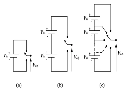
The schematics of single phase, single leg of inverters with different number of levels is shown in Fig. 1. The two-level inverter generates output of two voltage levels, whereas three-level inverter generates three voltage levels in output and so on. Therefore the MLIs are able to synthesize stepped voltage waveform and reduces harmonic content with higher number of levels.
Vo/p +
+
+
-Vdc
Vdc
Vdc +
-+
-Vdc
Vdc Vo/p
+
-Vdc
Vo/p
[image:1.595.324.544.241.396.2](a) (b) (c)
Fig. 1. Single-phase inverter configurations (a) two-level (b) three-level (c) n-level.
To control the output voltage of MLI various modulation techniques are used such as multicarrier PWM (MCPWM), Space vector PWM, Selective harmonic PWM [4-6]. Among the mentioned PWM techniques MCPWM is most commonly used method for switching of MLI because of its ease of applicability and implementation in various topologies. On the basis of carrier MCPWM can be classified as (i) phase shifted PWM (PS-PWM) and (ii) level shifted PWM (LS-PWM). The LS-PWM can be classified further into phase disposition (PD-PWM), phase disposition (PD-PWM), phase opposition and disposition PWM (POD-PWM), alternate phase opposition and disposition PWM (APOD-PWM), and inverted phase disposition (IPD-PWM)
© 2019, IRJET | Impact Factor value: 7.211 | ISO 9001:2008 Certified Journal | Page 3959 inverters multiple carriers are required, generating
switching pulses at different levels. In this case PWM pins and I/O registers of microcontroller is not sufficient at all as it is able to generates only single carrier wave that also lies on the reference line and cannot be shifted above or below the reference line. This paper brings concept of generation of MLI switching by SPWM technique using digital control of microcontrollers. Level shifted SPWM is applied because of its maximal harmonics cancellation property and ease of implementation.
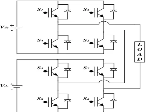
2. CASCADED H-BRIDGE CONFIGURATION
[image:2.595.305.563.114.342.2]The concept of CHB configuration is based on the series connection of H-bridge inverter to get stepped waveform with less harmonic contents. The sum of output voltages of each individual H-bridge unit will give total output voltage of the CHB inverter. The number of DC sources required in input of the CHB inverter is given by the expression (n-1)/2, total number of power semiconductor switches is given by 2(n-1), where ‘n’ is the number of voltage levels to be generated at the output. CHB inverter requires less number of power components as compared to other two conventional MLI topologies i.e. Diode Clamped MLI (DC-MLI) and Flying Capacitor MLI (FC-MLI), so that the circuitry is not so bulky and cumbersome. The single-phase configuration of five-level CHB is shown in Fig. 2., it is able to generate five-level of output voltage namely +2Vdc, +Vdc, 0, -Vdc, -2Vdc, shown by switching
state in Table I.
+
-S1
S2 S3
S4
+
-S5
S6 S7
S8
L O A D Vdc
Vdc
[image:2.595.304.563.120.325.2]
Fig. 2. Single-phase five-level CHB-inverter configuration with equal dc sources.
TABLE I. STATE OF THE INVERTER FOR FIVE-LEVEL OUTPUT VOLTAGE
3.
SINUSOIDAL PULSE WIDTH
MODULATION (SPWM) TECHNIQUE FOR
MULTILEVEL INVERTERS
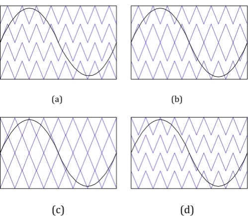
In multilevel SPWM number of carriers are required which makes it different from two level SPWM. For generation of ‘n’-number of levels of output, ‘n-1’ carriers are used and the interaction of the carriers with sinusoidal reference wave is used to generate pulsating signals for complementary switch pairs.
These multiple carriers can be used in horizontally shifted or vertically shifted manner. Horizontally shifted carrier SPWM technique gives advantage that each modules are shifted ON and OFF independently of amplitude of generated voltage, in constant number of periods. But the simplicity of implementation of vertically shifted carrier SPWM on any digital controller makes it more popular as compared to horizontally shifted carrier SPWM.
According to the placement of triangular carrier wave the vertically shifted SPWM can be further classified as follows:
When carriers are in same phase, phase disposition SPWM (PD-SPWM).
When carriers above the reference are in same phase and below the reference 180° out of phase from that of the above, phase opposition disposition (POD-SPWM).
Output
Voltage
S1 S2 S3 S4 S5 S6 S7 S8
+2Vdc 1 1 0 0 1 1 0 0
+Vdc 1 1 0 0 0 1 0 1
0 1 0 1 0 1 0 1 0
-Vdc 0 1 0 1 0 0 1 1
[image:2.595.44.279.538.719.2]© 2019, IRJET | Impact Factor value: 7.211 | ISO 9001:2008 Certified Journal | Page 3960 Carriers placed alternatively in opposition,
alternate phase opposition disposition (APOD-SPWM).
Carriers are oppositely placed as they are placed in PD-SPWM, inverted phase disposition (IPD-SPWM).
Among all the above mentioned techniques PD-SPWM gives less harmonics as compared to other SPWM techniques because it puts all harmonic energy directly into a common mode carrier components which cancelled in line-to-line output. All of the above mentioned scheme is shown in Fig. 3.
(a) (b)
[image:3.595.37.287.273.490.2](c) (d)
Fig. 3.Vertically shifted Multicarrier SPWM techniques (a) PD (b) POD (c) APOD (d) IPD.
4. Digital Implementation of SPWM
The SPWM technique can be implemented using microcontroller which is completely based on SPWM using sin reference and carrier reference waveform. But there is limitation of any microcontroller is that it can generate one carrier wave at a time which cannot be shifted to implement level shifted SPWM. Therefore in digital implementation samples of sinusoidal reference is taken at certain frequency. As the result sin waveform can be considered as sample and hold signal, which can be shifted according to level of output voltages have to be generated [7]. Accordingly the level shifted SPWM techniques can be implemented as follows.
Phase Disposition SPWM (PD-SPWM)
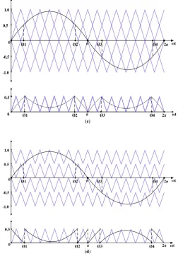
In PD-SPWM all the triangular carriers are aligned in same phase. Ø1, Ø2,Ø3,andØ4 are the four regions of comparisons to generate five-level of output voltage. In microcontroller the reference sin wave is fragmented in these four regions, which can be shifted below by amplitude of upper triangular wave in region Ø1 and Ø2. In the region between Ø3 andØ4 reference wave can be shifted above the reference by amplitude of lower two triangular wave. In such manner the reference sin is compared with single triangular carriers generated by the controller and get compared in same manner as it compare in conventional PD-SPWM. The implemented scheme is shown in Fig. 4(a).
Phase Opposition Disposition SPWM
(POD-SPWM)
In POD-SPWM carriers placed above the reference are in phase and carriers below the reference are 180° out of phase as that of the above reference. For the region 0 to π the sin reference is fragmented in same manner as that in PD-SPWM and get compared with carrier waves to give output of +Vdc and +2Vdc levels.
For the region π to 2π the sin wave is inverted this comparison gives output of -Vdc and then for the region
between Ø3 andØ4 sin wave is shifted down by the amplitude of the carrier wave to get compare with in order to generate -2Vdc level as shown in Fig. 4(b).
Alternate Phase Opposition Disposition
SPWM (APOD-SPWM)
In APOD-SPWM all the triangular carriers are aligned alternatively to each other. Here for the regions 0 to Ø1, Ø2 to π, and Ø3 to Ø4 the comparison of reference with carrier wave is same as that in PD-SPWM to synthesize +Vdc as well as -2Vdc level.
Whereas for the region Ø1 to Ø2, π to Ø3 and Ø4 to 2π the reference is inverted, and shifted accordingly to the level of output (+2Vdc and -Vdc) we have to generate.
The implementation of APOD-SPWM in microcontroller to produce five-level of voltage levels is shown in Fig. 4(c).
Inverted Phase Disposition SPWM
(IPD-SPWM)
© 2019, IRJET | Impact Factor value: 7.211 | ISO 9001:2008 Certified Journal | Page 3961 triangular wave with only base on the reference line
instead of tip of the wave on the line as it required for IPD. So that in order to implement the IPD-SPWM the sin wave generated digitally in microcontroller is inverted and get compared with triangular waveform as shown in Fig. 4(d). Here to generate the +Vdc level
the inverted sin wave in the region 0 to Ø1 and Ø2 to π is shifted above the reference line by an amplitude of the carrier wave and to get +2Vdc level in the region Ø1 to Ø2 the same sin wave is shifted above the reference by twice the amplitude of the carrier wave.
0 0.5 1.0
-0.5
-1.0
Ø1 Ø2 π Ø3 Ø4 2π ωt
ωt 0
0.5
Ø1 Ø2 π Ø3 Ø4 2π
(a)
0 0.5 1.0
-0.5
-1.0
Ø1 Ø2 π Ø3 Ø4 ωt
0 Ø1 Ø2 π Ø3 Ø4 2π ωt
0.5
(b)
0 0.5
1.0
-0.5
-1.0
Ø1 Ø2 π Ø3 Ø4 2π ωt
(c)
0 Ø1 Ø2 π Ø3 Ø4 2π ωt
0.5
0 0.5 1.0
-0.5
-1.0
Ø1 Ø2 π Ø3 Ø4 2π ωt
0 0.5
Ø1 Ø2 π Ø3 Ø4 2π ωt
[image:4.595.307.560.105.468.2](d)
Fig. 4. Five-level SPWM scheme Implemented in microcontroller (a) PD (b) POD (c) APOD (d) IPD.
5.Results and Observations
All the different types of level shifted SPWM techniques are used to generate the switching pulses of five-level CHB inverter. The proposed schemes are simulated in MATLAB/SIMULINK model, using two symmetrical dc sources of 115V each to synthesize five-level output voltage as shown in Fig. 5.
[image:4.595.305.563.634.741.2]© 2019, IRJET | Impact Factor value: 7.211 | ISO 9001:2008 Certified Journal | Page 3962 All of the mentioned SPWM techniques in the paper
is implemented using microcontroller dsPIC33EP256MC202 using generalized input-output ports and output compare module. The hardware prototype of five-level CHB is developed in laboratory and result for five-level output voltage is taken for input dc sources of 25V each with RL load of 100Ω, 1.5H for switching frequency of 2.1kHZ and the result is obtained by using digital storage oscilloscope (DSO) shown in Fig. 6.
Fig. 6. Five-level CHB-inverter output voltage and current (CH1=20 Volts/Div., time scale = 10ms)
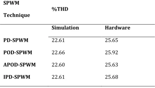
[image:5.595.36.289.258.385.2]Total Harmonic Distortion for both simulation and hardware results are analyzed for all the presented SPWM techniques and tabulated in Table. II.
TABLE II. COMPARISON OF DIFFERENT SPWMTECHNIQUES THD FOR MLI
SPWM
Technique %THD
Simulation Hardware
PD-SPWM 22.61 25.65
POD-SPWM 22.66 25.92
APOD-SPWM 22.60 25.63
IPD-SPWM 22.61 25.68
6.CONCLUSION
This paper brings successful implementation of multilevel multicarrier SPWM techniques by using single microcontroller instead of using master and slave controllers. Digital controllers are gaining more and more attention because of their ease of implementation, less complexity in circuitary as compare to analog circuit and less cost. Due to all such
advantages digital controls are becoming a better solution for industrial applications of power converters. In microcontroller based schemes the controller should be so dedicated that it can process for continuous sampling of the reference signal, it calculates exact crossings of carrier and reference signals, fragments the reference signals according to the level of generations. The proposed scheme of SPWM implementation gives same performance as that we get from natural SPWM. The validification of the scheme is shown by THD analysis of simulation and prototype results.
REFERENCES
[1] L. M. Tolbert, F. Z. Peng and T. G. Habetler. “Multilevel converters for large electric drives,” IEEE Trans. Ind. Applicat., vol. 35, no. 1, pp. 36-44, Jan./Feb. 1999.
[2] Kouro, S., Rebolledo, J., and Rodriguez, J.: ‘Reduced switching frequency modulation algorithm for high-power multilevel inverters’, IEEE Trans. Ind. Electron., 2007, 54, (5), pp. 2894–2901.
[3] Liu, Z.C., Kong, P.J., Wu, X.Z., and Huang, L.P.: ‘Implementation of DSP-based three-level inverter with dead time compensation’. IEEE Int. Power Electronics and Motion Control Conf., Xi’an, China, 2004, pp. 782–787.
[4] Liu, H. Hong, A. Q. Huang, "Real-time calculation of switching angles minimizing THD for multilevel inverters with step modulation," IEEE Trans . Industrial Electronics, vol. 56, no. 2, pp. 285-293, Feb. 2009.
[5] D. W. Kang, H. C. Kim, T. J. Kim, D. S. Hyun, "A simple method for acquiring the conducting angle in a multilevel cascaded inverter using step pulse waves,"IEEE Proceedings on Electric Power Applications, vol. 152, pp. 103-111, 2005.
[6] Kazuhiro Imaie, Osami Tsukamoto and Yoshiaki Nagai, “Control Strategies for Multiple Parallel Current-Source Converters of SMES System,” IEEE Transactions on Power Electronics, Volume 15, no.2, pp.377-385, 2000.
[7] M. A. Waghmare, P. A. Salodkar and H. Pillewan, “A single-phase multilevel inverter topology to synthesize multiple number of levels using common number of switches”, in Proc. Int. Conf. Power and
[image:5.595.34.289.495.639.2]