FALAHI, GHAZAL. Design, Modeling and Control of Modular Multilevel Converter based HVDC Systems. (Under the direction of Dr. Alex Q. Huang.)
Modular multilevel converter (MMC) is a relatively new and promising topology, which has gained a lot of interest in industry in the recent years due to its modular design and easy adaption for applications that require different power and voltage level, such as power transmission through HVDC. This dissertation aims to investigate the operation of MMC based HVDC systems and propose solutions to improve the performance of the system by using new devices and improving the control strategies.
First, detailed design of MMC-HVDC system and its parameters are presented. Then common modulation techniques used for multilevel converters are reviewed and a real-time nearest level modulation with capacitor voltage balancing and minimization of circulating current is proposed. The concept of ETO thyristor based MMC is proposed for HVDC systems and power stage losses are analyzed and calculated from conventional loss calculation techniques for an IGBT and ETO based MMC.
controller is eliminating negative and zero sequence currents and to improve the overall performance. The controller calculates zero and negative sequence reference voltages and eliminates zero and negative sequence currents without using any current regulator. Therefore the controller is very fast and robust.
Fourth, modular multilevel converter (MMC) based HVDC system is also evaluated during voltage dips and a new control strategy with LVRT capability is proposed for MMC based HVDC systems to improve the performance. The algorithm controls the system to generate the required active and reactive powers that are calculated mathematically based on the ratings of the HVDC-MMC system and LVRT requirements. The injected active and reactive power values obey the LVRT curve besides the method is adaptable to different grid codes. The mathematical calculations are presented and EMTDC/PSCAD simulation proves the performance of the proposed controllers. Performance of the modeled MMC-HVDC system is also analyzed in detail during DC short circuit faults.
Last, the new concept of MMC with unequal DC values is proposed. The common modulation techniques used for MMC are reviewed and use of minimal THD modulation for MMC is proposed. The real-time performance of minimal THD modulation with MMC is evaluated with both RTDS and PSCAD.
by Ghazal Falahi
A dissertation submitted to the Graduate Faculty of North Carolina State University
in partial fulfillment of the requirements for the degree of
Doctor of Philosophy
Electrical Engineering
Raleigh, North Carolina
2015
APPROVED BY:
_______________________________ ____________________________________ Dr. Alex Q. Huang Dr. Subhashish Bhattacharya
DEDICATION To my parents
BIOGRAPHY
ACKNOWLEDGMENTS
First, I would like to express my sincere appreciation to my advisor, Dr. Alex Huang for his continuous support and encouragement. Dr. Huang’s broad vision, deep knowledge and wise direction have helped me a lot in my research at NC State towards completion of this dissertation.
I am also very grateful to my committee members Dr. Subhashish Bhattacharya, Dr. Srdjan Lukic and Dr. Xiangwu Zhang for their valuable comments and helps. It has been a pleasure to work at FREEDM Systems Center and it provided me the opportunity to collaborate with so many knowledgeable people. My sincere gratitude goes to FREEDM family for providing such a friendly and pleasant atmosphere. I appreciate the assistance from the staff members of FREEDM Systems Center including Mr. Rogelio Sullivan, Ms. Karen Autry, Ms. Colleen Reid, Ms. Audrey Callahan, Mr. Hulgize Kassa and Mr. Gregory Norris.
My deepest appreciation goes to my parents and family, Mehri Abdolahi, Naser Falahi, Milad Falahi and Misagh Falahi who have always supported me during my studies.
TABLE OF CONTENTS
LIST OF TABLES ... ix
LIST OF FIGURES ...x
INTRODUCTION ...1
1.1 State of the Art ... 4
1.2 Contributions... 9
1.3 Organization ... 10
MODULAR MULTILEVEL CONVERTER BASED HVDC SYSTEM DESIGN ...13
2.1 Introduction ... 13
2.2 MMC mathematical model and operation principal ... 13
2.3 MMC design for HVDC application... 19
Choosing required number of sub-modules ... 21
Sub-module capacitor dimensioning... 22
Arm inductor design ... 24
2.4 Semiconductor devices for HVDC systems ... 28
Gate turn off thyristor (GTO) ... 29
IGCT ... 29
IGBT ... 30
Emitter Turn-off (ETO) Thyristor ... 31
2.5 Design of MMC based on ETO thyristor ... 33
Effect of clamp inductor on MMC circulating current ... 36
MMC MODULATION TECHNIQUES ...38
3.1 Introduction ... 38
3.2 Modulation techniques ... 38
3.3 Carrier based modulation techniques ... 39
Sinusoidal PWM (SPWM) ... 40
3.3.1.1 Level shifted or phase disposition PWM ... 41
3.3.1.2 Phase shifted PWM ... 43
3.4 Space vector modulation (SVM) ... 45
3.5 Selective Harmonic Elimination PWM ... 47
3.6 Nearest level modulation (NLM) ... 48
3.7 Proposed real time nearest level modulation (NLM) with capacitor voltage balancing ... 50
3.8 Loss calculation ... 53
Voltage source converter value power losses ... 53
Conventional conduction loss calculation for MMC ... 59
Conventional switching loss calculation ... 67
3.10 Design and loss calculation of ETO based MMC ... 69
Analytical power loss calculation of ETO based MMC ... 69
3.11 Proposed loss calculation under proposed modulation scheme ... 73
Cooling system design and thermal analysis ... 88
Cooling System Design... 91
MMC-HVDC SYSTEM CONTROL AND POWER FLOW ANALYSIS ...93
4.1 Introduction ... 93
4.2 MMC-HVDC mathematical equations ... 94
4.3 Current Control in HVDC-MMC system ... 96
4.4 Active and reactive power reversal ... 101
4.5 DC link voltage control ... 102
4.6 AC voltage control ... 104
4.7 Power equations ... 106
Maximum power transfer ... 109
...110
5.1 Introduction ... 110
5.2 MMC generalized mathematical model ... 110
5.3 Symmetrical components ... 113
5.4 MMC instantaneous real and reactive power equations ... 115
5.5 AC Fault propagation in transformer-less HVDC-MMC system ... 116
Single line to ground fault... 117
Three-phase fault ... 122
5.5.2.1 50% voltage sag on both rectifier and inverter sides ... 126
5.6 Performance improvement of MMC-HVDC system during fault and unbalance condition ... 126
Negative sequence ... 127
Zero sequence ... 128
Proposed control structure ... 129
Low voltage and fault ride through control of HVDC-MMC... 137
5.7 Proposed LVRT control structure ... 141
5.8 MMC operation and protection under DC link short circuit fault ... 149
MMC WITH UNEQUAL DC VALUES ...162
6.1 Introduction ... 162
6.2 Structure of MMC with unequal DC values ... 163
6.3 Minimal THD modulation ... 164
6.4 Performance of the proposed modulation technique ... 168
6.5 Loss calculations of the proposed MMC structure ... 174
LIST OF TABLES
Table 1-1. MMC for HVDC projects. ... 3
Table 1-2. Multilevel converter pros and cons. ... 7
Table 1-3. HB MMC pros and cons. ... 7
Table 1-4. Full-bridge based MMC pros and cons. ... 8
Table 2-1 Switching state of sub-modules. ... 15
Table 2-2 MMC specifications in HVDC system ... 20
Table 2-3 Comparison of high power devices [35] ... 33
Table 3-1 MMC-HVDC system specifications... 60
Table 3-2 Switching state of semiconductor based on direction of current flow ... 61
Table 3-3 IGBT CM1500HG-66R parameters ... 65
Table 3-4 ABB fast recovery diode 5SDF 16L4503 ... 66
Table 3-5 Conduction of devices in MMC ... 81
Table 3-6 Individual averaged device losses for MMC sub-modules ... 87
Table 3-7 Device junction temperature, P=500MW operation ... 91
Table 3-8 Device junction temperature, P=1000MW operation ... 91
Table 4-1 HVDC-MMC system specifications... 98
Table 6-1 Comparison of some well-known low switching frequency modulation techniques ... 166
Table 6-2 Sub-modules duty cycle ... 174
LIST OF FIGURES
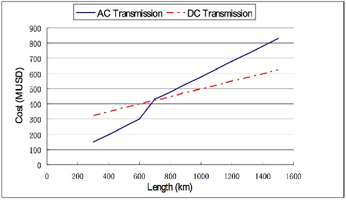
Figure 1-1. Cost comparisons of HVDC and HVAC systems by length (2000MW). ... 1
Figure 1-2. Typical MMC tower of a phase based on IGBT proposed by Siemens (left) Layout of MMC-HVDC substation proposed by Siemens (right) ... 4
Figure 2-1. Half bridge sub-modules of MMC. ... 14
Figure 2-2. Switching state of sub-modules. ... 15
Figure 2-3. Modular multilevel converter. ... 17
Figure 2-4. Total DC voltage controller (left), individual capacitor voltage controller (right) ... 18
Figure 2-5. Power controller (left), current and voltage abc to dq transformations ... 19
Figure 2-6. Modulation reference generation of upper and lower arms ... 19
Figure 2-7. Sub-module capacitor voltages (zoomed) ... 23
Figure 2-8. Sub-module capacitor voltages ... 23
Figure 2-9. Peak circulating current versus inductor value. ... 27
Figure 2-10. Circulating current. ... 27
Figure 2-11. Development time line of high power semiconductor devices [30] ... 28
Figure 2-12. Power devices used for HVDC systems ... 30
Figure 2-13. Cross section of ETO ... 32
Figure 2-14. Gen-4 ETO thyristor at 4.5kV/4kA (a) photo (b) simplified equivalent circuit 32 Figure 2-15. MMC structure with ETO thyristor based sub-modules ... 35
Figure 2-16. ETO based Sub-module (a) when the clamp diode is on (b) when diode is off 37 Figure 2-17. Circulating current of conventional and proposed ETO based MMC-HVDC ... 37
Figure 3-1. Classification of multilevel modulation methods ... 40
Figure 3-2. Phase disposition SPWM ... 41
Figure 3-3. Phase shifted SPWM ... 43
Figure 3-4. Comparison of two common phase shifted PWM techniques ... 44
Figure 3-8. Real-time NLM with capacitor voltage balancing ... 52
Figure 3-9. Sub-module capacitor voltages with proposed real-time NLM ... 52
Figure 3-10. Sub-module capacitor voltages with proposed real-time NLM (zoomed) ... 53
Figure 3-11. Typical IGBT and diode on-state characteristics: real (left) and piecewise-linear approximation (right) ... 56
Figure 3-12. Typical IGBT and diode switching energies ... 58
Figure 3-13. Upper arm current in one phase ... 60
Figure 3-14. Typical sub-module utilization curve over a cycle[47]... 62
Figure 3-15. Semiconductor loss break down of MMC-HVDC with IGBT ... 68
Figure 3-16. Test curve of Gen-4 ETO power loss characteristics at junction temperature of 125°C, on-state voltage (lest picture), turn-off energy per pulse at 2.5kV DC bus voltage (right picture) ... 70
Figure 3-17. Semiconductor loss break down of MMC-HVDC with ETO ... 72
Figure 3-18. Generated and reference arm voltage ... 74
Figure 3-19. Reference arm voltage and current (PF=1) ... 76
Figure 3-20. Reference arm voltage and current (PF=+0.95) ... 77
Figure 3-21. Reference arm voltage and current (PF=-0.95) ... 77
Figure 3-22. Reference arm voltage and current (PF=0) ... 78
Figure 3-23. Reference arm voltage and current ... 79
Figure 3-24. Device operation in MMC ... 80
Figure 3-25. Real time loss calculation for 8 sub-modules in each arm ... 82
Figure 3-26. Sub-module device losses (Watts), different operating conditions (averaged over 200 cycles) ... 83
Figure 3-27. Proposed modulation and loss calculation diagram ... 84
Figure 3-28. S11 power losses ... 84
Figure 3-29. S12 power losses ... 85
Figure 3-30. S13 power losses ... 85
Figure 3-31. S14 power losses ... 85
Figure 3-32. S15 power losses ... 86
Figure 3-34. S17 power losses ... 86
Figure 3-35. S18 power losses ... 87
Figure 3-36. Half-Bridge MMC sub-module with ETO devices ... 89
Figure 3-37. Two different structure for component arrangement of ETO HB blocks ... 89
Figure 3-38. Physical arrangement of the stack in modular half-bridge showing three heat pipes showing heat flow into heat pipes from ETO and diodes ... 90
Figure 3-39. Heat pipe cooling ... 90
Figure 3-40. Operation mechanism of a typical heat-pipe ... 92
Figure 4-1. MMC-HVDC system single line diagram... 96
Figure 4-2. Current control ... 97
Figure 4-3. System response to step change in active power (0.8 to 1.2 pu) active and reactive powers respectively ... 99
Figure 4-4. System response to step change in reactive power (0.2 to 0.4pu) reactive and active powers respectively ... 100
Figure 4-5. Dynamic response of the system to active and reactive power reversal ... 101
Figure 4-6. DC voltage control ... 102
Figure 4-7. Dynamic response of the system to step change in Vdc ... 103
Figure 4-8. Dynamic response of system to change in AC voltage ... 105
Figure 4-9. Equivalent circuit and phasor diagram of HVDC system ... 106
Figure 5-1. Modular multilevel converter circuit configuration ... 113
Figure 5-2. Fault on the AC line ... 116
Figure 5-3. Dynamic performance of HVDC-MMC during SLG fault at inverter side, 3phase currents, DC link voltage, Negative sequence voltages at PCC2, zero sequence voltages at PCC2, zero sequence current at PCC2 respectively... 119
Figure 5-4. Dynamic performance of HVDC-MMC during SLG fault at rectifier side, 3phase currents, active power of both sides, DC link voltage respectively ... 121
Figure 5-5. Dynamic response of the system to three-phase fault at rectifier side ... 123
Figure 5-9. Zero sequence voltages and currents at PCC when SLG is applied to side 2 .... 129
Figure 5-10. Zero and negative sequence calculation ... 130
Figure 5-11. Proposed control structure... 131
Figure 5-12. Dynamic performance of MMC-HVDC system with proposed control structure SLG fault applied at 0.3 sec ... 133
Figure 5-13. Zero sequence and negative sequence voltages ... 134
Figure 5-14. Circulating current fault at t=0.3, conventional controller ... 135
Figure 5-15. Circulating current fault at t=0.3, proposed controller ... 135
Figure 5-16. Sub-module capacitor voltages, fault at t=0.3, conventional controller ... 135
Figure 5-17. Sub-module capacitor voltages, fault at t=0.3, proposed controller ... 136
Figure 5-18. System response to fault with proposed controller ... 137
Figure 5-19. Typical investment cost for an AC line and a DC line ... 139
Figure 5-20. Power controller with LVRT capability ... 143
Figure 5-21. Low voltage ride through curve ... 145
Figure 5-22. The required percentage of reactive current during LVRT ... 145
Figure 5-23. Dynamic response of the HVDC-MMC system to low voltage ride through profile ... 146
Figure 5-24. System voltages, currents and DC link voltage with typical control, voltage sag applied at t=0.3 sec ... 147
Figure 5-25. System reactive power, currents, DC link voltage and active power with LVRT control, voltage sag applied at t=0.3 sec ... 148
Figure 5-26. Possible paths of short circuit current injection from the grid to MMC ... 150
Figure 5-27. Equivalent circuit in stage 1 ... 151
Figure 5-28. Simplified equivalent circuit of MMC-HVDC during DC short circuit fault (stage 1) ... 152
Figure 5-29. DC current and DC link voltage when the short circuit fault is applied at 0.2 secs ... 154
Figure 5-30. Equivalent circuit during stage 2... 155
Figure 5-31. Equivalent circuit during stage 3... 156
Figure 5-32. MMC-HVDC operation during DC short circuit fault ... 157
Figure 5-34. DC link voltage after DC short circuit fault is applied at t=0.2 secs ... 158
Figure 5-35. DC current, DC short circuit fault is applied at t=0.2 secs ... 159
Figure 5-36. MMC arm current, DC short circuit fault is applied at t=0.2 secs ... 160
Figure 5-37. DC link voltage, DC short circuit fault is applied at t=0.2 secs ... 160
Figure 5-38. AC currents inverter side, DC short circuit fault is applied at t=0.2 secs ... 161
Figure 5-39. AC currents rectifier side, DC short circuit fault is applied at t=0.2 secs ... 161
Figure 6-1. Modular multilevel converter with unequal DC values, one phase ... 164
Figure 6-2. Multilevel inverter Phase Voltage with with staircase modulation ... 166
Figure 6-3. Minimal THD algorithm flowchart ... 167
Figure 6-4. Overall structure of the converter and modulation technique ... 170
Figure 6-5. Output voltage, MMC, minimal THD modulation ... 171
Figure 6-6. Output voltage of MMC, PS-PWM ... 171
Figure 6-7. Output voltage of MMC with unequal dc sources using minimal THD modulation ... 171
Figure 6-8. MMC, Vo harmonic spectrum, minimal THD modulation... 172
Figure 6-9. MMC Vo harmonic spectrum CS-PWM... 172
Figure 6-10. MMC with unequal DC and minimal THD modulation, Vo harmonic spectrum ... 173
INTRODUCTION
High Voltage Direct Current (HVDC) is a technology that transmits power in forms of DC to increase the efficiency of bulk power transmission over long distances. HVDC systems have a sending and a receiving station and they convert electricity from AC to DC at the sending station and then back to AC at the receiving station. They also allow electricity to flow in both directions so demand and supply are matched more effectively. HVDC systems are also used to connect incompatible AC networks and improve their efficiency and stability. Figure 1-1 shows the cost comparison of HVDC and HVAC systems by length [1].
First HVDC systems were based on line-commutated converters (LCC), which could transfer large amount of power but they had low controllability and large harmonic content. With development of power electronic devices, voltage source converters (VSC) are more accepted in high voltage applications. VSC based HVDC is a relatively new type of transmission system incorporating controllable switching converters which does not have the drawbacks of conventional LCC based HVDC systems. VSC based HVDC systems can control active and reactive power independently therefore they improve power transfer capability and network stability. They can also be used to start up weak AC networks that lack generation and they do not require a minimum power level that can be transferred hence the power can be controlled between 0 and 100%. The VSC-HVDC systems are usually operated at higher switching frequencies compared to classic HVDC systems therefore the size of required AC filters are smaller [2].
Table 1-1. MMC for HVDC projects.
Project Installed year Manufacturer DC link Voltage Power (MW)
Trans Bay 2010 Siemens ±200 KV 400
BorWin1 2013 Siemens 300 KV 800
Helwin1 2013 Siemens 259 KV 576
DolWin1 2013 ABB ±320 KV 800
SylWin1 2014 Siemens ±320 KV 864
South-west link 2014 Alstom N/A 1440
HelWin2 2015 Siemens ±320 KV 690
Dolwin2 2015 ABB ±320 KV 900
the converter is high which results in low harmonic distortion. Another advantage of
MMC-HVDC compared to classic VSC-MMC-HVDC is that the 𝑑𝑣𝑑𝑡 is reduced, as the voltage steps at AC
terminals are smaller.
Figure 1-2. Typical MMC tower of a phase based on IGBT proposed by Siemens (left) Layout of MMC-HVDC substation proposed by Siemens (right)
and is a suitable candidate for VSC based HVDC. A lot of research and publications are published to analyze different aspect of operation and control of MMC or MMC based transmission systems. Due to its modular structure MMC is a very robust suitable converter for transmission and high voltage applications [6].
One of the drawback of MMC topology is circulating current that causes power losses and increases stress on the devices. Circulating current has been studied in a lot of publications and several method have been proposed to minimize circulating current in converter’s phase leg [7, 8]. Another issue of MMC is the capacitor voltage balancing that plays an important role in stable operation of the system and minimizing the circulating current. Several control strategies are proposed to improve the equal voltage sharing among sub-module capacitors [9-11].
Dr. Akagi presented a detailed review of MMC converter and a comprehensive control strategy to operate MMC in a paper, which is still the base of so many research publications on MMC. The controller includes four main parts to regulate the sub-module capacitor voltages, active and reactive currents and to balance the sub-module capacitor voltage in a phase leg [12].
wind farms will be commissioned in the next few years. Main technical and economic aspects of development of multilevel converters are [13]:
1) Modular realization:
Scalable to different power- and voltage levels
Insensitive to variable semiconductor parameters
2) Multi-level waveform:
Expandable to any number of voltage steps
Low total harmonic distortion
Dynamic sharing of the power devices
3) High availability:
Use of approved semiconductor devices
Redundant operation
4) Failure management:
Fail safe operation in device failures
Avoidance of mechanical damage (high magnetic forces caused by surge currents)
5) Investment and life cycle cost:
Modular structure
Table 1-2. Multilevel converter pros and cons.
Multilevel converter advantages Multilevel converter disadvantages
Low switching loss More complex control algorithm
Easily scalable to high voltages High number of semiconductors
Virtually no harmonics Less compact
Table 1-2 summarizes the multilevel converter advantages and disadvantages. The MMC based on half bridge (HB) cells has lowest component count compared to other multilevel converter topologies used for HVDC application however it has the possibility of one output voltage polarity. Table 1-3 shows the HB based MMC pros and cons.
Table 1-3. HB MMC pros and cons.
HB MMC advantage HB MMC disadvantages
Lowest component count No capability of suppressing DC side
faults, AC breaker must be tripped
or a hybrid structure is used to optimize the design. Table 1-4 summarizes the Full-Bridge based MMC pros and cons.
Recently, a lot of publications and research projects evaluated MMC control and performance [4, 13-16]. There are some papers reviewing modulation techniques used for MMC and some papers proposed unconventional modulation techniques such as selective harmonic elimination (SHE) to improve the performance of MMC [17]. Besides several researches focused on the performance of MMC in HVDC applications under different operating conditions and faults.
Dynamic performance of HVDC-MMC system under fault or unbalance condition has been analyzed briefly in a few publications. During unbalance operation there are zero and negative sequence terms in system voltages and currents. A current regulator based control to eliminate zero and negative sequence components is proposed in [18] which uses additional control loops to eliminate undesired components and adds to complexity of MMC control.
Table 1-4. Full-bridge based MMC pros and cons.
Full-bridge MMC advantage Full-bridge MMC disadvantages
Output voltage can be either polarity High loss due to twice number of
Growing number of MMC installations for high voltage applications show the success and market acceptance of MMC topology. There is still small number of publications focusing on performance improvement of MMC-HVDC systems under fault and unbalance conditions [15]. Fast penetration of MMC in high voltage applications demands more research on the performance of this converter and detail study of the operation and control system.
1.2 Contributions
The power stage design, modulation and control of MMC-HVDC system can be modified to optimize the cost and performance of system. This study focuses on comprehensive modeling, control and performance improvement of MMC-HVDC systems. The main contributions of this research include:
1) Design a complete modular multilevel converter based HVDC system using ETO thyristors.
2) Propose a real-time low frequency modulation with monitoring and balancing of sub-module capacitor voltages and minimizing circulating current.
3) Propose a loss calculation technique based on detailed analytical loss equations for the proposed 60Hz modulation to find the accurate individual device losses.
5) Propose a new control techniques to improve MMC-HVDC system reliability during voltage sags and faults.
6) Propose a new MMC configuration to improve harmonic performance and to incorporate minimal THD modulation technique with the proposed MMC configuration to obtain a better output voltage quality.
1.3 Organization
Followed by state of the art presented in this chapter, chapter 2 provides the structure of modular multilevel converter based HVDC systems. It starts by reviewing the mathematical model of MMC and design of MMC for HVDC systems. Then a brief over view of the devices used in high voltage controlled converters is provided and ETO thyristor is introduced as a good candidate for HVDC application.
MMC structure based on ETO thyristors is presented and the sub-modules and passive components are designed. The effect of ETO thyristor sub-module design with clamp on the performance of MMC is evaluated and it is shown that the clamp inductor helps in reducing the circulating current. The last section in chapter explains the conventional control of MMC and its structure.
selective harmonic elimination and nearest level modulation and proposes a real-time nearest level modulation based technique for the designed MMC-HVDC system.
Operation of sub-modules and power stage losses are then analyzed and a detailed real-time loss calculation technique is proposed to calculate the accurate individual device losses during the operation. Finally a cooling system is design for the ETO thyristor based sub-modules and simulation of the device junction temperature is presented.
Chapter 4 presents the MMC-HVDC system layout, control and operation. The mathematical equations of the system and operation under normal condition is shown and different controllers in the HVDC system and their operation are explained. Active and reactive power flow in the system and conditions for maximum power transfer are demonstrated.
Chapter 5 reviews the MMC-HVDC system operation during faults. The first parts show the mathematical equations and performance under AC fault or unbalance operating condition. Later a controller is proposed to improve the MMC-HVDC system performance under unbalance condition. The structure of the proposed controller and its operation is presented and PSCAD simulation results prove the effectiveness of the proposed solution. A low voltage ride through controller (LVRT) is also proposed for the MMC-HVDC system to improve the reliability of the system under voltage sags and faults and the simulation results to show the performance of LVRT controller are presented. Last section of this chapter reviews the operation of simulated system under DC link short circuit faults.
and has lower THD compared to conventional structure. Minimal THD modulation is used to operate this configuration and output voltages are compared using different modulation techniques. Controller hardware in the loop is performed for the proposed structure to prove lower THD in the output voltage compared to conventional configuration. Losses are calculated for MMC with unequal DC values and compared to conventional MMC.
MODULAR
MULTILEVEL
CONVERTER
BASED HVDC SYSTEM DESIGN
2.1 Introduction
Modular multilevel converter (MMC) is an emerging multilevel converter topology introduced in 2001 and it is highly appealing for high voltage applications such as HVDC. MMC achieves high number of voltage levels by connecting several identical power electronic building blocks called sub-modules in series and it has the lowest semiconductor count comparing to other multilevel converters[19]. Modular structure of MMC allows adding modules to the design, which provides redundancy and increases the reliability of the entire system. Several modulation techniques are used for MMC and for high voltage applications with large number of sub-modules switching frequency can be as low as fundamental frequency which greatly reduces the losses.
2.2 MMC mathematical model and operation principal
with an arm inductor. The total DC voltage of each MMC arm equals the total DC link voltage and each sub-module in the arm will provide Udc/n if there are n sub-modules in the arm.
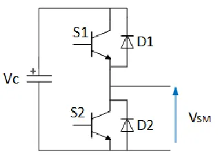
Figure 2-1. Half bridge sub-modules of MMC.
Sub-modules are inserted or bypassed based on the switching state of two switching devices in each half bridge; two switches are complementary. Table 2-1 depicts the sub-module output voltage in different switching states [20]. The switching state of each device depends on the direction of the arm current and reference modulation waveform. When upper switch or diode (S1 or D1) conduct the sub-module capacitor is inserted in the arm and conduction of the
lower devices (S2 or D2) results in bypassing the sub-module capacitor. Once a sub-module is
Table 2-1 Switching state of sub-modules.
State S1 S2 D1 D2 Vsm
1 ON OFF OFF OFF Vc
2 OFF ON OFF OFF 0
3 OFF OFF ON OFF Vc
4 OFF OFF OFF ON 0
Figure 2-2. Switching state of sub-modules.
D1
D2
S1
S2
ipa Vc
D1
D2
S1
S2
ipa
Vc
D1
D2 S1
S2
ipa
Vc
D1
D2 S1
S2
The currents in phase-k (k=a, b, c) consist of ik-up and ik-lowwhich are the upper and
lower arm current in each phase. Applying KVL to the arms of the converter yields to the following:
𝑢𝑘− (𝑢0+𝑈2𝑑𝑐− 𝑢𝑘−𝑢𝑝) = 2𝐿𝑑𝑖𝑘−𝑢𝑝𝑑𝑡 (2.1)
𝑢𝑘− (𝑢0+𝑈𝑑𝑐
2 + 𝑢𝑘−𝑙𝑜𝑤) = 2𝐿 𝑑𝑖𝑘−𝑙𝑜𝑤
𝑑𝑡 (2.2)
𝑢𝑘− (𝑢0+𝑈𝑘−𝑙𝑜𝑤2−𝑈𝑘−𝑢𝑝) = 𝐿𝑑𝑖𝑑𝑡𝑘 (2.3)
𝑖𝑘1+ 𝑖𝑘2 = 𝑖𝑘 (2.4)
𝑖𝑐𝑖𝑟𝑐 =𝑖𝑢𝑝𝑝𝑒𝑟+𝑖𝑙𝑜𝑤𝑒𝑟
2 (2.5)
Where uk is the phase k voltage, u0 is the potential to ground DC side neutral point and
the inductance of each arm equals 2L. The circulating current is the difference between the upper arm current (ik_up) and lower arm current (ik_low). This current flows through the DC
source to the phase leg for the single-phase configuration and it flows through different phase legs in three-phase configuration [21-24].
The MMC grid connection dynamic is described in (2.6).
𝑢𝑘− (𝑣𝑘+ 𝑢0) = 𝐿𝑘𝑑𝑖𝑑𝑡𝑘+ 𝑅𝑘𝑖𝑘 (2.6)
Control system for the each MMC converter includes four parts [12]:
2) The averaging controller that controls the total capacitor voltages in each leg to follow the reference value which is 2Vdc and minimize the circulating current.
3) The system controller, which controls active and reactive power. The reference of active power is determined by network demanded active power or the DC-link voltage controller. The reference for reactive power is either determined by ac voltage regulator or by the reactive power demand.
Figure 2-3. Modular multilevel converter.
Cell 2 Cell n Cell (n+1) Cell (n+2) Cell 1 Cell (2n) DC link va vb vc DC link u0 ia-up ia-low Udc/2
Udc/2
ia ib ic 2L 2L 2L 2L 2L 2L La Lb Lc
ib-up ic-up
ib-low ic-low
4) The PWM voltage command generation, which adds up the output of three mentioned controllers to build the modulation waveform. The overall control structure is shown in Figure 2-4 and Figure 2-5. The ac voltage command or modulation index for each phase is calculated by adding the output of three mentioned controllers as shown in the following equations.
𝑉𝑗𝑢∗ = 𝑉𝐴𝑢∗ + 𝑉𝐵𝑗𝑢∗ −𝑣𝑢
∗
4 +
𝐸
8 (j:1-n) (2.7)
𝑉𝑗𝑢∗ = 𝑉𝐴𝑢∗ + 𝑉𝐵𝑗𝑢∗ +𝑣𝑢
∗
4 +
𝐸
8 (j: n+1 - 2n) (2.8)
The voltage command is normalized by each dc-capacitor voltage Vcju and compared with a
triangular waveform having a maximum value of unity and minimum value of zero with a carrier frequency of fc. Phase shifted PWM modulation technique is used for switching and
carrier waveform of each cell is phase shifted by 360/n [12].
PI PI
1/2 Vc*
Vcu
Ik-low
Ik-up
Icir*
Icir
VAu*
Total DC voltage controller
PI Vc*
Vcju (j=1-2n)
±
-1 :-Ik-up , Ik-low ≥ 0
+1 :-Ik-up , Ik-low ≤ 0 VBju*
Figure 2-5. Power controller (left), current and voltage abc to dq transformations
Figure 2-6. Modulation reference generation of upper and lower arms
2.3 MMC design for HVDC application
In this section MMC is designed for an HVDC system with specifications presented in Table 2.2. The next section cover overall system structure and passive components design.
Vmk(k=a,b,c)
PI
i*dref
Vod
iod
PI
i*qref
ω0Leq
ω0Leq
ioq
Voq
3
dq/abc
System controller
Abc/dq 3 Voj
ω0
Abc/dq
3 ioj
ω0
iodq
vodq
VAu*
VBju* Vi/n E/(2n)
Vju* (j=1-n)
dAneg
VAu*
VBju* Vi/n E/(2n)
Vju* (j=n+1-2n)
Table 2-2 MMC specifications in HVDC system
The based values for the modeled MMC-HVDC system are calculated in (2.9)-(2.16).
𝑆𝑏𝑎𝑠𝑒 = √3𝑉𝐿𝐿−𝑏𝑎𝑠𝑒𝐼𝐿𝑏𝑎𝑠𝑒 ≈ 500𝑀𝑊 (2.9)
𝑉𝑏𝑎𝑠𝑒 =√2×138𝑘𝑣√3 = 112.67𝑘𝑣 (2.10)
𝐼𝑏𝑎𝑠𝑒= 2116𝐴 (2.11)
𝑍𝑏𝑎𝑠𝑒 =𝑉𝐿𝐿−𝑏𝑎𝑠𝑒𝐼
𝑏𝑎𝑠𝑒 = 65.19 (2.12)
𝐿𝑏𝑎𝑠𝑒 = 𝑍𝑏𝑎𝑠𝑒
𝜔𝑏𝑎𝑠𝑒 = 0.173𝐻 (2.13)
𝐶𝑏𝑎𝑠𝑒= 𝜔𝑏𝑎𝑠𝑒
𝑍𝑏𝑎𝑠𝑒 = 5.78𝐹 (2.14)
System parameters Values
AC system 138 kV-LL rms
Power 500 MW
Fundamental frequency 60Hz
MMC switching frequency 60Hz
Ls 5mH
DC link cable specifications Length 200 km
Resistance 0.01 Ω/km
Inductance 1.0 mH/km
Choosing required number of sub-modules
Manufacturers usually build modules therefore the capacitor value and sub-module voltages are some fixed numbers. The power and DC voltage for specific HVDC application are also fixed values. The number of required sub-modules is calculated based on the voltage withstand capability of sub-modules and HVDC system’s power and DC link voltage. The power and DC link voltage of HVDC define the first constraint for choosing number of sub-modules.
𝑁 ≤ 𝑃𝑠
3.𝐾.𝜔0.𝜀.𝑉𝑐2.𝐶𝑆𝑀[1 − (
𝑘.𝑐𝑜𝑠𝜑
2 )
2]
3 2
(2.17)
The second constraint is defined by the voltage withstand capability of sub-module capacitors, the number of sub-modules should be selected such that the voltage share of each sub-module is smaller than the maximum withstand capability of sub-module.
𝑁 ≥ 𝑉𝑑𝑐
𝑉𝑐𝑚𝑎𝑥 (2.18)
Sub-module capacitor dimensioning
In high power applications incorporating MMC with high number of sub-modules, such as HVDC systems, the sub-module capacitor is an important parameter to design and optimizing the capacitance is critical. Since there is no DC link capacitor in MMC and the sub-module capacitors are the only energy source, they should be able to provide energy for at least one cycle in case of DC link failure. When the sub-module capacitors are inserted in the arm of the converter, the arm current passes through the capacitor causing the capacitor voltage fluctuations. One criterion in selecting sub-module capacitors is to suppress these voltage fluctuations to a pre-defined value to meet required specifications. In modular multilevel converter sub-module capacitor voltages are not the same and this fact causes problem in applications such as HVDC where the switching frequency is relatively low. Therefore a sub-module capacitor balancing technique is usually added to the modulation technique to keep the capacitor voltages balanced. Some publications find the error value in the arm voltage caused by unbalance capacitor voltages and design the capacitors to minimize the error [25-27].
𝐶𝑆𝑀 = 𝑃𝑠
3.𝐾.𝑁.𝜔0.𝜀.𝑉𝑐2[1 − (
𝑘.𝑐𝑜𝑠𝜑 2 ) 2] 3 2 (2.19)
Where CSM is the sub-module capacitor, Ps is the three phase apparent power, K is the
voltage modulation index, cosφ is the power factor, N is the number of sub-modules, ω0 is the
fundamental frequency, VC is the mean value of sub-module voltages and ε is the sub-module
voltage ripple. VC equals Vdc/N and the controls system aims at keeping VC constant. The
sub-module capacitor is calculated to be CSM=2.5mF.
Figure 2-7. Sub-module capacitor voltages (zoomed)
0.5 0.52 0.54 0.56 0.58 0.6 0.62 0.64 0.66 0.68 0.7
0.35 0.36 0.37 0.38 0.39 0.4 time (secs) Submodul e capacit or vol tages( pu)
0 0.5 1 1.5 2 2.5
Arm inductor design
A significant feature of MMC is the presence of the arm inductance. The arm inductance compensates the difference between the phase-leg and DC side voltage therefore it impacts the circulating current. Dominant term in circulating current is second harmonic therefore arm inductance can be chosen to minimize this term in the circulating current. Equations (2.20) and (2.21) show the reference upper and lower arm voltages.
𝑢𝑢𝑝𝑟𝑒𝑓= 𝑈2𝑑𝑐− 𝑒̂𝑣cos (𝜔𝑡) (2.20)
𝑢𝑙𝑜𝑤𝑟𝑒𝑓 = 𝑈2𝑑𝑐+ 𝑒̂𝑣cos (𝜔𝑡) (2.21)
In (2.20) and (2.21) 𝑒̂𝑣 is the peak value of generated emf in the arm of the MMC. The currents flowing in upper and lower arm of the converter are defined by (2.22) and (2.23).
𝑖𝑢𝑝 =𝑖𝑑𝑐
3 +
𝑖𝑎𝑐
2 cos (𝜔𝑡 + 𝜑) (2.22)
𝑖𝑙𝑜𝑤 =𝑖𝑑𝑐3 −𝑖𝑎𝑐2 cos (𝜔𝑡 + 𝜑) (2.23)
𝑃𝑢𝑝 = 𝑖𝑢𝑝. 𝑢𝑢𝑝𝑟𝑒𝑓= 𝑖𝑑𝑐.𝑈6𝑑𝑐−𝑖𝑎𝑐4𝑒̂𝑣cos(𝜑) −𝑖𝑑𝑐3.𝑒̂𝑣cos(𝜔𝑡) +𝑖𝑎𝑐.𝑈4𝑑𝑐cos(𝜔𝑡 + 𝜑)
−𝑖𝑎𝑐𝑒̂𝑣
4 cos(2𝜔𝑡 + 𝜑) (2.24)
𝑃𝑙𝑜𝑤 = 𝑖𝑙𝑜𝑤. 𝑢𝑙𝑜𝑤𝑟𝑒𝑓 = 𝑖𝑑𝑐.𝑈𝑑𝑐
6 −
𝑖𝑎𝑐𝑒̂𝑣
4 cos(𝜑) +
𝑖𝑑𝑐.𝑒̂𝑣
3 cos(𝜔𝑡) −
𝑖𝑎𝑐.𝑈𝑑𝑐
4 cos(𝜔𝑡 + 𝜑)
−𝑖𝑎𝑐𝑒̂𝑣
4 cos(2𝜔𝑡 + 𝜑) (2.25)
𝑃𝑙𝑒𝑔 = 𝑃𝑙𝑜𝑤 + 𝑃𝑢𝑝 = 𝑖𝑑𝑐.𝑈6𝑑𝑐−𝑖𝑎𝑐2𝑒̂𝑣cos(𝜑) −𝑖𝑎𝑐.𝑈4𝑑𝑐cos(2𝜔𝑡 + 𝜑) (2.26)
∫ 𝑃𝑙𝑒𝑔𝑑𝑡 = 6𝜔𝑐𝑜𝑠𝜑𝐼𝑑𝑐.𝑈𝑑𝑐sin (2𝜔𝑡 + 𝜑) (2.27)
The second harmonic in the circulating current flowing in the arm of the converter is defined in (2.29) [28] and is usually limited to less than 20 percent of the fundamental current peak value.
𝑃𝑠 = 𝑈𝑑𝑐𝐼𝑑𝑐/𝑐𝑜𝑠𝜑 (2.28)
𝐼2𝑓 = 3(8𝜔 𝑃𝑠
02𝐶0𝐿0𝑈𝑆𝑀−𝑈𝑑𝑐) (2.29)
𝑃𝑠 =𝑈𝑑𝑐𝐼𝐷𝐶
𝐶𝑂𝑆𝜑 (2.30)
𝐿0 = (8𝜔 1
0 2𝐶
0𝑈𝑆𝑀)(
𝑃𝑠
3𝐼2𝑓+ 𝑈𝑑𝑐) (2.31)
Where C0 is the sub-module capacitor, USM is the sub-module voltage and PS is the
apparent power. In some applications, as HVDC transmission applications, the ac side of MMC is connected to voltage sources. When a short circuit fault occurs at the DC link, the AC voltages feed the fault at the same time the MMC sub-modules start to discharge. The fault current flows through the converter and could destroy the switching devices if it is not limited to a tolerant value. The most important function of the arm inductor in HVDC-MMC is limiting the increase rate of arm current during fault conditions, i.e. short circuit fault between DC terminals [28, 29]. The total voltage of inserted sub-modules at each instant equals Vdc so the
fault current rise rate equals (2.32).
𝛼 =𝑉𝑑𝑐
2𝐿 (2.32)
The switch specifications define the maximum value of the fault current rise rate, αmax,
and the minimum arm inductor can be calculated as
𝐿 ≥ 𝑉𝑑𝑐
2𝛼𝑚𝑎𝑥 (2.33)
Where the unit of fault current rise rate is KA/s and the unit of VDC is KV. For the
second harmonic in circulating current will stay less than 20% of the peak rated current if inductor is larger than 4mH. A lot of publications choose arm inductance around 3-8% based on the system nominal values. Referring to system’s base values L should be at least
5mH-14mH considering 3-8% of the base impedance.
Figure 2-9. Peak circulating current versus inductor value.
Figure 2-10. Circulating current.
1 2 3 4 5 6 7 8 9 10
x 10-3 0.1
0.15 0.2 0.25 0.3 0.35 0.4 0.45 0.5
Arm inductor (H)
I2
f
(K
A
2.4 Semiconductor devices for HVDC systems
Gate turn off thyristor (GTO)
GTO is a thyristor type device that can be turned on by a positive gate current and can be turned off by a negative gate current pulse. Thyristor switches (also known as silicon controlled rectifier SCR) were amongst the first devices used in the modern power electronics age. Thyristor switches were the most common devices used for classic HVDC system. Thyristor is equivalent to a binary current valve with two discrete states; either conducting or blocking current and has the capability of supporting voltage in both directions. The turn on of the switch requires injection of a gate current and the device can be turned off if the fundamental line current passes through zero. Thyristor switches have high current capacities however they cannot be turned off with the gate signal, which is one major drawback of these devices and excludes them from of devices used in VSC based HVDC systems. To overcome the turn off capability of thyristors, gate turn off devices were introduced in the late 70’s.
Gate turn off thyristor (GTO) can be used to build controllable power converters however it has higher losses compared to thyristors. The main disadvantage of GTO is that it requires a switching stress reduction network or dv/dt and di/dt snubber for the safe turn-on and turn off which limits the performance of GTO.
IGCT
The homogenous switching across IGCT area results in significant loss reduction compared to GTO and it is a reliable, cost efficient choice in many high power applications.
IGBT
Insulated gate bipolar transistor (IGBT) combines the high impedance; low power gate input with power handling capacity of normal bipolar transistors and thyristors and is one of the most successful devices to date. A pattern of MOS transistors distributed on the surface of the device, control IGBT by allowing a high impedance control of current flow through the device and require extremely small amounts of power supplied to the control gate [31]. The switching speed of IGBT is limited compared to MOSFET and there is a current tail during the turn off process that is the main cause of IGBT’s turn off loss. An important characteristic of
IGBT is its current saturation feature, which allows using IGBT in the voltage converters without di/dt snubber. IGBT’s current saturation capability also limits the current caused by reverse recovery of diode. VSC-HVDC systems use several IGBT switches in series to increase the voltage handling capability.
HVDC
Semiconductor devices
GTO IGBT in power pack IGBT
Emitter Turn-off (ETO) Thyristor
Emitter turn-off (ETO) thyristor is one of the state-of-the-art high power semiconductor devices, which is suitable for high power and high frequency applications. By optimally integrating the commercial GTO thyristor, power MOSFET and a specially designed control circuit, the ETO thyristor has the advantages of fast switching speed, low on-state voltage drop, and high current turn-off capability.
The two MOSFETs in ETO operate as a complementary pair to help the GTO’s turn off. Once the emitter switch QE is turned off and the gate switch QG is turned on, the GTO cathode current will be diverted to its gate almost instantly, realizing “unity gain” turn off
condition, which means the GTO gate current equals the anode current. In this condition, GTO can be safely turned off without any dv/dt snubber due to much more uniform turn off process, and the minimum on/off time can also be reduced due to its equally temperature distribution across the junction during switching.
Figure 2-13. Cross section of ETO
(a) (b)
candidate for future HVDC systems. Therefore next section presents the design of MMC based on 4500v/4000A ETO thyristor and observes the effect of new structure on systems performance.
Table 2-3 Comparison of high power devices [35]
Characteristic ETO IGCT IGBT GTO
Conduction loss Low Low High Low
Switching time Fast Fast Medium Slow
Turn-off capability High High Low Low
Self-power function Yes No No No
Built-in sensor Yes No No No
Positive temperature
Coefficient Best Poor Good Poor
2.5 Design of MMC based on ETO thyristor
used to limit di/dt at turn-on and reduce the stress on the freewheeling diodes. The RCD clamp circuit is used to limit voltage overshoot during ETO thyristor turn-off. The switch voltage is clamped to a predetermined level by connecting a voltage sink across the switch via a diode. The voltage sink generally consists of a capacitor and a discharge resistor, which might dissipate the energy, trapped in the leakage inductance plus additional losses required to maintain the voltage of the clamp. When the switch turns off its voltage rises to the clamp voltage and the inductor discharges against the difference of the sub-module DC voltage and the clamp capacitor voltage so the inductor di/dt is derived from (2.34).
𝑑𝑖 𝑑𝑡=
𝑉𝐷𝐶−𝑉𝐶𝑐𝑙𝑎𝑚𝑝
𝐿 (2.34)
𝑡𝑟𝑒𝑠𝑒𝑡=𝑉 𝐿𝑖𝑝𝑒𝑎𝑘
𝐶𝑐𝑙𝑎𝑚𝑝−𝑉𝐷𝐶 (2.35)
𝑃𝑐𝑙𝑎𝑚𝑝 =12𝐿𝑖𝑝𝑒𝑎𝑘2 . 𝑉𝐶𝑐𝑙𝑎𝑚𝑝
𝑉𝐷𝐶−𝑉𝐶𝑐𝑙𝑎𝑚𝑝. 𝑓𝑠 (2.36)
𝑅 = 𝑣𝑐𝑙𝑎𝑚𝑝2
𝑃𝑐𝑙𝑎𝑚𝑝 (2.37)
𝐶𝑐𝑙𝑎𝑚𝑝= 𝑉𝐶𝑐𝑙𝑎𝑚𝑝
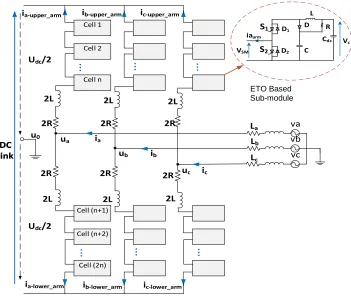
Figure 2-15. MMC structure with ETO thyristor based sub-modules
The clamp circuit reset time is defined in (2.35) and (2.36) shows the energy absorbed by the clamp, which is the charge delivered in this interval times voltage. The clamp circuit resistor is selected to keep the voltage across the clamp capacitor at a safe level for the switch in the worst case operating condition. The clamp capacitor is designed such that the maximum allowable ripple across it is 10% of the nominal value. Figure 2.15 shows the equivalent circuit of the ETO based sub-module with clamp circuit.
Cell 2 Cell n Cell (n+1) Cell (n+2) Cell 1 Cell (2n) DC link va vb vc DC link u0 ia-upper_arm ia-lower_arm
Udc/2
Udc/2
ia ib ic 2L 2L 2L 2L 2L 2L La Lb Lc ua ub uc
2R 2R 2R
2R 2R
2R
ib-upper_arm ic-upper_arm
Cdc L
R D
S1
S2 C
iaarm VSM
D1
D2
Vc
ib-lower_arm ic-lower_arm
Effect of clamp inductor on MMC circulating current
Circulating current is one of the critical issues of modular multilevel converter (MMC), which results in higher current stress and increases the converter losses [7, 8, 29]. MMC-HVDC system designed with ETO thyristors helps to decrease the circulating current by incorporating the internal snubber inductance of ETO to assist the converter’s arm inductor.
The clamp circuit diode conducts for a very short time so the equivalent circuit is similar to Figure 2-15 (b) for most of the cycle.
MMC is usually used for high voltage applications such as HVDC, which use several sub-modules in series to make the arm of the converter and build up the high voltage. Hence the clamp inductors add up to a significant value and can assist the converter’s arm inductor. In
the MMC shown in Figure 2-15, at least n sub-modules conduct in the phase leg at each instant to build the arm voltage so the equivalent inductance equals (2.37). The ETO thyristor based MMC-HVDC system is simulated in PSCAD with table 2-2 specifications and Figure 2-17 shows the circulating current comparison of the proposed system with IGBT based MMC-HVDC.
𝐿𝑒𝑞 = 𝑛𝑎𝑐𝑡𝑖𝑣𝑒× 𝐿𝑐𝑙𝑎𝑚𝑝 (2.39)
(a) (b)
Figure 2-16. ETO based Sub-module (a) when the clamp diode is on (b) when diode is off
Figure 2-17. Circulating current of conventional and proposed ETO based MMC-HVDC
Unbalance capacitor voltages mainly cause the circulating current through the leg of the converter. With the sub-module structure shown in Figure 2-16 every time the sub-module capacitor is inserted the clamp inductor is added to the arm for most of the cycle since the clamp circuit diode is only on for a very short time. A comparison of circulating current of conventional and proposed MMC with ETO sub-modules is shown in Figure 2-17. The new
C
dcS
1S
2ia
armV
SMD
1R
clampC
clampL
clampC
dcR
clampS
1S
2C
clampia
armD
1L
clamp0.1 0.11 0.12 0.13 0.14 0.15 0.16 0.17 0.18 0.19 0.2
MMC MODULATION TECHNIQUES
3.1 Introduction
Multilevel converters have been very attractive in both academia and industry in the past few decades and they have taken the place of two or three level converters in many applications. The main idea of multilevel converter is to introduce a topology that is capable of producing multilevel voltage from various DC sources. Multilevel converters have several advantages compared to two or three level converters in high power application. Multilevel converters are usually built by cascading some power modules that are identical in several topologies. Connecting the power modules increases the output voltage quality by generating more available voltage steps. Therefore the output of a multilevel converter usually has lower harmonics. The device voltage is also lower than the two or three level converters since each device has to withstand a portion of DC voltage. Since multilevel converters can generate more voltage levels they can be operated at much lower switching frequencies and the switching losses will be considerably smaller. Another reason for increased interest in these topologies is that they can implement controlled rotational movement in high power applications to equalize device stresses.
3.2 Modulation techniques
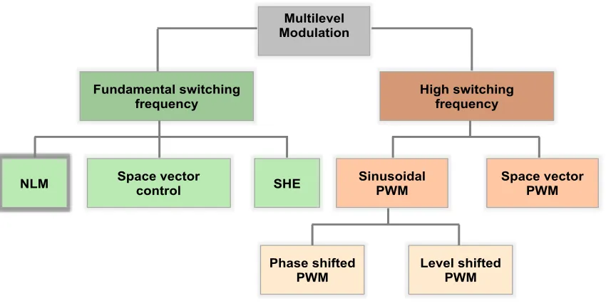
cost of increased switching losses. The fundamental frequency modulations techniques on the other hand have lower switching losses but decreased number of produced voltage levels. The criteria to select the proper modulation technique highly depend on the converter topology, design specification and application. Figure 3-1 shows a general classification of common multilevel modulation techniques. The high switching frequency modulation techniques are mainly a part of carrier based pulse width modulation. Space-Vector strategy, which has been used in three-level inverters and selective harmonic elimination are among the well-known low switching frequency modulation techniques used in multilevel converters. The following sections provide a brief overview of these modulation techniques [36].
3.3 Carrier based modulation techniques
The Pulse Width based Modulation (PWM) strategies used for a conventional inverter can be modified to use for multilevel inverters as well. Classic carrier-based sinusoidal PWM, which is a part of PWM family, is a very popular method in industrial applications for high switching frequency switching [37].
Figure 3-1. Classification of multilevel modulation methods
Sinusoidal PWM (SPWM)
Several modulation techniques are developed based on the classical sinusoidal PWM (SPWM) with triangular carriers to reduce the distortion in multilevel inverters. Three of the most common techniques are the following [38]:
The waveform of a carrier is phase shifted by 180o from the waveform of the next carrier (Alternate Phase Opposition Disposition, APOD).
All positive carrier waveforms are in phase, but the positive carriers have the opposite
Multilevel Modulation
Fundamental switching
frequency High switching frequency
Space vector PWM Sinusoidal
PWM
Level shifted PWM Phase shifted
PWM Space vector
control SHE
All the carrier waveforms are in phase (Phase Disposition, PD), as shown in Figure 3-2.
Figure 3-2. Phase disposition SPWM
3.3.1.1 Level shifted or phase disposition PWM
modules. The reference voltage can change between -MUdc and MUdc. The carriers of the first
module changes from zero to Udc, the second module changed between Udc and 2Udc and the
range increases to (M-1)Udc to MUdc for last modules to cover the whole voltage range. The
carriers are reordered for the negative side in the opposite order and there can be a phase shift between carriers. The switching pulses are derived by comparing the reference voltage waveform with the modules carrier. The state of each module is Udc when the reference is
higher than the positive carrier and same comparison is made for the negative carrier and the module outputs zero if none of these conditions are satisfied.
Udc if 𝑢𝑚𝑜𝑑∗ > 𝑢𝑐𝑎𝑟𝑝𝑜𝑠
𝑢𝑚𝑜𝑑 = -Udc if 𝑢𝑚𝑜𝑑∗ > 𝑢𝑐𝑎𝑟𝑛𝑒𝑔 0, otherwise
(3.1)
In this method the switching frequency of the converter output is fsw however the
modules have a varying switching frequency depending on the carrier position [39].
Figure 3-3. Phase shifted SPWM
3.3.1.2 Phase shifted PWM
The load-sharing problem of level shifted PWM is solved in phase shifted PWM technique. For multilevel inverters implemented using cascaded cells, the phase shifted SPWM technique is proven to be producing a load voltage with the smallest distortion. In this modulation technique, the carriers of N cascaded cells are phase-shifted by an angle of
θC=360o/ N. Figure 3-3 shows the basic principle of the Carrier-Shifted PWM modulation
technique. The carriers are usually allocated using two approaches. The first approach uses two carriers for each module with the amplitude of MUdc. The second method uses a 2MUdc
amplitude ranging from -MUdc to +MUdc and both methods use a carrier frequency of 1/ MTSW
Udc if −𝑢𝑚𝑜𝑑∗ < 𝑈𝑐𝑎𝑟 < 𝑢𝑚𝑜𝑑∗
𝑢𝑚𝑜𝑑 = -Udc if 𝑢𝑚𝑜𝑑∗ < 𝑈𝑐𝑎𝑟 < 𝑢 −𝑚𝑜𝑑∗
0, otherwise
(3.2)
3.4 Space vector modulation (SVM)
The two-level space vector pulse width modulation technique can be extended to more than three levels with appropriate modifications. The space vector d-q plane for a 6-level inverter is illustrated in Figure 3-5. Each point on the space vector plane represents a specific three-phase output voltage state of the inverter. The point (3, 2, 0), for example, means that with respect to ground, phase A is at 3VDC, phase B is at 2VDC, and phase C is at 0VDC. The
output voltages can be represented by an algebraic way, in terms of the switching states and DC-link capacitors is described in the following. For n = m-1, where m is the number of levels in the inverter, the following formula (3.3) applies [40].
𝑉𝑎𝑏𝑐0= 𝐻𝑎𝑏𝑐𝑉𝑐 (3.3)
𝑉𝑐 = [𝑉𝑐1 𝑉𝑐2 𝑉𝑐3…𝑉𝑐𝑛] , 𝑉𝑎𝑏𝑐0= [
𝑉𝑎0
𝑉𝑏0 𝑉𝑐0
] , 𝐻 = [
𝐻𝑎1
𝐻𝑏1 𝐻𝑐1
𝐻𝑎2
𝐻𝑏2 𝐻𝑐2
𝐻𝑎3
𝐻𝑏3 𝐻𝑐3
… 𝐻𝑎𝑛
𝐻𝑏𝑛 𝐻𝑐𝑛
] (3.4)
The elements of the above array are given by (3.3),
ℎ𝑎𝑗 = ∑ 𝛿(ℎ𝑛 𝑎− 𝑗)
𝑗 (3.5)
Where ha is the switching state, j is an integer from 0 to n, and δ(x) is defined as
𝛿(𝑥) = 1, 𝑖𝑓 𝑥 ≥ 0 (3.6)
Some particular output voltages can be generated by more than one switching combination. The corresponding states are then called redundant switching states. Redundant states are possible for lower modulation indices, or at any point other than those on the outermost hexagon shown in Figure 3-5. These states differ from each other by an identical integral value, for example, (3, 2, 0) differs from (4, 3, 1) by (1, 1, 1) and from (5, 4, 2) by (2, 2, 2).
In an m-level Diode-Clamped Inverter, the number of redundant states for an output voltage state (x, y, z) is given by m-1-max(x, y, z). The number of possible zero states is equal to the number of levels m. For a six-level diode-clamped inverter, the zero voltage states are (0, 0, 0), (1, 1, 1), (2, 2, 2), (3, 3, 3), (4, 4, 4), and (5, 5, 5). The number of possible switch
combinations is equal to the cube of the level m3. For the described 6-level inverter, there are 216 possible switching states. The number of distinct or unique states for an m-level inverter is given by (3.6).
𝑚3− (𝑚 − 1)3 = [6 ∑𝑚−1𝑛
𝑛−1 ] + 1 (3.8)
3.5 Selective Harmonic Elimination PWM
Selective harmonic elimination (SHE) is a method to generate PWM with low baseband distortion and was originally more successful in low switching frequency applications. Conventional PWM eliminates baseband harmonics for frequency ratios of 10:1 or greater but SHE has recently received attention because the digital implementation has become more common and there are also many solutions to SHE that was previously unknown. SHE is usually a two-step digital process. First is the offline calculation of the switching angels and second, storing angels in a look up table to be read in real-time [41].
𝑉(𝜔𝑡) =4𝑉𝐷𝐶
𝜋 ∑[cos(𝑛𝜃1) + cos(𝑛𝜃2) + ⋯ + cos(𝑛𝜃𝑠)]
𝑛
sin(𝑛𝜔𝑡)
𝑛 ,
𝑤ℎ𝑒𝑟𝑒 𝑛 = 1,3,5,7, … (3.9)
And θ1 to θs are to satisfy the condition that θ1< θ2<...<θs <π/2.
The amplitudes of all even harmonics are zero. The conducting angles, θ1, θ2, ..., θs
can be chosen such that the voltage total harmonic distortion is a minimum. Generally, these angles are chosen so that predominant lower frequency harmonics are eliminated. High frequency harmonic-components can be removed through the use of additional filter circuits [17, 42].
3.6 Nearest level modulation (NLM)
Nearest level modulation is one of the most suitable modulation techniques for MMC with large number of sub-modules. The conventional NLM technique works by dividing the reference voltage by individual sub-module voltage and generating the closest integer to the real number. Equations (3.10), (3.11), (3.12) and (3.13) show the total number of sub-modules in MMC arm, the AC reference voltage and number of calculated sub-modules by NLM upper and lower arm [43].
𝑈𝑆𝑀 = 𝑈𝑑𝑐
𝑁𝑗𝑢 = 𝑟𝑜𝑢𝑛𝑑(
0.5𝑈𝑑𝑐−𝑈𝑒𝑗𝑟𝑒𝑓
𝑈𝑐𝑟𝑒𝑓 ) (3.12)
𝑁𝑗𝑙 = 𝑟𝑜𝑢𝑛𝑑(0.5𝑈𝑑𝑐+𝑈𝑒𝑗𝑟𝑒𝑓
𝑈𝑐𝑟𝑒𝑓 ) (3.13)
For a grid connected MMC the reference of AC emf is obtained by active and reactive power demands [44]. The total number of sub-modules inserted in each phase is constant and defined by (3.14).
𝑁𝑗 = 𝑁𝑗𝑙+ 𝑁𝑗𝑙 (3.14)
Nj and Udc are constant to ensure that sub-module capacitor voltages stay around USM
however if no additional balancing technique is used the sub-module capacitor voltages might become unbalanced. Figure 3-6 shows the sub-module capacitor voltage with nearest level modulation when there is no capacitor voltage balancing in the control structure.
0 0.5 1 1.5 2 2.5
0.2 0.25 0.3 0.35 0.4 0.45 0.5 0.55
time (secs)
Submodul
e capacit
or vol
tages(
To overcome the problem of capacitor voltage fluctuation an additional part should be added to the modulation technique that measures the individual capacitor voltages and modifies the modulation to add the function of capacitor voltage balancing.
3.7 Proposed real time nearest level modulation (NLM) with
capacitor voltage balancing
To improve the performance of fundamental frequency based NLM, a real-time calculation of switching angels has been added to the method. The proposed algorithm inputs the reference modulation waveform from the system controller and calculates the switching angels such that the generated waveform by MMC is very close to the reference waveform. Figure 3-7 shows a zoomed in portion of the reference waveform and discrete steps generated by MMC sub-modules.
Vdc N 2Vdc
N 3Vdc
N
0
q1
Varm_k,ref(t)
Varm_NLM(t)
The proposed real-time modulation has two parts. First part is generation of the switching angels and second part is the capacitor voltage balancing. In order to achieve capacitor voltage balancing, individual capacitor voltages are measured at each controller time-step and sent to the controller. The measured voltages are sorted and at each switching instant (θi) and the switching decision is made with respect to the index of sorted capacitor voltage
matrix.
The sub-modules are in charging or discharging state according to the direction of current flowing through the sub-module. When the upper device is conducting the sub-module capacitor is inserted into the arm and as shown in Figure 2-2 when D1 is conducting the
sub-module capacitor will be in charging state. The sub-sub-module capacitor will discharge when S1
conducts. Thus to achieve balancing when the sub-modules are in charging state the ones with lowest capacitor voltages have to turn on first and in discharging condition the capacitors with highest voltage have higher priority. Figure 3-8 summarizes the proposed real-time modulation technique.
𝑛𝑎𝑐𝑡𝑖𝑣𝑒 = 𝑟𝑜𝑢𝑛𝑑(𝑉𝑎𝑟𝑚−𝑟𝑒𝑓
𝑉𝑆𝑀 ) (3.15)
Figure 3-8. Real-time NLM with capacitor voltage balancing Vdc1 Vdc2 . . . Vdcn Sorting Vdcmax . . . Vdcmin + (Index) θ1 θ2 . . . θn + Nactive (number of active SMs) NLM criteria Varm,ref 1Vdc 2Vdc . . . nVdc ( Discrete Voltage Steps) S1 S2 . . . Sn (Switching signals) Vdcmin . . . Vdcmax + (Index)
0 0.5 1 1.5 2 2.5