Survey paper on FIR Filter using
Programming Reversible Logic Gate
Yash Mishra, Prof. Vaibhav Jindal
M. Tech. Scholar, Department of Electronics and Communication, SISTech. Gandhinagar, Bhopal, India
Assistant Professor, Department of Electronics and Communication, SISTech. Gandhinagar, Bhopal, India
ABSTRACT: Reversible computing is a version of computing in which the computational system to a degree is reversible. An essential circumstance for reversibility of a computational version is that the relation of the mapping states of transition features to their successors have to always be one-to-one. Reversible logic has emerged as an change design technique to the conventional logic, ensuing in decrease energy consumption and lesser circuit area. In this paper, a review of an efficient architecture of the reversible FIR filter structure is presented. For reaching low electricity, reversible good judgment mode of operation is implemented inside the design. Vicinity overhead is the tradeoff inside the proposed layout. From the synthesis consequences, the proposed low electricity FIR filter architecture offers power saving when as compared to the conventional layout. The vicinity overhead is for the proposed structure.
KEYWORDS: FIR Filter, Reversible Gate, Peres Gate, Toffili Gate
I. INTRODUCTION
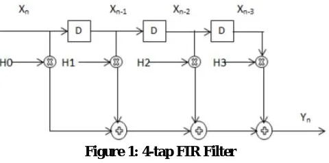
Virtual sign Processing is used in a huge variety of applications including radio, tv, video and many others. Its principal primary device Finite Impulse response (FIR) virtual filters. The filtering calls for arithmetic operations. The adder and multiplier module consume lots circuit region and energy. The complexity of the filter is specially because of the multiplication operation in FIR filter out. For low energy layout, enter bit width of the module is quite important. The adders, Wallace, dadda multipliers are implemented for filters to put off power intake because of unwanted records transitions [1]. In [2] they supplied a multiplier approach, based on add and shift technique and not unusual sub expression elimination for low vicinity, low electricity and high-speed implementation of FIR filters. Finite impulse reaction filters are extensively used in diverse DSP applications. The general FIR filter out can be expressed as the subsequent equation:
Where N represents the length of the FIR filter, the kth coefficient and x(n-ok) is the enter data at time on the spot n-th. where M is the tap range of the FIR filter, ck are the filter out coefficients, and x(n-k) is the enter signals. The above equations also can expressed in Z area as
Where H(z) is the transfer function of FIR filter in Z domain and is given by
dadda multipliers. The adders used for comparison are Ripple bring Adder, Carry look ahead adder, deliver save adder and carry select adder. all the combos of the adder and multipliers are used in the design. amongst all the aggregate the FIR filter out with deliver lookahead adder and Wallace multiplier gives higher end result while in comparison to the other combinations.
Figure 1: 4-tap FIR Filter
II. LITERATUREREVIEW
Kiran Joy et al. [1], guy has done wonders in his race from the stone age to the supersonic age. those wonders can be understood from the cutting-edge technologies. Technological improvements are getting a element and parcel of this world. an increasing number of technologies with lot of capabilities and advantages are springing up. Reversible logic is one such rising concept. One of the most important characteristics of reversible circuits is their less strength intake. as the generation improves, the variety of components and as a result the variety of transistors packed directly to the chip also will increase. This reasons boom in strength intake. Hence decreased strength consumption argued by the reversible logic concept has good enough significance inside the present state of affairs. Reversible common sense has a extensive software in low electricity VLSI circuits. This paper ambition at promoting the concept of reversible good judgment by way of imposing a model of a FIR clear out the use of the reversible Fredkin gate.
H. Thapliyal et al. [2], on this paper, we suggest the layout of two vectors testable sequential circuits primarily based on conservative common sense gates. The proposed sequential circuits based on conservative logic gates outperform the sequential circuits implemented in classical gates in phrases of testability. Any sequential circuit primarily based on conservative good judgment gates can be tested for classical unidirectional stuck-at faults the use of only two check vectors. the 2 test vectors are all 1's, and all zero's. The designs of two vectors testable latches, grasp-slave flip-flops and double area prompted (DET) flip-flops are provided. The significance of the proposed paintings lies inside the reality that it presents the design of reversible sequential circuits completely testable for any stuck-at fault by means of best two check vectors, thereby eliminating the want for any kind of scan-path access to internal reminiscence cells. The reversible design of the DET flip-flop is proposed for the first time within the literature. We also confirmed the application of the proposed technique in the direction of a hundred% fault insurance for single missing/extra cellular defect within the quantum-dot cellular automata (QCA) layout of the Fredkin gate. We are also providing a brand new conservative good judgment gate referred to as multiplexer conservative QCA gate (MX-cqca) that isn't reversible in nature but has similar homes because the Fredkin gate of working as 2:1 multiplexer. The proposed MX-cqca gate surpasses the Fredkin gate in terms of complexity (the variety of majority voters), velocity, and vicinity.
H. Thapliyal et al. [4], nanotechnologies, together with molecular QCA, are prone to excessive error costs. on this paper, we present the layout of testable reversible latches (D latch, T Latch, JK Latch, RS Latch), primarily based on reversible conservative common sense for molecular QCA. Conservative reversible circuits are a selected sort of reversible circuits wherein there could be an equal wide variety of Is inside the output as there could be on the input, similarly to 1- to-one mapping. The proposed latches require simplest two test vectors, all Os and all Is, for detecting any unidirectional caught-at faults. The layout of QCA layouts and the verification of the latch designs executed the use of the QCA designer tool are provided.
III. CONVERTIONAL FIR FILTER
FIR filter consists of multipliers, delay element and adders. The various multipliers and adders are described as follows:
Dadda multipliers are derived from parallel multipliers provided via Wallace in [5]. in the first degree of the
dadda multiplier, partial merchandise are fashioned by using the usage of N2 AND gates. Inside the 2d degree, the partial product matrix is reduced to a height of two. Dadda multipliers use a minimum number of (3,2) and (2,2) counters at every level all through the compression to gain the reduction. The discount process for Dadda compression bushes is given by way of the subsequent recursive set of rules [6].
1. Allow d1=2 and dj+1=[1.5.dj].dj is the height of the matrix for the jth level. Repeat until the largest jth level is reached wherein the original N height matrix incorporates as a minimum one column which has greater than djpartial products.
2. Within the jth level from the stop, region (three,2) and (2,2) counters as required to achieve a discounted matrix. best columns with extra thandj partial merchandise or with a view to have greater than dj partial merchandise as they get hold of includes less giant (three,2) and (2,2) counters are reduced.
3. Let j = j-1 and repeat step 2 till a matrix with a height of two is generated. This occurs while j= 1.
The eight x 8 Dadda multiplier calls for four discount ranges with matrix heights of 6,four, 3 and 2. 64 AND gates, 35 (three,2) counters, 7 (2,2) counters and 14 bit convey propagate adder are required to form sixteen-bit product.
The basic unit of ripple bring adder is full adder. it is able to be built by way of connecting complete adders in cascaded, with the carry out of the previous 1-bit full adder is given as convey-in to the next 1-bit full adder inside the chain. in this cascaded shape, perform propagates or ripples through the circuit. Ripple convey adder occupies smaller vicinity at the chip and offers high performance to random enter facts. The put off of the ripple convey adder depends at the length of the propagation direction. Because of this purpose, RCA isn't always suitable for circuits with non-random enter operands. Within the ripple deliver adder, the output is known most effective after the bring of the preceding level is produced. Therefore, the sum of the maximum large bit is only available after the deliver sign has rippled through the adder from the least extensive degree to the maximum widespread stage which is worst case addition. As the result, the very last sum and bring bits could be valid after a good sized postpone.
IV. REVERSIBLE GATE
Reversible common sense is gaining importance in regions of CMOS layout because of its low energy dissipation. The traditional gates like AND, OR, XOR are all irreversible gates. recall the case of conventional AND gate. It consists of inputs and one output. As a end result, one bit is misplaced every time a computation is completed. in line with the reality desk shown in Fig.1, there are three inputs (1, zero), (0, 1) and (zero, 0) that corresponds to an output zero. subsequently it isn't feasible to determine a unique enter that resulted in the output 0. with a view to make a gate reversible additional input and output strains are brought in order that a one to at least one mapping exists between the enter and output. This prevents the loss of statistics that is predominant purpose of strength dissipation in irreversible circuits. The enter that is introduced to an m x n characteristic to make it reversible is known as consistent enter (CI). all the outputs of a reversible circuit want not be used within the circuit. the ones outputs that aren't used within the circuit is called as garbage output (cross). The wide variety of garbage output for a specific reversible gate is not constant. the 2 fundamental constraints of reversible common sense circuit is
Fan out not allowed
o BASIC REVERSIBLE GATES
Numerous reversible gates have come out within the latest years. The maximum fundamental reversible gate is the Feynman gate and is shown in Fig.1. it is the most effective 2x2 reversible gate to be had and is typically used for fan out functions. do not forget the input B as consistent. when B is 0, the gate acts as a copying gate or a buffer where both the output lines comprise the enter A. while B is one, the complement of A is acquired on the output Q. The 3x3 reversible gates consist of Toffoli gate, Fredkin gate, New gate and Peres gate, all of which can be used to recognize various Boolean features. Fredkin gate is shown in Fig.2.The 4x4 reversible gates include TSG gate, MKG gate, HNG gate, PFAG gate etc.
Fig.3 shows the TSG gate. Some of the 4x4 gates are designed for implementing some important combinational functions in addition to the basic functions. Most of the above mentioned gates can be used in the design of reversible adders.
Several 4x4 and 5x5 gates have been described in the literature targeting low cost and delay which may be implemented in a programmable manner to produce a high number of logical calculations. The HNG gate, presented in [10], produces the following logical output calculations:
P
A
(1)
Q
B
(2)A
P
FG
A
B
Q
A
B
AC
B
A
Q
1
C
B
A
AB
C
A
R
1
FRG
A
P
B
A
Q
C
B
A
C
B
A
R
.
Peres Gate
A
P
Figure 2: Feynman gate
Figure 3: Fredkin gate
R
A
B
C
(3)
S
(
A
B
).
C
(
AB
D
)
(4)The quantum cost and delay of the HNG is 6. When D = 0, the logical calculations produced on the R and S outputs are the required sum and carry-out operations for a full adder. The quantum representation of the HNG is presented in Fig. 4.
A new programmable 4x4 reversible logic structure - Peres And-Or(PAOG) gate – is presented which produces outputs
P
A
(5)
Q
A
B
(6)
R
AB
C
(7)
S
(
AB
C
).
C
((
A
B
)
D
)
(8)Figure 6, shows the block diagram of the PAOG gate. This gate is an extension of the Peres gate for ALU realization.
V.METHODOFDESIGN
1. Design FIR filter using different types of reversible gate.
2. Design different types of programmable reversible gate and compared.
3. Design FIR Filter using different types of input and compared existing algorithm. 4. Hand calculation of delay and area in FIR Filter in different inputs.
5. All the modules design to different device family i.e. Spartan-3, Virtex-4 and Virtex-7.
A
P
B
A
Q
C
AB
R
)
(
)
)
((
C
AB
D
B
A
S
A
B
C
D
PAOG
A
B
C
D
V V V V+P
Q
R
S
Figure 5: Quantum Representation of the HNG Gate
VI.CONCLUSION
Hence the layout of low strength reversible FIR filter out structure is done. in the proposed technique the enter information samples and filter out coefficients are given as enter to the multipliers and adders designed the usage of reversible logic gates. The previous scheme is compared with the FIR filter out found out using regular multipliers and adders and the simulation effects, shows that the proposed FIR clear out designed using reversible Wallace multiplier and carry look ahead adder offers power saving ratio of about 18.1% with small area overhead of two.6%. The approach may be utilized in phonetic sign processing system.
REFERENCES
[1] Kiran Joy and Binu K Mathew, “Implementation of a FIR Filter Model using Reversible Fredkin Gate”, Control, Instrumentation, Communication and Computational Technologies (ICCICCT), 2014 International Conference on IEEEXplore: 22 December 2014.
[2] H. Thapliyal, N. Ran-Ganathan and S. Kotiyal, "Design of Testable Reversible Sequential Circuits", IEEE Transactions on VLSI, pp. 1-9, 2012.
[3] H. Thapliyal and N. Ranganathan, "Design of reversible latches optimized for quantum cost delay and garbage outputs", Proceedings of the
Twenty Third IEEE International Conference on VLSI Design, pp. 235-240, 2010.
[4] H. Thapliyal and N. Ranganathan, "Testable reversible latches for molecular qca", Proceedings of the Eighth IEEE Conference on
Nanotechnology, pp. 699-702, 2008.
[5] M. Chuang and C. Wang, "Reversible sequential element designs", Proceedings of the IEEE Asia and South Pacific Design Automation
Conference, pp. 420-425, 2007.
[6] S. Kumar Sastry Hari, S. Shroff, S. Noor Mahammad and V. Kamakoti, "Efficient building blocks for reversible sequential circuit design", Proceedings of the Forty Ninth IEEE International Midwest Symposium on Circuits and Systems, pp. 437-441, 2006.
[7] J.E. Rice, "A New Look at Reversible Memory Elements", Proceedings of the IEEE International Symposium on Circuits and Systems, pp. 243-246, 2006.