26
FFT Based Carrier Recovery with Lower
Processing Speed Using DSP Techniques
Vikas Kumar
1, Divya K. N
21,2
RFC-BEL Bangalore, MIT Manipal
ABSTRACT
Carrier recovery is one of most important block during demodulation. In closed loop system like Costas loop, stability of loop depends on the loop filter drastically, sometimes which become cumbersome when higher accuracy is required. In this paper, a novel approach to track carrier signal in terms of frequency and phase is explained. The concept of digital mixer and decimating filters are used to reduce processing speed. Fast Frequency Transform (FFT) working at lower operating frequency is used to track frequency to higher accuracy. The phase offset is tracked using digital phase comparator and digital phase shifter. The blocks are simulated in Matlab.
Key features: Frequency estimation, FFT, NCO, phase tracker
INTRODUCTION
Carrier recovery is an important block in communication receivers. Transmitters and receivers are working with independent synthesizers. Because of independency, the receivers are needed to be synchronized with transmitter in terms of frequency, phase and sampling instant. Synchronization for phase as well frequency is achieved by carrier recovery and synchronization for sampling instant is done by timing recovery. Signal received by receiver has frequency error as well as phase error. These error in received signal causes a rotation in signal space projections . If the rotation is large enough , the signal space projections for each possible symbol may lie in wrong decision region. As consequence , decision error occurs even with perfect timing synchronization. In receivers where carrier recovery is implemented in analog domain, local oscillator i.e. PLL is locked to the local oscillator used at transmitter in phase and frequency . In digital receivers, where carrier recovery is implemented after digitizing the intermediated frequency(IF), inbuilt NCO(Numerically controlled oscillator) is controlled to lock to carrier oscillator used at the transmitter. In this paper, carrier recovery is implemented digitally using DSP techniques.
CONCEPTUALDESIGNOFALGORITHM
In conventional carrier recovery based on FFT, the FFT core in FPGA is working at the same rate as of sampling frequency of analog to digital convertors(ADC) as shown in Eq. 1
Fcarrier=(Bin*Fs)/Point (1)
Where Fcarrier is carrier frequency calculated by FFT Bin is peak detection obtained by FFT
Fs is ADC sampling clock at which FFT core works Point is FFT-point used to calculate FFT
Eq. 1 relates the relationship between calculated carrier frequency and FFT core operating frequency. In conventional algorithm where core is working at high frequency cannot track carrier frequency with higher accuracy. In this paper, a different approach is implemented using FFT where higher accuracy is achieved using lower processing speed.
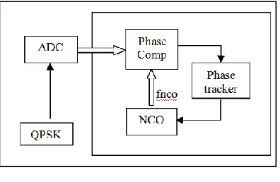
27 which is used to calculate frequency offset, decimation filter used to reduce processing speed, peak detector to detect the carrier frequency using FFT, phase increment adjuster block to adjust the frequency and an inbuilt NCO ipcore used to generate adjusted frequency fnco shown in Fig 1.
Fig. 1. Block Diagram to track frequency
Phase adjustment module consists of phase comparator block to find the offset in phase between received carrier irrespective of the phase change because of modulation, phase tracker to update the phase of inbuilt NCO, phase. The method is based on feed-forward technique but it is in the closed loop. If there is any offset in frequency or phase, loop is activated to adjust the change as shown in Fig 2.
Fig. 2 Block Diagram to track phase IMPLEMENTATION OF ALGORITHM
The algorithm is developed in MATLAB Simulink and then it is implemented on FPGA in VHDL language. QPSK modulated waveform generated from the vector signal generator with data-rate of 512kbps with carrier frequency of 6.3 MHz is used. The analog signal is digitized usinghigh speed ADC (Analog to digital convertor) at 100 MHz and it is interfaced to FPGA development kit. Inbuilt NCO of FPGA is programmed to generate a frequency of 6.25 MHz with an independent phase. As the carrier frequency of input modulated wave and inbuilt NCO are having a difference of 0.05MHz as well as independent phase, the NCO will be adjusted by the algorithm.
As the algorithm is based on the prior knowledge of carrier frequency. So the receiver has a prior knowledge of frequency which is used for modulation but it is unaware of the drifts during the physical parameters. In this paper, the carrier frequency is set to 6.25 MHz but because of physical drift, it is assumed that received signal has a carrier frequency of 6.3 MHz. To track the frequency to high resolution , mixer approach is used .
28 The multiplier gives an output of 0.05 MHz and 12.55 MHz which is updated at 100 MHz. The frequency of interest here is 0.05 MHz. To filter out 12.55 MHz from the output spectrum as well to lower the processing speed , it is decimated by 10 times. To estimate the frequency, FFT block is used as shown in Fig. 1.
From Eq. 1 it is clear that the as the processing speed of FFT core is reduced , the minimum detectable frequency by FFT core is improved. To utilize this concept, mixer output is decimated. In implementation side, Fs is kept 10 MHz after using decimating filter which decimated data by 10 times ie from 100 MHz to 10 MHz. Using Eq.1 for 256 point FFT at 10 MHz sampling clock, gives a resolution of 39.0625 KHz minimum frequency offset which can be detected whereas the conventional FFT based carrier gives a resolution of 390.625 KHz. The new approach solves the problem of higher resolution at lower processing speed .
The next block in frequency tracking is Phi cal ie phase increment calculator block which acts as interfacing block between the Phi Mod ie phase increment modulator block as shown in Fig.1. The relationship between the frequency estimated by FFT core and phase increment required to adjust NCO frequency i.e. fnco is given by Eq. 2
FTW=(Bin*NCO full scale)/Point (2)
Where FTW is Frequency tuning word which decides the frequency generated by NCO which is 32 bit.
In this approach, because of mixer approach, there is an ambiguity that the frequency offset obtained is greater than on lesser than the initial NCO frequency. To solve the ambiguity, a different approach is followed. Instead of directly mixing the incoming signal, the signal is stored in FPGA in RAM. In stage I, the stored signal from RAM is fetched at the sampling speed and it mixed to give the offset frequency. In stage II, the offset is added to the inbuilt NCO and error is calculated. In stage III, the offset is subtracted from the inbuilt NCO and corresponding error is calculated. The error from stage II and stage III are compared. The lesser error shows the validity of offset which is used for real time. After this the NCO ie fnco as shown in Fig. 1 is locked with input modulated wave with respect to frequency.
Once the inbuilt NCO is locked to input carrier frequency, now it has to lock to input carrier phase irrespective of the phase modulation occurred because of data. The algorithm is shown in Fig. 2. The main block are phase comparator, phase tracker and NCO. The frequency adjusted NCO is used as one of the input to digital phase comparator whereas the other input is digitized QPSK signal. The phase comparator is designed such that irrespective of the phase modulation because of the data, the reference phase difference between the NCO and QPSK is estimated. In digital domain, resolution of phase detector depends on the number of bits used to implement phase comparator. In the algorithm, 14 bit phase comparator is used. The resolution is given in Eq. 3
Resol =360/8192 (3)
Where 8192 represents the number of full scale14 bits used for implementation and Phase_resol gives the resolution achieved.
The phase difference calculated from the digital phase comparator is normalized so that the module can work for wide dynamic range of input. The normalized input is fed to phase tracker block to make required adjustment in phase of nco. The inbuilt NCO ie fnco is now in synchronization to input QPSK modulated wave with respect to phase as well as frequency. The output is fed to further demodulating blocks.
RESULTS
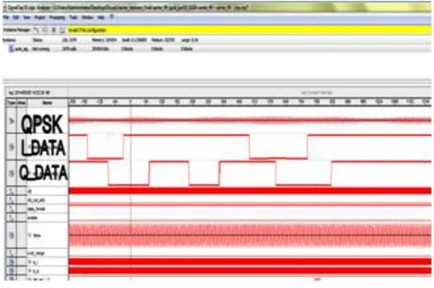
29 Fig. 3 Digitized QPSK
Fig. 3 shows the digitized QPSK data written as QPSK. Inbuilt NCO is locked to the frequency of digitized QPSK which is shown by fnco. Fig 5 shows the demodulated data.
Fig. 4 Demodulated Data REFERENCES
[1]. Digital Communications - A Discrete Time Approach - Michael Rice
[2]. Timing And Carrier Recovery Techniques In DSP Based Digital - Shruti Sheth and Fred Harris.
[3]. A New Frequency Pre-estimation Aided Carrier Recovery Algorithm For Multimodal Signal Systmem-Wang [4]. Carrier Receovery Using FFT- Xu Yang, XiaoWei Cui, MingQuau Lu and ZhenMing Feng
[5]. Design And Implementation Of A Multi-Carrier Demodulator -H.Ho,V.SZWARC,C-LOO and T-Kwasniewski [6]. Frequency Offset And Symbol Timing Recovery In Flat-Fading channels: A cyclostationary approach-Fulvio Gini
,Georgios B Giannakis.
[7]. Real Time DSP based Carrier Recovery With Unknown Doppler Shift-Philip L De Leon
30 BIODATAOFAUTHORS
Vikas Kumar-Obtained his B.E from UVCE Bangalore in 2012.He joined BEL in 2012 and since then he is working in RF group as Deputy Engineer. He has worked on L-Band TR modules used in Radios, FPGA based control cards for radio relays, Signal processing for proximity sensor used in Collision Avoidance, Ultra low phase noise synthesizers in L Band, Signal processing for Digital Receiver and Exciters.