DOI : 10.32628/CSEIT1952390
Performance Analysis of Fully Differential Double Tail Dynamic Comparator
Priyesh P. Gandhi, Ph. D
Principal, Sigma Institute of Engineering, Vadodara, Gujarat, India
ABSTRACT
This paper presents a novel fully differential double tail dynamic comparator that exhibits lower offset voltage than the conventional dynamic comparators. This paper comprises a novel fully differential double tail high performance comparator suitable for low-voltage low-power applications. A fully differential double tail comparator has been designed to meet the necessity of low offset voltage for optimum power with high speed. The expression for the calculation of the offset voltage of the proposed comparator is derived. These expressions corroborate previously stated results with analytical support as well as providing useful insight for the design of fully differential double tail dynamic comparator by analyzing the influence of each transistor pair individually. Transistor mismatch analysis is carried out for offset voltage to fully explore the trade-offs in the design of comparator. In proposed comparator offset voltage is significantly reduced for optimum power. Authors have proposed novel architecture of dynamic voltage comparator which is differential and double tail and verified the architecture by simulation in 180nm CMOS technology with ±0.9V supply. The Post-layout simulation results illustrates that a comparator designed with the proposed techniques is 45% faster, and 30% more power efficient and exhibits 91% low offset as compared with conventional comparator, which is the fastest among the conventional comparators.
Keywords : Comparator, Differential Dynamic Comparator (DDC), Fully Differential Double Tail Dynamic Comparator (FDDTDC), Analog to Digital Converters (ADCs), Propagation delay, Offset Voltage, Power Dissipation.
I. INTRODUCTION
The incredible demand for high performance ADC is pushing towards the use of dynamic comparator to maximize speed and to optimize the power. In most of all ICs, a significant component called ADC, that bridges the gap between the analog world and the digital systems, is used. The comparator forms the main heart of any ADC architecture used in contemporary technology for conversion from analog to digital and vice-versa. The accuracy of such converters has strong relation on design of inter stage gain amplifier and comparator.
The performance of a comparator will determine overall performance of A /D Converter because of large number of comparators is used compared to inter stage gain amplifier. The large number of comparator makes it the most critical block of a ADC architecture, not allowing efficient background calibration of all the comparators which directly affects the effective resolution of the ADC due to the comparator input offset voltage.
prime concern for high speed digital system and speed of comparator is the key factor. [3]. The prerequisite to extend the battery life of the digital system, speed and accuracy of the ADC is major concern; for comparator low offset, high speed with low power consumption is desirable. In recent years the emphasis has been given towards the design of high speed comparator with power optimization. The accuracy of the comparators confines due to offset voltage because of mismatch in Vth, β, parasitic and output load capacitance [8-10]. The comparator circuits should be immune to speed, power and offset trade off.
Several approaches have been proposed in the literature discussed either differential architecture or double tail architecture with offset voltage varies from 10mV to 50mV. In comparators, a lower offset comes at the cost of bigger transistor dimension therefore it will lead to more power dissipation and increased in delay. In addition, the traditional comparators are difficult to design and there are not many design procedures to lower the offset voltage. To decrease the power utilization and the area of comparators, dynamic comparators are proposed [3-6]. However, such comparators generally experience comparatively large offset voltage in comparison to static comparators [6,7]. Some designs have been proposed for dynamic comparators in the literatures. The dynamic comparators are categorized in to three groups: Resistor divider [6], Differential pair and Charge Sharing dynamic comparator [6]. Other structures are mainly derived from these architectures [3–8].
The designs proposed in literature, some are concerned with speed [7], few give emphasis to power optimization and high resolution [2], some on offset cancellation [6]. In this paper authors come out with novel design one with low offset with optimum power dissipation.
In order to break the deadlock between offset and power consumption authors have proposed novel architecture which combines the features of differential pair and double tail. The proposed architecture is more robust against any misalignment and non idealities. More importantly, it involves a significantly smaller input offset voltage without a significant rise in power and delay.
With two additional transistors inserted between output and input of the conventional dynamic comparator and converting into fully differential double tail dynamic comparator, which shows low propagation delay, with low offset voltage without any offset calibration techniques which requires more number of devices and calibration time more power hungry design strategies with optimum power and higher clock rate with the similar area, was implemented.
The paper is organized in 5 sections; Section 2 discussed the existing architecture of Differential Dynamic Comparator (DDC). Section 3 presents the novel architecture of Fully Differential Double Tail Dynamic Comparator (FDDTDC). Section 4 discussed the simulation results, section 5 concludes the paper.
1.1 Existing Architectures of Differential
Dynamic Comparator
The existing Differential Dynamic Comparator (DDC) architecture is illustrated in Fig. 1[7]. When
Figure 1. Differential Dynamic Comparator (DDC).[7]
All the input transistors are of the equal dimension and no imbalance is present and to ensure all input transistors M1 to M4 have same currents the differential pair Vin+ and Vref+ (and Vin- and Vref-) are combined in single differential pair[4,5]. During the time of decision all input transistors will contribute respectively.
The internal nodes are reset to VDD when comparator is in ideal mode and help comparator to retune all the nodes prior to the comparator enters into the evaluation mode.
II. Proposed Comparator
The Fully Differential Double Tail Dynamic Comparator (FDDTDC) is shown in Fig. 2. Some modification has been made to the structure in comparison to the structure shown in Fig. 1. Transistors M13 and M14 are removed from the structure because transistors MA and MB will serve the same purpose to reset the internal nodes D1 and D2. On the removal of two clock driven transistors M13 and M14 the power dissipation of the comparator has drastically reduced in comparison to DDC. The
FDDTDC can work at lower supply voltages as compared to DDC due to less stacking.
Figure 2. Fully Differential Double Tail Dynamic Comparator (FDDTDC).
2.1 Operation of the Proposed Comparator
Reset Mode: When ΦClk is low, transistors MA, MB, M9 and M12 are on. Out+ and Out- are precharge to VDD similarly internal nodes D1 and D2 are retune to VDD.
Comparison Mode: When ΦClkis high ΦClk,B is active, transistors MA, MB, M9 and M12 are off. Out+ and Out -are discharge to ground through M1 - M4.
The voltage at Vin+ is higher than the voltage at Vin-, Out- is discharged faster than Out+. Addition of two transistors of the MA and MB convert the single tail comparator into double tail comparator with differential input and on removal of transistors M13 and M14 reduced the power dissipation and reduces the offset voltage and propagation delay.
2.2 Performance Analysis and Design Trade-Offs
and. In practice, comparator design is a multi-dimensional optimization problem because most of these constraints deal with each other. This trade-off presents many challenges in the design of high performance comparator to arrive at an optimum or compromise solution requires intuition and experience [18].
2.2.1 Offset Analysis
By definition, the offset voltage VOS of the comparator equals to the differential input voltage that establishes the condition Vout+ = Vout-.
In the beginning of the decision moment, M1 to M4 and M5 are in the saturation region. This is the main reason of the low sensitivity of this topology to the transistor mismatch as will be demonstrate hereafter. If all the transistors of the two differential pairs have
the same dimensions, β1=β2=β3=β4, then in the balanced point the two output currents are equal [8-9].
The threshold voltage Vth andµCox can be explicit in terms of a nominal part and a deviation part owing to mismatch between M7 and M8. For ease of calculation collective deviation between µ and Cox can be consider as only deviation in mobility µ. [8-9].
µ7 = µn+ ∆µ7 (8)
µ8 = µn+ ∆µ8 (9)
Vt7 = Vtn+ ∆Vt7 (10)
Vt8= Vtn+ ∆Vt8 (11)
The random mismatch in the threshold and mobility of transistor pair can be modeled as follows [8-9]:
transistor pair in layout. In 180nm CMOS process, for proposed Fully Differential Double Tail Dynamic Comparator is as follows:
For Differential Dynamic Comparator static random
offset voltage σVos is as follows:
𝜎𝑉2𝑂𝑆= (𝜎𝑉2𝑂𝑆_𝑀5𝑀6+ 𝜎𝑉2𝑂𝑆_𝑀1𝑀4+ 𝜎𝑉2𝑂𝑆_𝑀2𝑀3
+ 𝜎𝑉2𝑂𝑆_𝑀7𝑀8+ 𝜎
𝑉𝑂𝑆_𝑀10𝑀11
2 )1⁄2 (19)
2.2.2 Delay Analysis
The delay is characterized as the time between the start of the amplification phase and the time where 50% of the latch final output is reached. Based on this definition, the inner latch delay can be calculated from derivations presented in [16-17].
The delay of the comparator consists of two key parts, t0 and tlatch [13].
Delay of Differential Dynamic Comparator (DDC) as follow:
𝑡𝑑𝑒𝑙𝑎𝑦= 2
Delay of FDDTDC as follow:
𝑡𝑑𝑒𝑙𝑎𝑦= 𝑡0+ 𝑡𝑙𝑎𝑡𝑐ℎ= 2
2.2.3 Power Analysis
In dynamic comparator power is expressed as below influence the most on the power consumption of the comparator.
III. Simulation Result
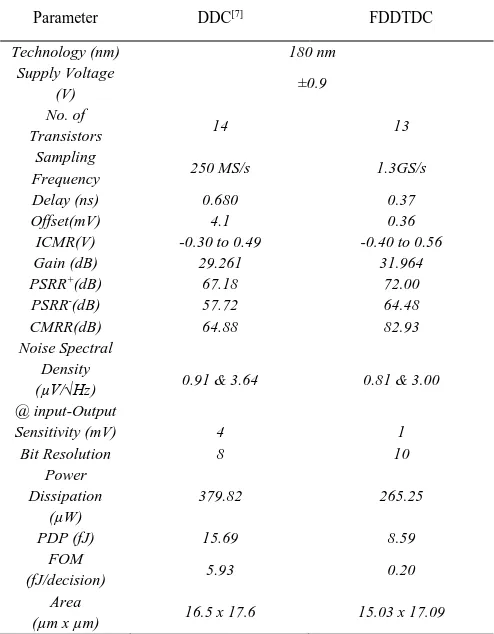
To verify its operation and the consistency with the analytical derivations including delay, offset ICMR, frequency response and input –output noise spectral density. The circuit operates from a ± 0.9V power supply. The simulation results shown in Fig. -4 to 18, the delay of FDDTDC comparator is 0.37ns, offset voltage is 0.36mV, ICMR is -0.40 V to 0.56V with power consumption of 216.37mW which is quite low in comparison Differential Dynamic Comparator. The FDDTDC can successfully resolve difference of 1mV (10 bit resolution for 1Vp-p input swing) at 1.3GS/S. Considering that there is no extra circuitry require for offset cancellation, the new-flanged design is appropriate for applications demanding high resolution, high speed with optimum power.
2.3Simulation Results of DDC
Figure 5. Offset Voltage of DDC. 2.4 Simulation Results of FDDTDC
Figure 10. Transient Analysis of FDDTDC.
Figure 11. Offset Voltage of FDDTDC.
Figure 12. ICMR of FDDTDC.
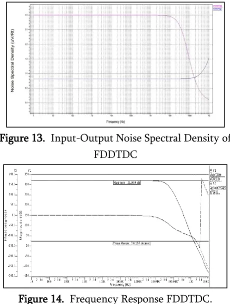
Figure 13. Input-Output Noise Spectral Density of FDDTDC
Figure 14. Frequency Response FDDTDC.
Fig.-9 and 15 shows comparator layouts. Particular care was taken in the layout to avoid mismatch to avoid affecting delay and power of the comparator.
Figure 17. Delay v/s Supply Voltage.
Fig.-16 illustrates the sensitivity of the input referred offset to input common mode voltage (VCM). The Proposed Fully Differential Double Tail Dynamic Comparator has low offset voltage as compared to DDC mentioned in the Fig. 1.
Fig.-17 demonstrates the simulation results of the delay of FDDTDC versus variation in supply voltage. The delay of the FDDTDC is significantly reduced with higher differential input voltage.
Figure 18. Mismatch Analysis.
Figure 18 illustrates the mismatch analysis between transistor pairs and effects of offset voltage due to individual pairs as mentioned in equation (18) and (19).
Table 1 evaluates the performance of the FDDTDC with the DDC. The overall noise spectral density at the input is similar in the case of DDC and DDTDC. The FDDTDC comparator provides the high gain,
low offset, with high dynamic range with better sensitivity at low input with power optimization with considerable reduction in delay.
As Table 2 shows, the FDDTDC has the very low offset and lowest FOM energy dissipated per conversation for optimum power.
Table 1: Performance Comparison
Parameter DDC[7] FDDTDC
Technology (nm) 180 nm
Supply Voltage
(V) ±0.9
No. of
Transistors 14 13
Sampling
Frequency 250 MS/s 1.3GS/s
Delay (ns) 0.680 0.37
Offset(mV) 4.1 0.36
ICMR(V) -0.30 to 0.49 -0.40 to 0.56
Gain (dB) 29.261 31.964
PSRR+(dB) 67.18 72.00
PSRR-(dB) 57.72 64.48
CMRR(dB) 64.88 82.93
Noise Spectral Density (µV/√Hz) @ input-Output
0.91 & 3.64 0.81 & 3.00
Sensitivity (mV) 4 1
Bit Resolution 8 10
Power Dissipation
(µW)
379.82 265.25
PDP (fJ) 15.69 8.59
FOM
(fJ/decision) 5.93 0.20
Area
(µm x µm) 16.5 x 17.6 15.03 x 17.09
Table 2: Performance Summary and
Comparison
Reference [10-12] [13] [14] This
Work
Technology (nm) 90 180 90 180
Supply Voltage
(V) 1 1.2 1.0 ±0.9
Sampling
Frequency(GS/s) 3.0 0.5 1 1.3
Delay (ns) 0.17 0.29 0.15 0.37
Resolution (bits) -- -- -- 10
Offset(mV) 16.3 7.8 33 0.36
Power(µW) 162 329 51 265.25
PDP (fJ) -- -- -- 8.59
IV. CONCLUSION
A novel design structure of Fully Differential Double Tail Dynamic Comparator for high performance ADC is proposed with comprehensive offset analysis and expressions is derived. The simulation results illustrates that a comparator designed with the proposed techniques is 45% faster, and 30% more power efficient. The FDDTDC exhibits 91% low offset without any power hungry offset cancellation circuits as compared with conventional comparator. The FDDTDC makes a superior trade-offs among speed, resolution, power, offset and area.
V. REFERENCES
[1]. R. Jecob Baker, Harry W. Li, David E. Boyce,
“CMOS Circuit Design, Layout and Simulation”, IEEE Press Series on
Microelectronic Systems, pp.685-699, 1997. [2]. Phillip E. Allen, Douglas R. Holberg, “CMOS
Analog Circuit Design”, Oxford University
Press, Second Edition, pp.439-488, 2002.
[3]. L. Sumanen; M. Waltari; K. Halonen, “A
mismatch insensitive CMOS dynamic comparator for pipeline A/D converters”,. 7th
IEEE International Conference on Electronics, Circuits and Systems ICECS 2000, vol.1, pp. 32
– 35, Dec. 2000.
[4]. L. Sumanen, M. Waltari, V. Hakkarainen, K. Halonen, "CMOS Dynamic Comparators for Pipeline A/D Converters," IEEE ISCAS, vol. 5, pp. 157-160, May 2002.
[5]. T. W. Matthews, P. L. Heedley, "A Simulation Method for Accurately Determining DC and Dynamic Offset in Comparators," IEEE MWSCAS, pp. 1815-1818, Aug. 2005.
[6]. P. Uthaichana, E. Leelarasmee, “Low Power
CMOS Dynamic Latch Comparators”, TENCON
2003, Conference on Convergent Technologies
for the Asia-Pacific Region, pp605-608 Vol.2 Oct 2003.
[7]. Vipul Katyal, Randall L. Geiger and Degang J.
Chen, “A New High Precision Low Offset
Dynamic Comparator for High Resolution High Speed ADCs”, IEEE Asia Pacific Conference on
Circuits and Systems, 2006 (APCCAS 2006) pp.5-8, Dec.2006.
[8]. Jun He, Sanyi Zhan, Degang Chen, Randall L.
Geiger, “A Simple and Accurate Method to
Predict Offset Voltage in Dynamic
Comparators”, IEEE International Symposium on Circuits and Systems, 2008, pp. 1934-1937, May. 2008.
[9]. Jun He, Sanyi Zhan, Degang Chen, Randall L. Geiger, "Analyses of Static and Dynamic Random Offset Voltages in Dynamic Comparators", IEEE Transactions on Circuits and Systems I: Regular Papers, ISSN 1549-8328 ISSN 1549-8328, vol. 56, pp. 911-919, May. 2009,.
[10]. Heung Jun Jeon, Yong-Bin Kim, “A Low-offset High-speed Double-tail Dual-rail Dynamic
Latched Comparator”, GLSVLSI '10
Proceedings of the 20th symposium on Great lakes symposium on VLSI, pp. 45-48, Sep. 2010. [11]. Heung Jun Jeon and Yong-Bin Kim, “A Novel
Low Power, Low Offset, and High Speed CMOS
Dynamic Latched Comparator”, Analog
Intergrated Circuit Signal Processing, July. 2011.
[12]. Heung Jun Jeon, Yong-Bin Kim, “A CMOS Low
Power Low Offset and High-Speed Fully
Dynamic Latched Comparator” , IEEE SOC
International Conference (SOCC), pp. 285-288, Sep. 2010.
[13]. S. Babayan-Mashhadi, R. Lotfi, “Analysis and
Design of a Low-Voltage Low-Power
Double-Tail Comparator” IEEE Transactions on Very
[14]. M. Hassanpourghadi, M. Zamani and M.
Sharifkhani, “A Low-Power Low-Offset Dynamic Comparator for Analog to Digital
Converters”, Microelectronis Journal, Elsevier,
pp.256-262. Feb 2014.
[15]. Dhanisha N. Kapadia, Priyesh P. Gandhi
“Design and Comparative Analysis of
Differential Current Sensing Comparator in Deep Sub -Micron Region”. Proceedings of2013
IEEE Conference on Information and Communication Technologies, pp. 21-25, April. 2013..
[16]. Dhanisha N. Kapadia, Priyesh P. Gandhi,
“Implemnation of CMOS Charge Sharing
Dynamic Latch Comparator in 130nm and
90nm Technologies”. Proceedings of 2013 IEEE
Conference on Information asnd Communication, pp. 16-20, April. 2013.
[17]. IIi Shairah Abdul Halim, Nurul Aisyah Nadiah
Binti Zainal Abidin, A’zraa Afhzan Ab Rahim, “Low Power CMOS Charge Sharing Dynamic Latch Comparator using 0.18µm Technology”,
IEEE Regional Symposium on Micro and Nanoelectronics (RSM), pp.156-160,Sep.2011. [18]. M. J. Taghizadeh Marvast, M. A. Mohd Ali,
“High Speed Comparator for Flash ADC and
UWB Application in 130nm CMOS
Technology”, IEEE Conference on Signal and
Image Processing Applications, pp. 402-405, 2009.
[19]. Nurul Iffah Mohamad Azizi, Siti Hawa Ruslan,
“Design of A Low Power 0.25µm CMOS Compartor for Sigma-Delta Analog -to- Digital
Converter”, IEEE Student Conference on
Research and Development (SCOReD), pp.638-642, Dec. 2015.
[20]. Dinanath N. Donadkar, Sheetal U. Bhandari,
“Review on Comparator Design for High Speed ADCs” IEEE International Conference on Computing Communication Control and Automation, pp. 974-978, Feb. 2015.
[21]. Samaneh Babayan-Mashhadi, Mojtaba Daliri,
Reza Lotfi, “Analysis of Power in Dynamic Comparators”, 21st Iranian Conference on
Electrical Engineering (ICEE), 2013 pp.1-4, May.2013.
About Author
Dr. Priyesh P. Gandhi was born in Diu, Inida in 1983. He received the B. E E & C from the HNGU, Patan, India in 2004 and M.Tech in VLSI Design in 2010 and Ph.D in Electronics & Communication Department with specialization in VLSI Design in 2018 from the Nirma University, Ahmedabad. Presently working as a Pincaipal at Sigma Institute of Engineering, Vadodara from March 2019. His Current research interest includes low power low voltage analog and mixed signal integrated circuit.
Cite this article as :
Priyesh P. Gandhi, "Performance Analysis of Fully Differential Double Tail Dynamic Comparator ", International Journal of Scientific Research in Computer Science, Engineering and Information Technology (IJSRCSEIT), ISSN : 2456-3307, Volume 5, Issue 2, pp.1301-1310, March-April-2019.

![Figure 3. Design Trade-OffsOffset Analysis [18]](https://thumb-us.123doks.com/thumbv2/123dok_us/1048940.1131139/4.595.305.552.71.298/figure-design-trade-offsoffset-analysis.webp)