Modeling and Analysis of Printed Antenna
Using Finite Difference Time Domain
Algorithm
Dr.T.SHANMUGANANTHAM *, Dr.S.RAGHAVAN**
*Assistant Professor, Department of Electronics Engineering School of Engineering & Technology, Pondicherry University
Pondicherry– 605 014, India
Abstract:- An efficient Finite Difference Time Domain algorithm is developed for printed patch antenna without
using commercial software packages like IE3D, HFSS, ADS, and CST. Printed patch antennas which are small and conformity are demanded from the points of carrying and designing. Numerical results of return loss, current distribution, electric field and magnetic field components are plotted. The results presented for the fundamental parameters of the Microstrip patch antenna useful for wireless communications and RFID applications.
Key Words:- Finite Difference Time Domain (FDTD), Printed Antenna, Numerical Technique, Return loss, Current distribution.
I. INTRODUCTION
Finite-difference time-domain (FDTD) is a popular computational electrodynamics modeling technique. Since it is a time-domain method, solutions can cover a wide frequency range with a single simulation run. The FDTD method belongs in the general class of grid-based differential domain numerical modeling methods. The time-dependent Maxwell's equations (in partial differential form) are discretized using central-difference approximations to the space and time partial derivatives. The resulting finite-difference equations are solved in either software or hardware in a leapfrog manner: the electric field vector components in a volume of space are solved at a given instant in time; then the magnetic field vector components in the same spatial volume are solved at the next instant in time; and the process is repeated over and over again until the desired transient or steady-state electromagnetic field behavior is fully evolved. The basic FDTD space grid and time-stepping algorithm trace back to a seminal 1966 paper by Kane Yee [1]. The descriptor "Finite-difference time-domain" and its corresponding "FDTD" acronym were originated by Allen Taflove [2]. Since about 1990, FDTD techniques have emerged as primary means to computationally model many scientific and engineering problems dealing with electromagnetic wave interactions with material structures. As summarized in Taflove & Hagness (2005), current FDTD modeling applications range from near-DC (ultralow-frequency geophysics involving the entire Earth-ionosphere waveguide) through microwaves (radar signature technology, antennas, wireless communications devices, digital interconnects, biomedical imaging/treatment) to visible light. In 2006, an estimated 2,000 FDTD-related publications appeared in the science and engineering literature. Every modeling technique has strengths and weaknesses, and the FDTD method is no different. FDTD is a versatile modeling technique used to solve Maxwell's equations. It is intuitive, so users can easily understand how to use it and know what to expect from a given model. FDTD is a time-domain technique, and when a broadband pulse is used as the source, then the response of the system over a wide range of frequencies can be obtained with a single simulation. This is useful in applications where resonant frequencies are not exactly known, or anytime that a broadband result is desired. FDTD calculates the E and H fields everywhere in the computational domain as they evolve in time, it lends itself to providing animated displays of the electromagnetic field movement through the model. This type of display is useful in understanding what is going on in the model, and to help ensure that the model is working correctly. It also requires that the feed location be far enough from any geometrical features sothat no reflections return to the feed location before the source is removed and the outer absorbing boundary is switched on.
the effects of apertures to be determined directly. Shielding effects can be found, and the fields both inside and outside a structure can be found directly or indirectly. FDTD uses the E and H fields directly. Since most of the antenna applications are interested in the E and H fields, it is convenient that no conversions must be made after the simulation has run to get these values.
The time dependent Maxwell’s curl equations in free space are
H
t
E
0
1
(1)E
t
E
0
1
(2)E and H are vectors in three dimensions. For one dimensions condition Ex and Hy becomes,
z
H
t
E
x y
0
1
(3)z
E
t
H
y x
0
1
(4)These equations are plane wave with the electric field oriented in the x direction, the magnetic field oriented in the y direction and travelling wave in the z direction. Difference approximations for both the temporal and spatial derivatives gives,
x k H k
H t
k E k
E yn
n y n
x n
x
2 1 2
1 1
0 2
1 2
1
(5)
x k E k E t
k H k
H n
x n
x n
y n
y
12
2 1
0 1
1 1
2 1 2
1
(6)
II. DETERMINING THE CELL SIZE
Choosing the cell size to be used in an FDTD formulation is similar to any approximation procedure, enough sampling points must be taken to ensure that an adequate representation is made. The number of points per wavelength is dependent on many factors. However, a good rule of thumb is 10 points per wavelength. Suppose we are running simulation at 20 GHz. In free space, EM energy will propagate at the wavelength,
m
m
GHz
c
015
.
0
10
20
sec
10
3
20
98 0
0
(7)If we were only simulating free space
cm
x
010
0
.
15
(8)However, if we are simulating EM propagation in Microstrip Patch antenna, for instance, we must look at the wavelengths with the dielectric constant. For Microstrip patch antenna has relative dielectric constant is 2.2 at 20 GHz, so
cm
GHz
c
m
0
.
1
20
2
.
2
0
(9)And we would probably select a cell size of one centimeter.
III. FREE SPACE FORMULATION
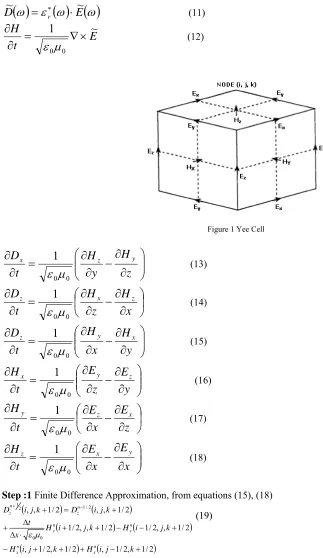
E and H fields are assumed interleaved around a cell whose origin is at the location i, j, k. Every E field is located ½ cell width from the origin in the direction of its orientation, every H field is offset ½ cell in each direction except that of its orientation.
We will start with Maxwell’s equations,
H
t
D
~
1
~
E
D
r~
~
(11)E
t
H
1
~
0 0
(12)Figure 1 Yee Cell
z
H
y
H
t
D
x z y0 0
1
(13)
x
H
z
H
t
D
z x z0 0
1
(14)
y
H
x
H
t
D
z y x0 0
1
(15)
y
E
z
E
t
H
x y z0 0
1
(16)
z
E
x
E
t
H
x z y 0 01
(17)
x
E
x
E
t
H
z x y0 0
1
(18)Step :1 Finite Difference Approximation, from equations (15), (18)
, 1/2, 1/2 , 1/2, 1/2
2 / 1 , , 2 / 1 2 / 1 , , 2 / 1 2 / 1 , , 2 / 1 , , 0 0 2 / 1 2 1 k j i H k j i H k j i H k j i H x t k j i D k j i D n x n x n y n y n z n z (19)
IV. ABSORBING BOUNDARY CONDITIONS
One of the most flexible and efficient ABCs is the Perfectly Matched Layer (PMC) developed by Berenger. The basic idea is this, if a wave is propagating in medium A and it impinges upon medium B, the amount of reflection is dictated by the intrinsic impedances of two media,
B A
B A
(21)Intrinsic impedance is given by,
(22)If
changed with ε so η remained a constant, Г would be zero and no reflection would occur. This still does not solve our problem, because the pulse will continue propagating in the new medium. What we really want is a medium that is a lossy so the pulse will die out before it hits the boundary. This is accomplished by making both εand
of equation (22) complex, because the imaginary part represent the part that causes decay.
y
H
x
H
t
D
z y x0 0
1
(23)
r
z
z
E
D
(24)y
E
t
H
x z
0 0
1
(25)x
E
t
H
z y
0 0
1
(26)Equations (22) to (25) convert in to Fourier domain (we are going to Fourier domain in time, so d/dt becomes jω. This does not affect the spatial derivatives.
y
H
x
H
c
D
j
y xz 0
(27)
r
z
z
E
D
(28)y
E
c
H
j
zx
0
(29)x
E
c
H
j
zy
0
(30)From equations (27), (29) and (30) eliminated ε and μ from the spatial derivatives for the normalized units. Instead of putting them back to implement the PML, we will add fictitious dielectric constants and permeability’s
Fz,
Fx and
Fy,
y
H
x
H
c
y
x
D
j
y xFz Fz
z
0
(31)
r
z
z
E
D
(32)
y
E
c
y
x
H
j
zFx Fx
x
0
(33)E
c
H
j
zFy Fy
y
0
The value εF is associated with the flux density D, not the electric field E and we have added two values each of εF
in equation (31), and μF in equation (33) and (34), one for the x direction and one for the y direction. These fictitious
values to implement the PML have nothing to do with the real values of
r
which specify the medium. There are two conditions to form PML as per Sacks, et al [6].1. The impedance going from the background medium to the PML must be constant,
1
0
Fx Fx
m
(35)The impedance is 1 because of our normalized units.
2. In the direction perpendicular to the boundary (the x direction for instance), the relative dielectric constant and relative permeability must be the inverse of those in the other directions.
Fy Fx
1
(36)
Fy Fx
1
(37)We will assume that each of these is a complex quantity of the form
0
j
Dm FmFm
for m = x or y (38)
0
j
Hm FmFm
for m = x or y (39)
The following selection of parameters satisfies eqs. (36), (37)
1
FmFm
(40)0 0
0
Dm Hm D
(41)Substituting eq. 40, 41 in to 38 and 39, the value in eq. (35) becomes,
/ 11
/ 1
0 0
0
j x
j x
Fx Fx
m (42)
This fulfills the first requirement above. If σ increases gradually as it goes into the PML. We will start by implementing a PML only in the X direction. Therefore we will retain only the x dependent values of
F and
F,
y H x H c D j
x
j y x
z D
0 0
1
(43)
y
E
c
H
j
x
j
x zD
0 1
0
1
(44)
x
E
c
H
j
x
j
D y z
00
1
(45)
y H x H c D j
y j
x
j y x
z D D
0 0
0 1 1
y E c H j y j x j z x D D 0 0 1 0 1 1 (47)
x E c H j y j x j z y D D 0 1 0 0 1 1
(48) y H x H c D j z j y j y j x
j y x
z z y y x 0 1 0 0 0 0 1 1 1 1 (49)
y H x H j z c D j y j y j xj z y x
z y y x 0 0 0 0 0 1 1 1 1
(50)
curl
h
j
z
c
h
curl
c
_
z1
_
0 0
0
(51)Eqn. 50 becomes,
z Dz
z y
x D c curlh zI
j y j x j 0 0 0 0 _ 1 1
(52)Microstrip Patch Antenna characterized by the scattering parameters, usually given by Sij, where i is the input port
and j is the output port. Specifically, the parameter S11 determines the frequency domain at port one when port one is used for both input and output. This characterization of a Microstrip antenna illustrates the versatility of the FDTD method. This is consider as (1) there are two different background media (2) Cells which are of different sizes in the three directions (3) model metallic wires (4) analysis the input parameters
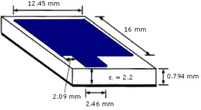
Figure 2 Geometry of the Microstrip Patch Antenna
Microstrip patch antenna is shown in figure.2; we are going to analyze the internal properties of the antenna. Mainly focus to find the scattering parameter of the antenna. S11 is depending on the geometry of the antenna, it is crucial that to model metallic patch dimensions as closely as possible. Cell size of the antenna is 0.05 mm to accurate get the dimensions. Then we could model the X direction as 12.45 mm, Y direction as 16 mm, and thickness of the substrate as 0.05 or 0.1 mm. This has two drawbacks, one is the accuracy of the thickness of the substrate would be unacceptable, and the dimensions of the rectangular patch in FDTD cells would be 249 by 320. Even though the Z direction would be small.
This is one of those times when it is better to use cells with different sizes in the different directions. Following the example of sheen, et al. [5], we choose Δx = 0.389 mm, Δy = 0.4 mm and Δz = 0.265 mm. Now we have a rectangular patch that is 32 Δx by 40 Δy, the substrate is 3 Δz thick. In choosing the time step, we take the smallest dimension Δz,
econds
pi
c
z
t
0
.
441
cos
2
0
(53)6812
.
0
389
.
0
265
.
0
x
z
x
(54)6625
.
0
400
.
0
265
.
0
x
z
y
(54)V. MATERIALS MODELLING
We will assume that we are only dealing with three materials: (1) free space (2) the dielectric material of the substrate and metal. We will assume that the substrate has a relative dielectric constant of 2.2. Therefore the relationship between the flux density and electric field need the following equation,
ex [i] [j] [k] = gax [i] [j] [k] * dx [i] [j] [k] (56) and gax [i] [j] [k] = 1/2.2 (57)
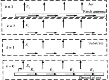
At those points corresponding to the substrate. Metal could be specified by ensuring that the E fields within those points corresponding to metal remain as zero. Setting gax, gay and gaz equal to zero. Fields are indicated in the following figure. 3
Figure 3 Positions of the fields
Figure 3 shows that the entire configuration lays on a ground plane, so we will specify all Ex and Ey values for k = 0 to remain at zero. However, since the Ez value at k = 0 lies 1/2 cell above the k = 0 plane, it will be in the substarte. Similarly, in specifying the metal of the antenna, Ex , Ey are set to zero for the k = 3 level, but Ez at k = 0 in free space.
Figure 4 Positions of the E field relative to the materials Being modeled
i
ja
k
ez
i
ja
k
shape
i
k
hx
inc
ja
ex
0
.
5
_
(58)
i
ja
k
hx
i
ja
k
shape
i
k
ez
inc
ja
hx
1
1
0
.
5
_
(59)The function shape [i] [k] has the value of one for that portion directly under the stripline and zero everywhere else. Boundary conditions we are using PML method, but that was always for homogenous medium. Half medium is the dielectric substrate, and half is free space, so PML is not suitable for this problem. We have to do some minor changes in the one dimensional equation.
j
eps sub
hx inc
j hx inc
j
gjj inc ez j gj j inc ez
_ 1 _ _
/ 5 . 0 2
_ 3 _
(60)
0
.
5
_
_
1
2
_
3
_
j
inc
ez
j
inc
ez
j
fj
j
inc
hx
j
fj
j
inc
hx
(61)
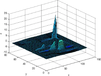
Figure 5 Current Distribution of the Microstrip Patch Antenna
Figure 6 Current distribution
VI. CALCULATING THE S11
To calculate V1, we need Ez at three points in k direction between the ground plane and the lead of the conductor. In
practice, any one of the Ez values is adequate because magnitude divides out. Fig.7 shows the time domain data from a simulation result for source voltage. The first 350 points are taken as the input and the rest of the data is the reflection coming out of the conductor.
Figure 7 Patch Antenna Source Voltage with Time steps
Source magnetic field versus time steps are plotted in figure 8. This also matching in the time steps of 4000. The source voltage and currents are Fourier transformed using an FFT with the same number of terms. The results for source voltage and current, for 4000 time steps were padded with zeroes to fill the FFT. Then the resulting complex
voltages and currents were divided at each frequency to determine the input impedance Zinat the feed location.
Figure 8 Microstrip Patch Antenna source current with time steps
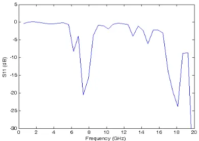
To calculate the return loss equation is given by,
f
E
f
E
f
S
in out
dB 10
11
20
log
(62)Return loss parameter is plotted in the figure. 9
VII. CONCLUSION
FDTD analysis for Microstrip Patch Antenna is presented. The versatility of the FDTD method allows easy calculation of many complicated Microstrip structures. With the computational power of computers increasing rapidly, this method is very promising for the computer-aided design of many types of Microstrip circuit components and this analysis is useful for wireless applications.
REFERENCES
[1] K. S. Yee, “Numerical solution of initial boundary value problems involving Maxwell’s equations in isotropic media,” IEEE Transactions on. Antennas and Propagation, vol. 14, pp. 302–307, May 1966.
[2] J. Schneider and S. Hudson, “The finite-difference time-domain method applied to anisotropic material,” IEEE Transaction Antennas Propagation, vol. 41, pp. 994–999, July 1993.
[3] R.J.Luebbers, Fellow, IEEE, and H. S. Langdon, “ASimple Feed Model that Reduces Time Steps Needed for FDTD Antenna and Microstrip Calculations,” IEEE Transaction on Antennas and Propagation, vol.44, no.1, July 1996.
[4] S. G. Garcia, T. M. Hung-Bao, R. G. Martin, and B. G. Olmedo, “On the application of finite methods in time domain to anisotropic dielectric waveguides,” IEEE Trans. Microwave Theory Tech., vol. 44, pp. 2195–2206, Dec. 1996.
[5] D.M. Sheen, S.M.Ali, Mohamad and Kong, “Application of the Three-Dimensional Finite- Difference Time-Domain Method to the Analysis of Planar Microstrip Circuits”, IEE Transaction on Microwave Theory and Techniques, vol.38, no.7, July 1990.
[6] C. L. Longmire, "State of the art in IEMP and SGEMP calculations," IEEE Trans. Nucl. Sci., vol. NS-22, pp. 2340-2344, Dec. 1975. [7] Wenhua Yu, Xaoling Yang, Yongjun Liu, Lai-Ching Mal, Tao Sul, Neng-Tien Huang,
[8] Raj Mittra, “A New Direction in Computational Electromagnetics: Solving Large Problems Using the Parallel FDTD on the BlueGeneIL Supercomputer Providing Teraflop-Level Performance”, IEEE Antennas and Propagation Magazine, vol.50, no.2, pp. 26 – 44, April2008.
[9] W. Yu, Raj Mittra, T. Su, Y. Liu, and X. Yang, Parallel Finite Difference Time Domain Method, Norwood, MA, Artech House, June 2006.
[10] Atef Elsherbeni and Veysel Demir, “The Finite Difference Time Domain Method for Electromagnetics”,ISBN13: 9781891121715, SciTech Publishing, 2009.
BIBLIOGRAPHY
T.Shanmuganantham received B.E. degree in Electronics and Communication Engineering
from University of Madras, M.E. degree in Communication Systems from Madurai Kamaraj University and Ph.D. (Gold Medal) in the area of Antennas from National Institute of Technology, Tiruchirappalli, India under the guidance of Dr.S.Raghavan. He has 12 years of
teaching experience in various reputed Engineering colleges such as SSN College of Engineering, National Institute of Technology and Science. Presently he is working as Assistant Professor in Department of Electronics Engineering, School of Engineering & Technology, Pondicherry University, Pondicherry. His research interest includes Microwave/Millimeter-Wave Circuits and Devices, Microwave Integrated Circuits, Antennas, EMI/EMC, Computational Electromagnetics, MEMS, Metamaterials. He has published 40 research papers in various national and International level Journals and Conferences. He is a member in IEEE, Life Member in IETE, Institution of Engineers, CSI, Society of EMC and ISTE.
Dr.S.Raghavan having 31 years of Teaching (U.G., P.G. and Research) experience in the
National Institute of technology, Tiruchirappalli, India as a Senior Professor. Developed Microwave and Microwave Integrated Circuits Lab. Obtained B.E.(Electronics and Communication Engineering) degree from College of Engineering , Guindy. M.Sc.(ENGG.)Microwave Engineering from College of Engineering, Trivandrum and Ph.D.(Microwave Integrated Circuits) from I.I.T., Delhi, India under the guidance of
Prof.Baharathi Bhat and Prof.S.K.Koul. Senior Member of IEEE in MTT and EMBS. Life