Design of Modified Carry Select Adder with
Low Power and Efficient Area Using D-Latch
B. Vijaya Lakshmi, B. Praveen Kumar
M. TECH Student, VLSI Design, Department of Electronics and Communication Engineering, Sri Aditya College
of Engineering and Technology, India
Assistant Professor, Department of Electronics and Communication Engineering, Sri Aditya College of Engineering
and Technology, India
ABSTRACT: Carry select adder (CSLA) is a one of the high speed adders used in many computational systems to perform fast arithmetic operations. Due to the rapidly growing mobile industry not only the faster arithmetic unit but also less area and low power arithmetic units are needed. The modified CSLA architecture has developed using Binary to Excess-1 converter (BEC).This paper proposes an efficient method which replaces the BEC using D latch .Experimental analysis shows that the proposed architecture achieves the three folded advantages in terms of area, delay and power.
KEYWORDS: Low Power, CSLA, Area Efficient , BEC, Multiplexer.
I.
INTRODUCTION
Design of area- and power - efficient high- speed data path logic systems are one of the most substantial areas of research in VLSI system design. In digital adders, the speed of addition is limited by the time required to propagate a carry through the adder. The sum for each bit position in an elementary adder is generated sequentially only after the previous bit position has been summed and a carry Propagated into the next position.
The CSLA is used in many computational systems to alleviate the problem of carry propagation delay by independently generating multiple carries and then select a carry to generate the sum. The carry Select adder (CSLA) provides a compromise between small areas but longer delay ripple carry adder (RCA) and larger area with shorter delay carry look-ahead adder. CSLA uses multiple pairs of ripple carry adder (RCA) to generate partial sum and carry by considering carry multiplexers. The modified CSLA using BEC has reduced area and power consumption with slight increase in delay. The basic idea of the proposed architecture is that which replaces the BEC by D latch with enable signal. The proposed architecture reduces the area, delay and power. This paper is organized as follows section III presents the detailed structure and the function of the binary to excess-1 convert logic. Section VI and Section V explains the regular and modified CSLA respectively. Deals with the proposed architecture. Results are analyzed in the section VII. Section VIII concludes.
II.LITERATUREREVIEW
III.BEC
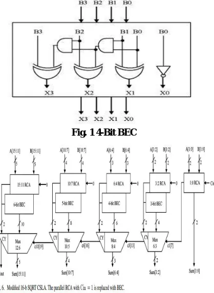
To reduce the area and power consumption of regular CSLA, RCA with Cin=1 is replaced with BEC. An n+1 bit BEC replaces the n bit RCA. The function table of a 4-bit BEC is shown in Fig. 1 and Table 1 respectively. By the use of BEC logic, we can reduce the significant amount of silicon area reduction in the VLSI design. The Boolean expression of the 3-bit BEC is given below. S0=~B0 , S1=B1^B2
S2=B2(B0&B1
Fig. 1 4-Bit BEC
Fig: 2 modified SQRT CSLA
IV.REGULARSQRTCSLA
V .MODIFIED CSLA USING BEC
The structure of the proposed 16-bit SQRT CSLA using BEC for RCA with Cin=1 to optimize the area and power is shown in Fig .4. We again spilt the structure into five groups. The delay and area estimation of each group 2 is shown in Fig.5. One input from the BEC. Comparing the group 2 of both regular and modified CSLA, it is clear that BEC structure reduces the area and power. But the disadvantage of BEC method is that the delay is increasing than the regular CSLA
.
Fig: 3 Existences CSLA
Fig: 5 Modified RTL diagram
VI. MODIFIED 16-BIT CSLA USING D-LATCH
If the actual carry input is one, then computed sum and carry latch is accessed and for carry input zero. MSB adder is accessed. Cout is the output carry. The Fig.9 shows the internal structure of group 2 of the proposed 16-bit CSLA. The group 2 performed the two bit addition which is a2 with b2 and a3 with b3
Fig7: Modified RTL diagram
This is done by two full adder (FA) named FA2 and FA3 respectively. The third input to the full adder FA2 is the clock instead of the carry and the third input to the full adder FA3 is the carry output from FA2. The group 2 structure has five D-Latches in which four are used for store the sum2 and sum3 from FA2 and FA3 respectively and the last one is used to store carry. Multiplexer is used for selecting the actual sum and carry according to the carry is coming from the previous stage. The 6:3 multiplexer is the combination of 2:1 multiplexer. When the clock is low a2 and b2 are added with carry is equal to zero. Because of low clock, the first D-Latch is not enabled. The second D-Latch store the sum with cin =0 by using inverted clock enable. When the clock is high, the addition is performed with carry is equal to one. The other D-Latches enabled and store the sum and carry for carry is equal to one. According to the value of c1 whether it is 0 or 1, the multiplexer selected the actual sum and carry.
VII .SIMULATION RESULTS
Fig.9 CSLA using BEC
e fig. We change the MOSFET’s configuration for the better results. Here we work on the current and voltage of the MOSFET’s.We
Fig.10 Modified CSLA using D-Latch
Adder(16-bit) Delay(ns) Power(mW) PDP(x10^-12) Regul
ar 20.7 1710.63 35410.04 SQRT
CSLA
CSLA using 21.598 874.37 18884.64 BEC
Modified 17.84 324.21 5783.906 CSLA using
In table we are discussing about the difference between the existences and modified that is delay, power.
VIII. CONCLUSION
A simple approach is proposed in this paper to reduce the area and power of SQRT CSLA architecture. The reduced number of gates of this work offers the great advantage in the reduction of area and also the total power (Table II).The modified CSLA reduces the area and power when compared to regular CSLA with increase in delay by the use of Binary to Excess-1 converter. This paper proposes a scheme which reduces the delay, area and power than regular and modified CSLA by the use of D-latches.
REFERENCES
[1] Sudheer Kumar Yezerla, B Rajendra Naik. “Design and Estimation of delay, power and area for Parallel prefix adders” Proceedings of 2014 RAECS UIET Panjab University Chandigarh, 06 - 08 March, 2014.
[2] N. H. E. Weste and D. Harris, CMOS VLSI Design, 4th edition,Pearson–Addison-Wesley, 2011.
[3] R. P. Brent and H. T. Kung, “A regular layout for parallel adders,” IEEE Trans. Comput., vol. C-31, pp. 260-264, 1982. [4] Y. Choi, "Parallel Prefix Adder Design", Proc. 17th IEEE Symposium on Computer Arithmetic, pp. 90-98, 27th June 2005.
[5] Basant Kumar Mohanty and Sujit Kumar Patel “Area–Delay–Power Efficient Carry-Select Adder,” IEEE transaction on circuits and systems-II: Express briefs, VOL. NO. 6, JUNE 2014.
[6] L. Mugilvannan and S. Ramasamy “Low-Power and Area-Efficient Carry Select Adder Using Modified BEC-1 Converter” IEEE-31661. 4th
ICCCNT2013 July 4-6, 2013, Tiruchengode, India.
[7] T. Lynch and E. E. Swartzlander, “A Spanning Tree Carry Look ahead Adder,” IEEE Trans. On Computers, vol. 41, no. 8, pp. 931-939, Aug.1992.
[8] D. Jaya Kumar, Dr.E. Logashanmugam, ―Performance Analysis of FIR filter using Booth Multiplier‖, IEEE July 2014.
[9] Shelja Jose, Shereena Mytheen ,‖Modified Booth Multiplier Based Low-Cost FIR Filter Design” International Journal of Engineering Science and
Innovative Technology (IJESIT) Volume 3, Issue 5, September 2014.
[10] Sarita Chouhan1,Yogesh Kumar2, ―Low power designing of FIR filters‖, ISSN No: 2250-3536 ,May 2012.
[11] Rashidi B, Pourormazd M ―Design and implementation of low power digital FIR filter based on low power multipliers and adders on xilinx FPGA‖,IEEE April 2011.
[12] Ravikumar A Javali, Ramanath J Nayak, Ashish M Mhetar, Manjunath C Lakkannavar‖ Design of High Speed Carry Save Adder using Carry
Lookahead Adder “Proceedings of International Conference on Circuits, Communication, Control and Computing (I4C 2014).
[13] O. J. Bedrij, ―Carry-select adder,‖ IRE Trans. Electron. Comput., pp. 340–344, 1962.
[14] B. Ramkumar, H.M. Kittur, and P. M. Kannan, ―ASIC implementation of modified faster carry save adder,‖ Eur. J. Sci. Res., vol. 42, no. 1, pp.
53–58, 2010.
[15] T. Y. Ceiang and M. J. Hsiao, ―Carry-select adder using ripple carry adder.. 2012
[16] Y. Kim and L.-S. Kim, ―64-bit carry-select adder with BEC . May 2014.
Ramkumar, B. and Harish M Kittur, (2015) ‗Low Power and Area Efficient Carry Select Adder‘, IEEE Transactions on Very Large Scale Integration