Design of Low Power Consumption and Area
Efficient Modified Carry Select Adder with
D-Latch on a Reconfigurable Hardware
C. Dharsana*, G.Dhivya*, D.Dhivya*, V.N.Veena
** UG Students, Department of Electronics and Communication Engineering, Maharaja Engineering College, Avinashi,
Tamilnadu, India
ABSTRACT: Design of area- and power-efficient high-speed data path logic systems are one of the most substantial areas of research in VLSI system design. In digital adders, the speed of addition is limited by the time required to propagate a carry through the adder. Carry SeLect Adder (CSLA) is one of the fastest adders used in many data-processing processors to perform fast arithmetic functions. From the structure of the CSLA, it is clear that there is scope for reducing the area and power consumption in the CSLA. This work uses a simple and efficient gate-level modification to significantly reduce the area and power of the CSLA. Based on this modification 8-bit, 16-bit, 32-bit, and 64-bit square-root CSLA architecture have been developed and compared with the regular SQRT CSLA architecture. The proposed design has reduced area and power as compared with the regular SQRT CSLA with only a slight increase in the delay. This work evaluates the performance of the proposed designs in terms of delay, area, power.
KEYWORDS: Application-specific integrated circuit (ASIC), area-efficient, CSLA, low power, SQRT CSLA.
I. INTRODUCTION
At present, many electronic systems require integrated dedicated components that are specialized to perform a task or a limited set of tasks. Some circuits in this may not be produced in large volume because of the specificity of their application. The size of the circuit, usually measured in terms of the number of active devices (e.g. transistors), requires handling of the design data with systematic techniques. In addition, optimizing features of large-scale circuits is an even more complex problem because the feasible implementation choices grow rapidly in number with the circuit size. Microelectronics has been the enabling technology for the development of hardware and software system in the recent decades. The continuously increasing level of integration of electronics devices on a single substrate has led to the fabrication of increasingly complex system. The integrated circuit technology, based on the use of semiconductor materials, has progressed tremendously. While a handful of devices were integrated on the first circuit in the 1960s, circuits with over one million devices have been successfully manufactured in the late 1980s. Such circuits often called Very Large Scale Integrated (VLSI).
Vol. 5, Issue 3, March 2017
II. CARRY SELECT ADDER
The carry select adder generally consists of two ripple carry adders and a multiplexer. Adding two n-bit numbers with a carry select adder is done with two adders (therefore two ripple carry adders) in order to perform the calculation twice, one time with the assumption of the carry being zero (Cin = 0) and the other assuming one (Cin = 1).
After the two results are calculated, the correct sum, as well as the correct carry, is then selected with the multiplexer once the correct carry is known. The blocks representation CSLA is shown in Fig.1. The basic building block of a carry select adder is shown in Fig.2, where the block size is 4. Two 4-bit ripple carry adders are multiplexed together, where the resulting carry and sum bits are selected by the carry-in. Since one ripple carry adder assumes a carry-in of 0, and the other assumes a carry-in of 1, selecting which adder had the correct assumption via the actual carry-in yields the desired result [3].
2.1.UNIFORM SIZED CSLA
A 16-bit carry select adder with a uniform block size of 4 can be created with three of these blocks and a 4-bit ripple carry adder [4]. Since carry-in is known at the beginning of computation, a carry select block is not needed for the first four bits. The delay of this adder will be four full adder delays, plus three mux delays, this shown in Fig.3.
Fig.1 Block Diagram of CSLA Fig.2Basic Building Blocks of CSLA
2.2.VARIABLE SIZED CSLA
A 16-bit carry select adder with variable size can be similarly created. Fig.4 shows an adder with block sizes of 2-2-3-4-5. This break-up is ideal when the full-adder delay is equal to the MUX delay, which is unlikely.
The total delay is two full adder delays, and four mux delays. In total, the carry propagation time through an n-bit adder block is reduced from O(n) to the number of stages times the delay of the multiplexers. Naturally, using n blocks of 1-bit carry-select adders would incur a complexity of n multiplexers, again resulting in O(n) delay. Therefore, a partition with (slowly) increasing block-size is chosen.
In the example, the first (least-significant) block consists of a simple full adder, followed by a 3-bit carry-select block, and finally a 4-bit carry-carry-select block. A common choice for a 16-bit carry-carry-select adder is to use a 6-4-3-2-1 bit partitioning. While the delay of the standard ripple-carry adder with n-bits is O(n), the delay through the carry-select adder behaves as O(sqrt(n)) at a hardware cost of O(3*n).
Fig.4 Variable Sized CSLA
2.3.DELAY AND AREA EVALATION OF XOR GATE
The basic idea of this work is to use Binary to Excess-1 Converter (BEC) instead of RCA with Cin = 1 in the
regular CSLA to achieve lower area and power consumption. The main advantage of this BEC logic comes from the lesser number of logic gates than the n-bit Full Adder (FA) structure [5].
Fig.5Delay and Area Evaluation of an XOR Gate.
Vol. 5, Issue 3, March 2017
III. BINARY TO EXCESS - 1 CONVERTER
The main idea of this work is to use BEC instead of the RCA with Cin = 1 in order to reduce the area and
power consumption of the regular CSLA. To replace the n-bit RCA, an n+1bit BEC is required. A structure and the function table of a 4-b BEC are shown in Fig.6 and Table.1, respectively.
Fig.6 4-Bit BEC
3.1.CSLA FORMED BY USING BEC
Fig.7 illustrates how the basic function of the CSLA is obtained by using the 4-bit BEC together with the mux [6].
Table.1Function Table of the 4-Bit BEC B (3:0) X (3:0)
0000 0001
0001 0010
0010 0011
0011 0100
0100 0101
0101 0110
0110 0111
0111 1000
1000 1001
1001 1010
1010 1011
1011 1100
1100 1101
1101 1110
1110 1111
1111 0000
One input of the 8:4 mux gets as it input (B3, B2, B1, and B0) and another input of the mux is the BEC output. This produces the two possible partial results in parallel and the mux is used to select either the BEC output or the direct inputs according to the control signal Cin. The importance of the BEC logic stems from the large silicon area reduction when the CSLA with large number of bits are designed. The Boolean expressions of the 4-bit BEC is listed as (The functional symbols ~ (NOT), & (AND), ^(XOR)).
IV. 16 - BIT SQUARE - ROOT CSLA
The 16-bit conventional CSLA is shown in Fig.8. It has 17-half adders and 15-full adders. Since the ripple carry adder (RCA) is used in the final stage, this structure yields large carry propagation delay. The simplified square root CSLA is shown in the Fig.9.To reduce this delay, the final stage of CSA is divided into 5 groups as shown in Fig.10. The first group includes1+ log2 n-bit value and other groups includes n2 log -bit value, where nis the bit size of the adder. The divided groups are listed below,
{c4,s[4:0]}
{c7,x[7:5]}
{c10,x[10:8]}
{c13,x[13:11]}
x[17:14]
Fig.74-Bit BEC with 8:4 mux
The first group of output s[4:0] are directly assigned as the final output; the second group {c7,x[7:5]} manipulates the partial result by considering c4 is 0; the third group {c10,x[10:8]} manipulates the partial result by considering c7 is 0; the fourth group {c13,x[13:11]} manipulates the partial result by considering c10 is 0 and the fifth group x[17:14] manipulates the partial result by considering c13 is 0.
Fig.816-Bit CSLA
Vol. 5, Issue 3, March 2017
final result without the carry propagation delay from c10 to c13 and depending on c13 of the fourth group final result, the fifth group mux gives the final result without the carry propagation delay from c13 to s17
Fig.9Simplified 16-Bit CSLA
The main advantage of this logic is that each group computes the partial results in parallel and the muxes are ready to give the final result “immediately” with the minimum delay of the mux. When the Cinof each group arrives, the final
result will be determined “immediately”. Thus the maximum delay is reduced in the carry propagation path. This same logic has been used for 32 and 64-bit adder structures to achieve higher speeds.
Fig.10 CSLA Output with Five Groups
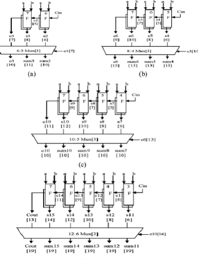
4.1.DELAY AND AREA EVALUATION
The delay and area evaluation of each group are shown in Fig.11, in which the numerals within [] specify the delay values, e.g., sum2 requires 10 gate delays. The steps leading to the evaluation are as follows.
The group2 [see Fig. 5.4(a)] has two sets of 2-b RCA. The arrival time of selection input C1 [time (t) = 7] of 6:3
mux is earlier than S3 [t = 8] and later than S2 [t = 6]. Thus, Sum3 [t = 11] is summation of S3 and mux [t=3] Sum2 [t=10] is summation of C1 and mux.
Except for group2, the arrival time of mux selection input is always greater than the arrival time of data outputs from the RCA’s. Thus, the delay of group3 to group5 is determined, respectively as follows:
{c6, sum [6:4]} = c3 [t=10] + mux {c10, sum [10:7]} = c6 [t=13] + mux {Cout, sum [15:11]} = c10 [t=16] + mux
V. MODIFIED 16 BIT SQUART – ROOT CSLA
The structure of the proposed 16-b SQRT CSLA using BEC for RCA with Cin = 1 to optimize the area and
power is shown in Fig.12. Then again split the structure into five groups. The delay and area estimation of each group are shown in Fig.13. The steps leading to the evaluation are given here,
The group2 [see Fig. 13(a)] has one 2-b RCA which has 1 FA and 1 HA foR Cin = 0. Instead of another 2- bit RCA with Cin = 1 a 3-b BEC is used which adds one to the output from 2-b RCA. Based on the consideration of delay values of Table II, the arrival time of selection input C1[time(t) = 7] of 6:3 mux is earlier than s3[t = 9] and c3= [t = 10] and later than the s3[t = 4]. Thus, the sum3 and final c3 (output from mux) are depending on s3 and mux and partial c3 (input to mux) and mux, respectively. The sum2 depends on c1 and multiplexer.
Fig.11Delay and Area Evaluation of Regular SQRT CSLA: (a) Group2, (b) Group3, (c) Group4, and (d) Group5. F is a Full Adder
Vol. 5, Issue 3, March 2017
Fig.13Delay and Area Evaluation of Modified SQRT CSLA: (a) Group2, (b) Group3, (c) Group4, and (d) Group5. H is a Half Adder
For the remaining group’s the arrival time of mux selection input is always greater than the arrival time of data inputs from the BEC’s. Thus, the delay of the remaining groups depends on the arrival time of mux selection input and the mux delay. The area count of group2 is determined as follows;
Gate count = 43 (FA + HA + Mux + BEC) FA = 13(1 * 13)
HA = 6(1 * 6) AND = 1 NOT = 1 XOR = 10(2 * 5)
VI. SIMULATION RESULTS
The main module of the simulation of regular and modified carry select adder in 8-bit and 16-bit are given as follows,
6.1. Regular CSA in 8 – Bit Operation
The main module of regular CSA in 8- bit operation is regular_csa8. The simulation result of regular CSA in 8- bit operation is shown in Fig.14. This regular CSA in 8- bit operation is simulated in ModelSim using VHDL coding. Here “a” and “b” are the 8 – bit input vectors and “s_out” is 8 – bit output vector.
6.2. Modified CSA in 8- Bit Operation
The main module of modified CSA in 8- bit operation is mod_csa8. The simulation result of modified CSA in 8- bit operation is shown in Fig.15. This modified CSA in 8- bit operation is simulated in ModelSim using VHDL coding. Here “a” and “b” are the 8 – bit input vectors and “s_out” is 8 – bit output vector.
6.3. Regular CSA in 16 – Bit Operation
The main module of regular CSA in 16- bit operation is regular_csa_16. The simulation result of regular CSA in 16- bit operation is shown in Fig.16. This regular CSA in 16- bit operation is simulated in ModelSim using VHDL coding. Here “a” and “b” are the 16 – bit input vectors and “s_out” is 16 – bit output vector.
6.4. Modified CSA in 16- Bit Operation
The main module of modified CSA in 16- bit operation is mod_csa_16. The simulation result of modified CSA in 16- bit operation is shown in Fig.17. This modified CSA in 16- bit operation is simulated in ModelSim using VHDL coding. Here “a” and “b” are the 16 – bit input vectors and “s_out” is 16 – bit output vector.
Fig.16Regular CSA in 16- Bit Operation Fig.17Modified CSA in 16- Bit Operation
6.5. Power Result for Regular CSA in 8 - Bit Operation
The main module of regular CSA in 8 - bit operation is regular_csa8. The power result of regular CSA in 8 - bit operation is shown in Fig.18. This power report of regular CSA in 8 - bit operation is synthesized using Xilinx.
Vol. 5, Issue 3, March 2017
6.6. Power Result for Modified CSA in 8 - Bit Operation
The main module of modified CSA in 8 - bit operation is mod_csa8. The power result of modified CSA in 8 - bit operation is shown in Fig.19. This power report of modified CSA in 8 - bit operation is synthesized using Xilinx.
6.7. Power Result for Regular CSA in 16 - Bit Operation
The main module of regular CSA in 16 - bit operation is regular_csa_16. The power result of regular CSA in 16 - bit operation is shown in Fig.20. This power report of regular CSA in 16 - bit operation is synthesized using Xilinx.
Fig.20Regular CSA in 16 - Bit Operation Fig.21Modified CSA in 16 - Bit Operation
6.8. Power Result for Modified CSA in 16 - Bit Operation
The main module of modified CSA in 16 - bit operation is mod_csa_16. The power result of modified CSA in 16 - bit operation is shown in Fig.21. This power report of modified CSA in 16 - bit operation is synthesized using Xilinx.
VII.CONCLUSION
A simple approach is proposed in this paper to reduce the area and power of SQRT CSLA architecture. The reduced number of gates of this work offers the great advantage in the reduction of area and also the total power. The compared results show that the modified SQRT CSLA has a slightly larger delay (only 3.76%), but power of the 64-b modified SQRT CSLA are significantly reduced by 15.4%. The power-delay product and also the area-delay product of the proposed design show a decrease for 16-, 32-, and 64-b sizes which indicates the success of the method and not a mere tradeoff of delay for power and area. The modified CSLA architecture is therefore, low area, low power, simple and efficient for VLSI hardware implementation. It would be interesting to test the design of the modified 128-b SQRT CSLA. In future, the design can be further extend for higher number of bits.
REFERENCES
1. B. Ramkumar and Harish M Kittur, Low-Power and Area-Efficient Carry Select Adder, vol. 33 pp. 205-210 2. Bedrij.O.J,(1962), “Carry-select adder,” IRE Trans. Electron. Comput., pp. 340–344.
3. Ceiang .T.Yand Hsiao.M.J,(1998) “Carry-select adder using single ripple carry adder,” Electron. Lett., vol. 34, no. 22, pp. 2101–2103.
4. He.Y, Chang.C.H, and Gu.J,(2005) “An area efficient 64-bit square root carry-select adder for lowpower applications,” in Proc. IEEE Int. Symp. Circuits Syst., vol. 4, pp. 4082–4085.
5. Kim .Yand Kim.L.T,(2001) “64-bit carry-select adder with reduced area,” Electron. Lett., vol. 37, no. 10, pp. 614–615.