Xinlin Xia1, *, Yu Liu1, Hao Peng1, Minghuan Ni2, Haodong Lin1, and Yang Tao1
Abstract—In this letter, a compact ultra-wideband (UWB) bandpass filter based on CPW-to-microstrip transition structure is proposed. Compared with traditional UWB BPF using hybrid structures, the proposed filter has a more sharp selectivity due to a transmission zero located at the lower edge of the passband generated by the combined effect of both CPW-MS-CPW and interdigital coupling line (ICL). Moreover, to further improve its selectivity, the CPW open stubs (CPWOS) are introduced to produce two extra transmission zeros at high frequency. The measured results show that the proposed filter has some good characteristics such as sharp roll-off, compact size (0.54λg×0.38λg) and a very wide fractional bandwidth of 130%, which is a significant improvement to what has been reported for UWB BPF with similar structures.
1. INTRODUCTION
UWB bandpass filter (BPF) has received much interest since the US Federal Communication Commission (FCC) authorized the ultra-wideband (UWB) spectrum (3.1 to 10.6 GHz) for commercial use in 2002 [1]. As a result, several ideas and structures have been reported to implement UWB BPF [2–13]. In [2], a modified U-shaped MMR which has five resonance frequencies was used to improve the selectivity at upper edge of the passband. Similarly, in order to improve the selectivity, a novel MMR including open-circuited stubs and coupled-line sections was adopted in [3]. At the same time, several other UWB bandpass filters have been reported based on the transversal signal-interaction concepts [4, 5]. In these filters, input signal flows through two different signal paths so as to produce extra transmission zeros at the passband edges. Some transition structures have also been used to design ultra-wideband bandpass filter such as CPW-to-microstrip (MS) transitions [6–8] and MS-to-CPW transitions [9, 10]. In addition, some novel structures such as defected microstrip (DMS) structures [11, 12] and defected ground structures (DGS) [13] have been proposed in the last few years. Nevertheless, the use of DMS and DGS etched in the microstrip and ground plane, respectively, might destroy the signal integrity issues for packaging.
In this letter, a novel UWB bandpass filter using CPW — MS-CPW structure with good in-band and out-of-band performances is presented as shown in Fig. 1. The interdigital coupling line (ICL) and CPW open stubs (CPWOS) are applied to introduce extra three transmission zeros. As a result, compared with some traditional UBW bandpass filters using hybrid structures, the proposed filter has a sharper selectivity. In order to validate the performance of the proposed UWB bandpass filter, a filter prototype is designed, fabricated and measured. And the measured results are in close agreement with the simulated ones.
Received 30 December 2016, Accepted 3 February 2017, Scheduled 13 February 2017
* Corresponding author: Xinlin Xia ([email protected]).
Figure 1. Configuration of the proposed UWB BPF.
2. FILTER ANALYSIS AND DESIGN
The basic structure of the proposed CPW to MS transition structure and its equivalent J-inverter network are shown in Fig. 2(a) and Fig. 2(b), respectively. As mentioned in [7], the J-inverters are realized by the surface-to-surface coupling structure of CPW-to-MS transition structure. The middle microstrip of the proposed CPW-MS-CPW is replaced by an interdigital coupling line (ICL), which is different from the traditional hybrid CPW and MS structure presented in [7, 8]. As a result, two more transmission zeros could be obtained at the lower and higher stopband, respectively. As the simulated results shown in Fig. 3(b), its selectivity has been improved remarkably by using the ICL.
(a) (b)
Figure 2. (a) Layout of the proposed CPW-MS-CPW, (b) equivalent J-inverter network.
(a) (b)
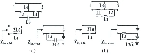
Figure 4. Equivalent low frequency lumped model, (a) the proposed CPW-MS-CPW with ICL, (b) traditional CPW-MS-CPW.
The transmission zero located at lower stopband could be explained by its low frequency lumped model shown in Fig. 4.
As for the CPW-MS-CPW with ICL presented in this paper, its equivalent low frequency lumped model and its even and odd-mode circuit are shown in Fig. 4(a). And its odd-mode input impedance (Zin,odd) and even-mode input impedance (Zin,enen) are shown in Eqs. (1)–(2).
Zin,odd = jω(2L0+L1) (1)
Zin,even =
jωL1 1−2ω2L
1C0
(2)
The condition of generating a transmission zero Zin,odd = Zin,even could be expressed by Eq. (3). And its solution is shown in Eq. (4).
ω2 = L0
L1C0(2L0+L1)
(3)
fz1 =
L0
L1C0(2L0+L1)
2π (4)
However, as for the traditional CPW-MS-CPW presented in [7], its equivalent low frequency lumped model and its even and odd-mode circuit are shown in Fig. 4(b). Its odd-mode input impedance (Zin,odd) and even-mode input impedance (Zin,even) are shown in Eqs. (5)–(6).
Zin,odd = jω(2L0+L1) (5)
Zin,even =
jωL1L2 2L1+L2
(6)
The condition of generating a transmission zeroZin,odd=Zin,even could be expressed by Eq. (7).
L1L2 2L1+L2
= (2L0+L1) (7)
Clearly, there is no transmission zero in low frequency except 0 GHz which is in accord with the simulation results shown in Fig. 3(b).
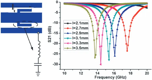
Figure 5. Configuration and simulatedS21 of the CPWOS.
(a) (b)
Figure 6. (a) Dimensions of the proposed filter, (b) photograph of the fabricated UWB BPF.
3. EXPERIMENTAL RESULTS
The final dimensions of the fabricated UWB BPF optimized by Ansoft HFSS 13 are (see Fig. 6(a)):
w0 = 0.24 mm, s0 = 3.5 mm, ws0 = 0.6 mm,ls0 = 22 mm, ls1 = 1.8 mm, ws3 = 0.1 mm, ls3 = 2.2 mm,
ls4 = 2.34 mm, r0 = 0.25 mm, r1 = 0.8 mm, l3 = 1 mm, w3 = 0.31 mm, d= 1.35 mm, ws1 = 0.45 mm,
ws4 = 0.7 mm, s3 = 0.1 mm, g = 0.15 mm, w1 = 0.2 mm, w2 = 0.1 mm, l1 = 6 mm. To verify our design, the fabricated UWB BPF was measured by an Agilent vector network analyzer E8363B. Fig. 7 shows the measured and simulated S parameters of the proposed UWB bandpass filter. Clearly, a good agreement between the experiment and simulation results is found. The tiny frequency shift is mainly caused by the fabrication and assembly errors. The measured results show that the proposed filter achieves a 3-dB fractional bandwidth of 130% (2.45–115 GHz). And the return loss is better than 125 dB from 3 to 111 GHz. Moreover, this filter exhibits sharp skirt characteristics. The lower skirt selectivity is 40 dB/GHz, and the selectivity factor (BW|3 dB/BW|30 dB) is 0.81. The group delay is under 0.25 ns in the frequency range of 1 to 18 GHz. The variation is less than 0.1 ns over the whole UWB passband.
(a) (b)
Figure 7. Simulated and measured results of the fabricated UWB BPF, (a)S parameters, (b) group delay.
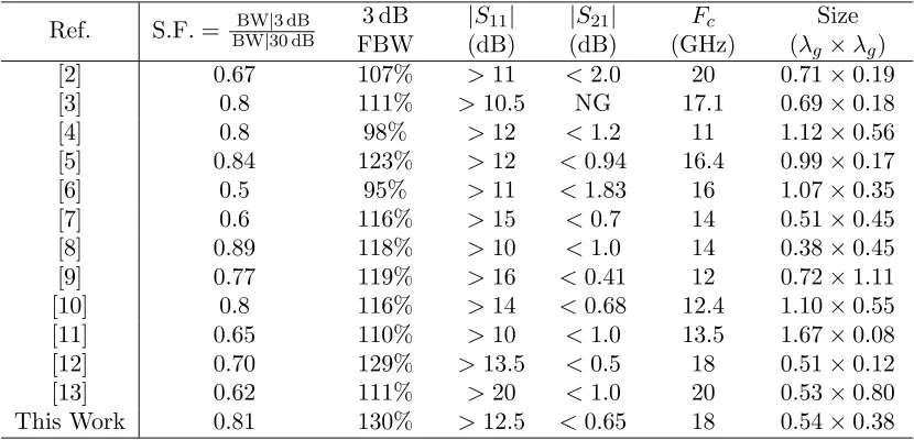
Table 1. Performance comparison between the proposed filter and others.
Ref. S.F. = BWBW||30 dB3 dB 3 dB FBW
|S11| (dB)
|S21| (dB)
Fc
(GHz)
Size (λg×λg) [2] 0.67 107% >11 <2.0 20 0.71×0.19 [3] 0.8 111% >10.5 NG 17.1 0.69×0.18 [4] 0.8 98% >12 <1.2 11 1.12×0.56 [5] 0.84 123% >12 <0.94 16.4 0.99×0.17 [6] 0.5 95% >11 <1.83 16 1.07×0.35 [7] 0.6 116% >15 <0.7 14 0.51×0.45 [8] 0.89 118% >10 <1.0 14 0.38×0.45 [9] 0.77 119% >16 <0.41 12 0.72×1.11 [10] 0.8 116% >14 <0.68 12.4 1.10×0.55 [11] 0.65 110% >10 <1.0 13.5 1.67×0.08 [12] 0.70 129% >13.5 <0.5 18 0.51×0.12 [13] 0.62 111% >20 <1.0 20 0.53×0.80 This Work 0.81 130% >12.5 <0.65 18 0.54×0.38
S.F.: selectivity factor of the passband; Δf|3 dB, Δf|30 dB: 3 dB bandwidth and 30 dB bandwidth of the passband;Fc: the upper-stopband frequency with 20 dB attenuation level; λg: the guided
wavelength at 6.85 GHz NG: Not Given.
achieved. Even though the filter presented in [8] has sharp roll-off,FC (upper stopband frequency with 20-dB attenuation) is less than 14 GHz. In this work, the Fc of the proposed UWB BPF is expanded to 18 GHz.
4. CONCLUSIONS
In this letter, a novel ultra-wideband bandpass filter is proposed and analyzed. Moreover, its selectivity is significantly improved by introducing an interdigital coupling line (ICL) and CPW open stubs (CPWOS). Finally, to verify the design, a prototype of the proposed filter is fabricated and measured in the frequency band of 1–18 GHz. This UWB BPF shows good performance on both in-band and out-of-band such as sharp selectivity, low insertion loss (<0.65 dB), and compact size (0.54λg×0.38λg),
1. Federal Communications Commission, “Revision of Part 15 of the commission’s rules regarding ultra-wideband transmission systems,” First Report and Order, FCC 02, V48, Apr. 2002.
2. Jhariya, D., A. R. Azad, A. Mohan, and M. Sinha, “A compact modified U-shaped UWB bandpass filter,” Microw. Opt. Technol. Lett., Vol. 57, No. 9, 2172–2175, Sep. 2015.
3. Zhang, T., F. Xiao, J. Bao, and X. Tang, “Compact ultra-wideband bandpass filter with good selectivity,” Electron. Lett., Vol. 52, No. 3, 210–212, Feb.–Nov. 2016.
4. Feng, W. J., W. Q. Che, and T.-F. Eibert, “Ultra-wideband bandpass filter based on transversal signal-interaction concepts,” Electron. Lett., Vol. 47, No. 24, 1330–1331, Nov. 2011.
5. Mirzaee, M. and B. S. Virdee, “UWB bandpass filter with notch-band based on transversal signal-interaction concepts,”Electron. Lett., Vol. 49, No. 6, 399–401, Mar. 2013.
6. Hu, H. L., X. D. Huang, and C. H. Cheng, “Ultra-wideband bandpass filter using CPW-to-microstrip coupling structure,” Electron. Lett., Vol. 42, No. 10, 586–587, Mar. 2006.
7. Wang, K., S. M. Wong, and Q.-X. Chu, “A compact UWB CPW bandpass filter with short-ended H-shaped resonator and controllable notched band,”Microwave. Opt. Technol. Lett., Vol. 55, No. 7, 1577–1581, 2013.
8. Lin, H., X. Xia, Z. Guo, and T. Yang, “Compact UWB filter with high selectivity and a deep notched band,”Progress In Electromagnetics Research Letters, Vol. 63, 123–128, 2016.
9. Ghazali, A. N., M. Sazid, and S. Pal, “A miniaturized microstrip-to-CPW transition based UWB-BPF with shaped roll-off and minimum insertion loss,”Microw. Opt. Technol. Lett., Vol. 58, No. 2, 289–293, Feb. 2016.
10. Ghazali, A. N., M. Sazid, and S. Pal, “Compact broadband balun-based UWB-BPF with minimum insertion loss and sharp selectivity,” Electron. Lett., Vol. 51, No. 15, 1174–1175, Jul. 2015.
11. Fallahzadeh, S. and M. Tayarani, “A new microstrip UWB bandpass filter using defected microstrip structures,”Journal of Electromagnetic Waves and Applications, Vol. 24, No. 7, 893–902, 2010. 12. Lin, H., H. Peng, X. Xia, T. Yang, and H. Jin, “A novel ultra-wideband bandpass filter using
defected microstrip structures,” IEICE Electron. Expr., Vol. 13, No. 7, 1–6, Apr. 2016.